DOI:
10.1039/C0NR00001A
(Paper)
Nanoscale, 2010,
2, 1171-1177
Change in conformation of polymer PFO on addition of multiwall carbon nanotubes
Received
2nd January 2010
, Accepted 3rd March 2010
First published on
21st May 2010
Abstract
Multiwall carbon nanotubes (MWNTs) have been added to the polymer poly (9,9-dioctylfluorenyl-2, 7-diyl) end capped with dimethylphenyl (PFO) in various weight percentages and the blends thus prepared, using a solution processing approach, have been characterized using SEM, UV-VIS spectroscopy, PL spectroscopy and I–V characterization. The SEM micrographs show a change in the structure of the polymer from partially crystalline to a glassy state in the blend form. The morphology observations are supported by absorption spectra which show a very high diminution of the polymers' beta peak in the spectra obtained from the polymer–nanotube blend. Thus, multiwall carbon nanotubes modify the local nanoscopic structure of PFO leading to a more glassy structure instead of a partially crystalline form and provide a method to tailor the conformation of polymer PFO, depending on intended application. I–V characteristics reveal an increase in current on formation of the polymer–nanotube blend as compared to the polymer-only structure. On the basis of percolation theory, as applied to these polymer–nanotube blends, a percolation threshold value of 0.45 wt% and critical exponent value of 1.84 has been obtained, indicating the formation of a three dimensional polymer–nanotube network.
1. Introduction
Composites/blends of conducting polymers with carbon nanotubes1–3 have caught the increasing attention of the scientific community in the last few years because of their potential applications in polymer light emitting diodes,4,5 photovoltaic cells and photodiodes,6 field effect transistors,7 optical limiting devices,8 supercapacitors,9 sensors,10etc. Among polyphenylene-based materials, highly emissive poly(9,9-dioctylfluorenyl-2, 7-diyl) end capped with dimethylphenyl (PFO) is a promising class of conjugated polymer, which can be used as blue light emitting material in polymer light emitting diodes.11 Pure blue light emission, remarkable thermal stability and high photo- and electroluminescence efficiency are some of the attractive properties of this polymer.12 We have added pristine multiwall carbon nanotubes (MWNTs) (synthesized using CVD approach) to the polymer PFO in various weight percentages and thus prepared PFO–MWNT blends, using a solution processing approach. The use of MWNTs is particularly important here, considering the fact that owing to their larger diameter and more complex multi-layered structure, MWNTs are essentially metallic in nature having a small but finite density of states at the Fermi level, much like graphite.13 Hence, separation of MWNTs into semiconducting and metallic types before utilization in an electronic application (for e.g. Organic Light Emitting Diodes (OLEDs), Organic Photovoltaics (OPVs), Organic Thin Film Transistors (OTFTs), etc.) is not required. The presence of two types of tubes in the case of single wall carbon nanotubes (SWNTs) is a big problem and separation of the two types of tubes in a 100% efficient manner is still an unsolved puzzle for the scientific community. The solution processed blends have been characterized using SEM, UV-VIS spectroscopy, PL spectroscopy and I–V characterization. The SEM micrographs show a change in the structure of the polymer from partially crystalline to a glassy state in the blend form. The morphology observations are supported by absorption spectra which show a very high diminution of the polymers' beta peak in the spectra obtained from the polymer–nanotube blend. Thus, multiwall carbon nanotubes modify the local nanoscopic structure of PFO leading to a more glassy structure instead of partially crystalline form and provide a method to tailor the conformation of polymer PFO, depending on the intended application. I–V characteristics reveal an increase in current on formation of polymer–nanotube blend as compared to the polymer-only structure. On the basis of percolation theory, as applied to these polymer–nanotube blends, a percolation threshold value of 0.45 wt% and critical exponent value of 1.84 has been obtained, indicating the formation of a three dimensional polymer–nanotube network.
2. Experimental details
The MWNTs were prepared using the CVD technique.14 A solution of ferrocene in toluene (in an appropriate ratio) was injected into a two stage furnace whose reaction zone was maintained at 750 °C. Argon was used as the carrier gas and its flow rate was adjusted in such a manner that the maximum quantity of precursor was consumed in the reaction zone. The first stage of the furnace was maintained at around 200 °C to ensure that the solution was vaporized as soon as it was injected (the vaporization temperature of ferrocene and toluene are 175 °C and 110 °C, respectively). MWNTs were found to grow predominantly in the centre of the reaction tube, which were then scraped out, after cooling the reaction tube to room temperature. The as prepared MWNTs were added to PFO polymer in toluene solution, in various weight percentages (0%, 0.25%, 0.5%, 2.0% and 5.0%) and sonicated for 2 h. PFO was obtained from the American Dye Source, Inc. (Product Code ADS129BE). ADS129BE is poly(9,9-dioctylfluorenyl-2,7-diyl) end capped with dimethylphenyl.15 Poly(3,4-ethylenedioxythiophene)![[thin space (1/6-em)]](https://www.rsc.org/images/entities/char_2009.gif) :
:![[thin space (1/6-em)]](https://www.rsc.org/images/entities/char_2009.gif) poly(styrenesulfonic acid) (PEDOT
poly(styrenesulfonic acid) (PEDOT![[thin space (1/6-em)]](https://www.rsc.org/images/entities/char_2009.gif) :
:![[thin space (1/6-em)]](https://www.rsc.org/images/entities/char_2009.gif) PSS) was obtained from Sigma Aldrich (Product No. 483095–250G). PEDOT
PSS) was obtained from Sigma Aldrich (Product No. 483095–250G). PEDOT![[thin space (1/6-em)]](https://www.rsc.org/images/entities/char_2009.gif) :
:![[thin space (1/6-em)]](https://www.rsc.org/images/entities/char_2009.gif) PSS was filtered using a Durapore PVDF membrane filter with a pore size of 0.45 μm. ITO coated glass substrates (25 mm × 25 mm, Rs = 20 Ω/□) having ITO thickness of 120 nm, were procured from Vin Karola, USA. These were patterned and then cleaned sequentially using a non-ionic detergent solution, distilled water, acetone, trichloroethylene and propanol respectively. After baking in vacuum oven for 30 min at 120 °C, a PEDOT
PSS was filtered using a Durapore PVDF membrane filter with a pore size of 0.45 μm. ITO coated glass substrates (25 mm × 25 mm, Rs = 20 Ω/□) having ITO thickness of 120 nm, were procured from Vin Karola, USA. These were patterned and then cleaned sequentially using a non-ionic detergent solution, distilled water, acetone, trichloroethylene and propanol respectively. After baking in vacuum oven for 30 min at 120 °C, a PEDOT![[thin space (1/6-em)]](https://www.rsc.org/images/entities/char_2009.gif) :
:![[thin space (1/6-em)]](https://www.rsc.org/images/entities/char_2009.gif) PSS layer was applied to these substrates, using a spin coating unit (SCU 2007 A Apex Instruments Co.), at 2000 rpm for 2 min. The thickness of the PEDOT
PSS layer was applied to these substrates, using a spin coating unit (SCU 2007 A Apex Instruments Co.), at 2000 rpm for 2 min. The thickness of the PEDOT![[thin space (1/6-em)]](https://www.rsc.org/images/entities/char_2009.gif) :
:![[thin space (1/6-em)]](https://www.rsc.org/images/entities/char_2009.gif) PSS layer was 100 ± 5 nm, as measured using an ellipsometer (J. A. Wollam Co. M-2000U). The PEDOT
PSS layer was 100 ± 5 nm, as measured using an ellipsometer (J. A. Wollam Co. M-2000U). The PEDOT![[thin space (1/6-em)]](https://www.rsc.org/images/entities/char_2009.gif) :
:![[thin space (1/6-em)]](https://www.rsc.org/images/entities/char_2009.gif) PSS layer was applied as a buffer layer. It improves the quality of the ITO electrode by minimizing the surface roughness of ITO and reducing the resistance between polymer layer and ITO. The PEDOT
PSS layer was applied as a buffer layer. It improves the quality of the ITO electrode by minimizing the surface roughness of ITO and reducing the resistance between polymer layer and ITO. The PEDOT![[thin space (1/6-em)]](https://www.rsc.org/images/entities/char_2009.gif) :
:![[thin space (1/6-em)]](https://www.rsc.org/images/entities/char_2009.gif) PSS coated substrates were baked in a vacuum oven at 120 °C for 2 h. After that, the substrates were cooled down to room temperature and PFO–MWNT solution blends with varying weight percentages of MWNTs (0%, 0.25%, 0.5%, 2.0% and 5.0%) were applied to different substrates using a spin coating unit, at 2000 rpm for 2 min. The thickness of the PFO–MWNT blend layer was 200 ± 10 nm, as measured using an ellipsometer. The solution blend coated substrates were baked in vacuum oven at 150 °C for 2 h and then allowed to cool down to room temperature. Subsequently, aluminium electrodes were deposited by vacuum evaporation technique. A schematic diagram which illustrates the structure is shown in Fig. 1.
PSS coated substrates were baked in a vacuum oven at 120 °C for 2 h. After that, the substrates were cooled down to room temperature and PFO–MWNT solution blends with varying weight percentages of MWNTs (0%, 0.25%, 0.5%, 2.0% and 5.0%) were applied to different substrates using a spin coating unit, at 2000 rpm for 2 min. The thickness of the PFO–MWNT blend layer was 200 ± 10 nm, as measured using an ellipsometer. The solution blend coated substrates were baked in vacuum oven at 150 °C for 2 h and then allowed to cool down to room temperature. Subsequently, aluminium electrodes were deposited by vacuum evaporation technique. A schematic diagram which illustrates the structure is shown in Fig. 1.
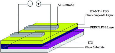 |
| | Fig. 1 Schematic sandwich geometry employed. | |
The as synthesized multiwall carbon nanotubes were examined using a scanning electron microscope (Carl Zeiss EVO® MA 10). The spin coated PFO–MWNT blend layer on ITO substrates was also examined using the same scanning electron microscope. HRTEM studies were carried out using Tecnai G2F-30 STWIN 300kV FEG HRTEM. Raman spectra were recorded using an Ar ion laser with an excitation wavelength of 514.5 nm and analyzed using a Renishaw Raman spectrometer (Invia reflex) equipped with a charge-coupled device in back scattering geometry. The optical absorption spectra of the PFO–MWNT blends were recorded using Perkin Elmer Lambda 25 UV/VIS Spectrophotometer. PL was measured using a home assembled system consisting of a two stage monochromator, a photomultiplier tube (PMT) with a lock-in amplifier for PL detection and an Ar+ ion laser operating at 405 nm and 5 mW (corresponding to 0.125 W cm−2) for excitation in all the measurements. The thickness of the films was measured using an ellipsometer. I–V measurements were carried out using a Keithley 2400 programmable voltage–current digital source meter.
3. Results and discussion
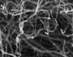
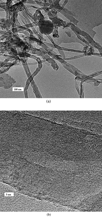
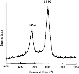
The SEM micrograph of synthesized multiwall carbon nanotubes (Fig. 2) shows the presence of multiwall carbon nanotubes with lengths in the range of hundreds of nanometres and diameters in the range of tens of nanometres (30–50 nm). The HRTEM micrograph (Fig. 3) confirms the multiwall structure of the nanotubes and shows an inner diameter of less than 10 nm and outer diameter in the range of tens of nanometres (30–50 nm). The Raman spectra (Fig. 4) shows the presence of a sharp peak at 1580 cm−1 (G band), corresponding to the high frequency E2g first order mode, and a peak at 1352 cm−1 (D band) corresponding to the disorder-induced mode. Thus, Raman spectra also confirm the formation of multiwall carbon nanotubes. Fig. 5 shows the structure of polymer PFO. Fig. 6 is a digital photograph of the PFO–MWNT solution blends with varying weight percentage of MWNTs (0%, 0.5%, 2.0% and 5.0%). It can be seen that the 0% solution is a clear yellowish solution of the pristine polymer whereas as the weight percentage of MWNTs in the solution increases, the solution changes colour from yellow to black. These solution blends were found to be stable over a period of more than 4 months i.e., the MWNTs were suspended indefinitely in the solution and did not precipitate out from the solution. Thus, modification of MWNTs with PFO units endows MWNTs with slightly better solubility and dispersibility in toluene.
 |
| | Fig. 5 Structure of polymer PFO (poly(9,9-dioctylfluorenyl-2,7-diyl) end capped with dimethylphenyl. | |
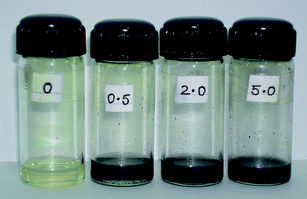 |
| | Fig. 6 Digital photograph of the PFO–MWNT solution blends with varying weight percentage of MWNTs (0%, 0.5%, 2.0%, 5.0%). | |
Fig. 7(a) and (b) show the low and high magnification SEM images respectively of the polymer PFO dissolved in toluene spin coated on ITO coated glass substrate. It can be observed that the polymer forms short fibrils which extend all over the film. This fine structure of PFO imparts a larger surface area to the polymer film than would be present in a solid, homogeneous polymer film.12 A MWNT network itself has a huge surface area (considering the high surface-to-volume ratio of carbon nanotubes). The PFO coated MWNT network will have a still larger surface area than a MWNT-only network, considering the morphology of PFO, as is visible from the SEM micrographs. However, the structure of PFO is modified on interaction with MWNTs. PFO loses its fibrilar structure and acquires a glassy, flowing kind of morphology. This is evident from the SEM micrographs shown in Fig. 8(a) and (b). Fig. 8(a) and (b) show the low and high magnification SEM images respectively of PFO coated MWNT networks.
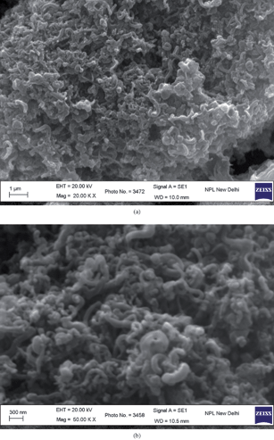 |
| | Fig. 7 (a) Low; and (b) high magnification SEM image of PFO dissolved in toluene spin coated onto an ITO-coated glass substrate. | |
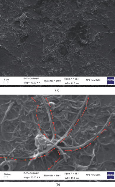 |
| | Fig. 8 (a) Low; and (b) high magnification SEM image of PFO coated MWNT networks formed from PFO + 1.0% MWNTs solution blend spin coated on ITO coated glass substrate (The arrows denote the multiple current pathways visible from one end of the film to another). | |
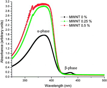
It can be observed that the obtained PFO coated MWNT networks show the presence of individually isolated and polymer coated multiwall carbon nanotubes. That the tubes are polymer coated; this fact is evidenced by the thickness of nanotubes visible in Fig. 8(b). The as-synthesized MWNTs have diameters in the range of 30–50 nm whereas in Fig. 8(b), the diameter of individual MWNT is 100–125 nm. This suggests a polymer coating of ∼75–95 nm. Also, multiple current pathways are available from one end of the film to another (as shown by arrows in Fig. 8(b)), thus showing the fault tolerance ability (breaking of a conducting path leaves many others open)16 and flexibility of the formed MWNT network. In fact, the obtained PFO coated MWNT network resembles a nanonet16 type structure. Apart from solving the dispersion problem, the polymer support adds rigidity to the formed MWNT network. It also ensures that the established carbon nanotube current pathways are maintained when subsequent layers are deposited on top of the PFO coated MWNT network layer; for example, when fabricating an organic light emitting diode (OLED) structure (in organic electronic devices such as OLEDs, OPVs, OTFTs, etc., the MWNT network layer is incorporated as an electrode or charge transporting layer). A bare MWNT network structure is more amenable to buckling under the weight of an overdeposited layer, and thus changing the initially available current pathways. The deposition of subsequent layers can lead to many broken current pathways. Moreover, in organic electronic devices, such as OLEDs, it is important to prevent the carbon nanotubes from protruding out from the film,5 in order to avoid direct contact between the nanotube and the metal electrode. Nanotubes protruding from a film can cause a short circuit due to their high conductivity. In this polymer assisted approach, even if nanotubes protrude out from the film, the chances of short circuit are comparatively less considering the fact that the protruding nanotubes are also coated with polymer and hence, instead of a nanotube–metal electrode contact, it would be a nanotube–polymer–metal electrode contact that would come into the picture. The change in conformation of the polymer PFO, on interaction with MWNTs, as evidenced by SEM micrographs, is also supported by absorption spectra. Fig. 9 shows the optical absorption spectra of PFO dissolved in toluene and PFO–MWNT solution blends with varying MWNT concentration.
It can be observed that the PFO + MWNT (0%) solution exhibits both alpha (385 nm) and beta (436 nm) phases. PFO exhibits, in addition to the regular, glassy (α-) phase, a second phase called the β-phase.17 The β-phase formation is a result of the crystallization of the n-alkyl side-chains forcing the polymer main chains into a more coplanar arrangement of the fluorene building blocks, resulting in an increased Π-conjugation along the polyfluorene main-chain.17 Thus, the PFO + MWNT (0%) solution shows a disordered glassy α phase as well as an ordered partially crystalline β phase.18 The addition of MWNTs increases absorption and also causes broadening of the polymers' characteristic absorption peak (385 nm). Fig. 10 shows a magnified view of the beta phase in the optical absorption spectra of PFO–MWNT solution blends with varying MWNT concentration. It can be observed that the beta phase peak undergoes a very high diminution on addition of MWNTs. The absorption increase can be understood considering the absorbing nature of MWNTs. The very high diminution of the beta phase peak indicates a transformation from a mix of partially crystalline and glassy structure to an almost completely disordered glassy structure. It also shows that the effective conjugation length of the polymer changes in the presence of MWNTs. Thus, MWNTs modify the local nanoscopic structure of PFO leading to a more disordered structure. The beta phase formation has also been associated with aggregation in concentrated polymer solutions.19 Hence, absence of polymer in beta phase in the PFO–MWNT solution blends indicates absence of aggregates in the PFO–MWNT solution blends and existence of more flowing kind of morphology, consistent with the SEM micrographs. This observation lends support to the conclusion that modification of MWNTs with PFO units endows MWNTs with slightly better solubility and dispersibility in toluene (absence of aggregates). The small spike in the absorption spectra of polymer–nanotube solution blends may be because of the fact that for the same amount of dilution in all three cases, the solution having carbon nanotubes will be more concentrated as compared to the polymer only solution. Fig. 11 shows the PL spectra of PFO–MWNT solution blends with varying MWNT concentration.
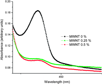 |
| | Fig. 10 Magnified view of the beta phase in the optical absorption spectra of PFO–MWNT solution blends with varying MWNT concentration. | |
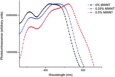 |
| | Fig. 11 PL spectra of PFO–MWNT solution blends with varying MWNT concentration. | |
The PL spectra show a well-resolved vibronic structure, with the 0–0 peak of PFO at 428 nm and 0–1 peak at 455 nm.20 These peaks are due to intrinsic properties of PFO. The addition of MWNTs in the solution blends slightly quenches the main emission peak at 428 nm. Also, a bathochromic shift in the peak at 455 nm is observed. This may be because of a change in the effective conjugation length of the conjugated polymer in the presence of nanotubes. This shift can also be because of the change in environment of the polymer chains. The polymer chains are no longer surrounded by other polymer chains or by solvent molecules. This results in the modification of the dielectric environment of conjugated polymer chains. According to the ab initio calculations which suggest that the energy levels of oligomers are substantially affected by the dielectric constant of the surrounding solvent,21 the diversified dielectric environment experienced by polymer chains may contribute to the observed bathochromic shift.22 This effect needs to be studied further in detail. The electrical properties of these PFO–MWNT solution blends have been studied using I–V characterization; and determination of percolation threshold for these PFO coated MWNT networks.
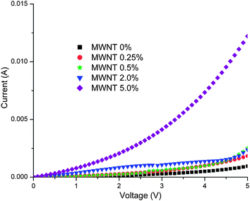
From the I–V characteristics (Fig. 12) for the schematic sandwich geometry structure shown in Fig. 1, we can observe that as the concentration of MWNTs in the PFO–MWNT solution blends increases, the threshold voltage reduces considerably (from 2.5 V for pure PFO case to 1 V for the 5% MWNT case). Also, current increases when MWNTs are incorporated in the system as compared to the pristine case. For an applied voltage of 1 V, in the 0% MWNT + PFO case, the current value is 5.5981 × 10⁻⁵ A, whereas in the 5% MWNT + PFO case, it is 7.6726 × 10⁻⁴ A, or an increase in current by one order of magnitude. This is expected considering the high electrical conductivity of carbon nanotubes. Thus, it can be inferred that, resistance of the nanocomposite is reduced with increase in MWNT concentration. The reduction in resistance leads to an increase in the current density of the pixels in the sandwich geometry structure at the same drive voltage, which may contribute to the lower turn-on voltage of the nanocomposite film based sandwich geometry structure. The observed phenomena from the I–V characteristics can be understood considering the fact that as the concentration of MWNTs in the film increases, more conducting pathways are established and more carbon nanotube–carbon nanotube junctions are formed, thus providing a large number of electrical pathways from one end of the film to another, for the charge carriers. As compared to the polymer, carbon nanotubes provide a lower resistance path to the charge carriers and hence, as soon as lower resistance electrical pathways become available, the current in the network jumps significantly above the initial value. Moreover, as mentioned by Gruner,23 for a network with substantial randomness, the conductivity is concentration dependent. More insight into the conductivity behaviour of the prepared PFO–MWNT solution blends is provided by the study of electrical percolation behaviour in these PFO coated MWNT networks.
 |
| | Fig. 12
I–V Characteristics for the schematic sandwich geometry structure shown in Fig. 1. | |
A mathematical fit to the experimental data, of the form of σ = C(f − fc)t (where f > fc) provides the electrical percolation threshold fc = 0.45 wt% and critical exponent t = 1.84 [Fig. 13]. The critical exponent's value is near to the universal value for a three-dimensional percolating system (t = 1.94),24 thus signifying the formation of a three dimensional PFO coated MWNT network. Percolation corresponds to the formation of a carbon nanotube network that allows electron transport by tunneling or electron hopping along carbon nanotube interconnects.25–27 The low value of electrical percolation threshold (0.45 wt%) obtained is a useful characteristic with regard to the polymer coated MWNT network. Hence, a continuous conductive network is formed at very low MWNT concentration, because of the high aspect ratio of the nanotubes used in this study.
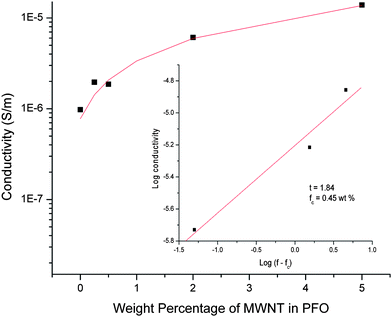 |
| | Fig. 13 Variation of electrical conductivity as a function of MWNT weight percentage in PFO coated MWNT networks. | |
4. Conclusion
Multiwall carbon nanotubes have been added to the polymer PFO in various weight percentages and the PFO–MWNT blends thus prepared, using a solution processing approach, have been characterized using SEM, UV-VIS spectroscopy, PL spectroscopy and I–V characterization. The SEM micrographs show a change in the structure of the polymer from partially crystalline to a glassy state in the blend form. The morphology observations are supported by absorption spectra which show a very high diminution of the polymers' beta peak in the spectra obtained from the polymer–nanotube blend. Thus, multiwall carbon nanotubes modify the local nanoscopic structure of PFO leading to a more glassy structure instead of partially crystalline form and provide a method to tailor the conformation of polymer PFO, depending on the intended application. I–V curves reveal an increase in current on formation of polymer–nanotube blend as compared to the polymer-only structure. On the basis of percolation theory, as applied to these polymer–nanotube blends, an electrical percolation threshold value of 0.45 wt% and critical exponent value of 1.84 has been obtained, indicating the formation of a three dimensional polymer–nanotube network. Thus, addition of MWNTs to the polymer PFO significantly changes its morphological, optical and electrical properties. These modified properties can be utilized in suitable applications, depending on the intended use.
Acknowledgements
One of the authors (M. B.) acknowledges the fellowship support (Teaching-cum-Research Fellowship) from Netaji Subhas Institute of Technology, New Delhi, India.
References
- Malti Bansal, R. Srivastava, C. Lal, M. N. Kamalasanan and L. S. Tanwar, Low electrical percolation threshold and PL quenching in solution blended MWNT/MEH PPV nanocomposites, J. Exp. Nanosci., 2010 DOI:10.1080/17458080903583980.
- Malti Bansal, R. Srivastava, C. Lal, M. N. Kamalasanan and L. S. Tanwar, Morphological, optical and electrical characterization of solution-processed MWNT/PEDOT
![[thin space (1/6-em)]](https://www.rsc.org/images/entities/char_2009.gif) :
:![[thin space (1/6-em)]](https://www.rsc.org/images/entities/char_2009.gif) PSS nanocomposite, Int. J. Mod. Phys. B, 2010 Search PubMed , in press.
PSS nanocomposite, Int. J. Mod. Phys. B, 2010 Search PubMed , in press.
- Seamus A. Curran, Pulickel M. Ajayan, Werner J. Blau, David L. Carroll, Johnathan N. Coleman, Alan B. Dalton, Andrew P. Davey, Anna Drury, Brendan McCarthy, Stephanie Maier and Adam Strevens, A Composite from poly(m-phenylenevinylene-co-2,5-dioctoxy-p-phenylenevinylene) and carbon nanotubes: A novel material for molecular optoelectronics, Adv. Mater., 1998, 10, 1091–93 CrossRef CAS.
- Jae-Yoo Kim, Moonhee Kim and Jong-Ho Choi, Characterization of light emitting devices based on a single-walled carbon nanotube–polymer composite, Synth. Met., 2003, 139, 565–68 CrossRef CAS.
- Malti Bansal, R. Srivastava, C. Lal, M. N. Kamalasanan and L. S. Tanwar, Carbon nanotube based organic light emitting diodes, Nanoscale, 2009, 1, 317–330 RSC.
- H. Ago, K. Petritsch, M. S. P. Shaffer, A. H. Windle and R. H. Friend, Composites of carbon nanotubes and conjugated polymers for photovoltaic devices, Adv. Mater., 1999, 11, 1281–85 CrossRef CAS.
- N. Izard, S. Kazaoui, K. Hata, T. Okazaki, T. Saito, S. Iijima and N. Minami, Semiconductor-enriched single wall carbon nanotube networks applied to field effect transistors, Appl. Phys. Lett., 2008, 92, 243112 CrossRef.
- Sean M. O'Flaherty, Robert Murphy, Stephanie V. Hold, Martin Cadek, Jonathan N. Coleman and Werner J. Blau, Material investigation and optical limiting properties of carbon nanotube and nanoparticle dispersions, J. Phys. Chem. B, 2003, 107, 958–64 CrossRef CAS.
-
Mark Hughes, Carbon nanotube-conducting polymer composites in supercapacitors, Dekker Encyclopedia of Nanoscience and Nanotechnology, 2nd edn, Taylor & Francis Search PubMed.
- K. H. An, S. Y. Jeong, H. R. Hwang and Y. H. Lee, Enhanced sensitivity of a gas sensor incorporating single-walled carbon nanotube–polypyrrole nanocomposites, Adv. Mater., 2004, 16, 1005–09 CrossRef CAS.
-
S. Gamerith, C. Gadermaier, U. Scherf, E. J. W. List, The origin of the green emission in polyfluorene type polymers, in Physics of Organic Semiconductors, ed. W. Brutting, Wiley-VCH Verlag, Weinheim 2005 Search PubMed.
- L. Valentini, F. Mengoni, L. Mattiello and J. M. Kenny, Electrodeposition of polyfluorene on a carbon nanotube electrode, Nanotechnology, 2007, 18, 115702 CrossRef.
- Ross A. Hatton, Anthony J. Miller and S. R. P. Silva, Carbon nanotubes: a multi-functional material for organic optoelectronics, J. Mater. Chem., 2008, 18, 1183–92 RSC.
- Malti Bansal, C. Lal, R. Srivastava, M. N. Kamalasanan and L. S. Tanwar, Comparison of structure and yield of multiwall carbon nanotubes produced by the CVD technique and a water assisted method, Phys. B, 2010, 405, 1745 CrossRef CAS.
- American Dye Source, Inc. Product Bulletin, Light emitting homopolymer for OLED & PLED devices ADS129BE.
- G. Gruner, Carbon nanonets spark new electronics, Sci. Am., 2007, 296, 76–83 CAS.
-
S. Gamerith, C. Gadermaier, U. Scherf, E. J. W. List, The origin of the green emission band in polyfluorene type polymers, in Physics of Organic Semiconductors, ed. W. Brutting, Wiley-VCH Verlag GmbH & Co., Weinheim, 2005 Search PubMed.
- M. M. Alam and S. A. Jenekhe, Binary blends of polymer semiconductors: nanocrystalline morphology retards energy transfer and facilitates efficient white electroluminescence, Macromol. Rapid Commun., 2006, 27, 2053–59 CrossRef CAS.
- C. C. Kitts and D. A. V. Bout, The effect of solvent quality on the chain morphology in solutions of poly(9,9′-dioctylfluorene), Polymer, 2007, 48, 2322–30 CrossRef CAS.
-
C. Gadermaier, L. Luer, A. Gambetta, T. Virgili, M. Z. Rossi, and G. Lanzani, Photophysics in semiconducting polymers: The case of polyfluorenes, in Semiconducting Polymers: Chemistry, Physics and Engineering, 2nd edn, ed. G. Hadziioannou and G. G. Malliaras, Wiley-VCH Verlag GmbH & Co., Weinheim, 2007 Search PubMed.
- Jolanta B. Lagowski,
Ab initio investigation of conformational and excitation energies of phenylene vinylene oligomers, THEOCHEM, 2002, 589–590, 125–137 CrossRef.
- G. Chen and P. Wang, Alteration of the optical properties of poly 9,9′-dioctylfluorene by TiO2 nanocrystalline, J. Non-Cryst. Solids, 2006, 352, 2536–38 CrossRef CAS.
- G. Gruner, Carbon nanotube films for transparent and plastic electronics, J. Mater. Chem., 2006, 16, 3533–39 RSC.
-
D Stauffer. In Introduction to Percolation Theory, Taylor & Francis, London, 1985 Search PubMed.
- Arun K. Kota, Bani H. Cipriano, Dan Powell, Srinivasa R. Raghavan and Hugh A. Bruck, Quantitative characterization of the formation of an interpenetrating phase composite in polystyrene from the percolation of multiwalled carbon nanotubes, Nanotechnology, 2007, 18, 505705 CrossRef.
- Z.-M. Dang, L. Wang, Y. Yin, Q. Zhang and Q.-Q. Lei, Giant dielectric permittivities in functionalized carbon-nanotube/electroactive-polymer Nanocomposites, Adv. Mater., 2007, 19, 852–57 CrossRef CAS.
- Lan Wang and Zhi-Min Dang, Carbon nanotube composites with high dielectric constant at low percolation threshold, Appl. Phys. Lett., 2005, 87, 042903 CrossRef.
|
| This journal is © The Royal Society of Chemistry 2010 |
Click here to see how this site uses Cookies. View our privacy policy here. ![[thin space (1/6-em)]](https://www.rsc.org/images/entities/char_2009.gif) :
:![[thin space (1/6-em)]](https://www.rsc.org/images/entities/char_2009.gif) poly(styrenesulfonic acid) (PEDOT
poly(styrenesulfonic acid) (PEDOT![[thin space (1/6-em)]](https://www.rsc.org/images/entities/char_2009.gif) :
:![[thin space (1/6-em)]](https://www.rsc.org/images/entities/char_2009.gif) PSS) was obtained from Sigma Aldrich (Product No. 483095–250G). PEDOT
PSS) was obtained from Sigma Aldrich (Product No. 483095–250G). PEDOT![[thin space (1/6-em)]](https://www.rsc.org/images/entities/char_2009.gif) :
:![[thin space (1/6-em)]](https://www.rsc.org/images/entities/char_2009.gif) PSS was filtered using a Durapore PVDF membrane filter with a pore size of 0.45 μm. ITO coated glass substrates (25 mm × 25 mm, Rs = 20 Ω/□) having ITO thickness of 120 nm, were procured from Vin Karola, USA. These were patterned and then cleaned sequentially using a non-ionic detergent solution, distilled water, acetone, trichloroethylene and propanol respectively. After baking in vacuum oven for 30 min at 120 °C, a PEDOT
PSS was filtered using a Durapore PVDF membrane filter with a pore size of 0.45 μm. ITO coated glass substrates (25 mm × 25 mm, Rs = 20 Ω/□) having ITO thickness of 120 nm, were procured from Vin Karola, USA. These were patterned and then cleaned sequentially using a non-ionic detergent solution, distilled water, acetone, trichloroethylene and propanol respectively. After baking in vacuum oven for 30 min at 120 °C, a PEDOT![[thin space (1/6-em)]](https://www.rsc.org/images/entities/char_2009.gif) :
:![[thin space (1/6-em)]](https://www.rsc.org/images/entities/char_2009.gif) PSS layer was applied to these substrates, using a spin coating unit (SCU 2007 A Apex Instruments Co.), at 2000 rpm for 2 min. The thickness of the PEDOT
PSS layer was applied to these substrates, using a spin coating unit (SCU 2007 A Apex Instruments Co.), at 2000 rpm for 2 min. The thickness of the PEDOT![[thin space (1/6-em)]](https://www.rsc.org/images/entities/char_2009.gif) :
:![[thin space (1/6-em)]](https://www.rsc.org/images/entities/char_2009.gif) PSS layer was 100 ± 5 nm, as measured using an ellipsometer (J. A. Wollam Co. M-2000U). The PEDOT
PSS layer was 100 ± 5 nm, as measured using an ellipsometer (J. A. Wollam Co. M-2000U). The PEDOT![[thin space (1/6-em)]](https://www.rsc.org/images/entities/char_2009.gif) :
:![[thin space (1/6-em)]](https://www.rsc.org/images/entities/char_2009.gif) PSS layer was applied as a buffer layer. It improves the quality of the ITO electrode by minimizing the surface roughness of ITO and reducing the resistance between polymer layer and ITO. The PEDOT
PSS layer was applied as a buffer layer. It improves the quality of the ITO electrode by minimizing the surface roughness of ITO and reducing the resistance between polymer layer and ITO. The PEDOT![[thin space (1/6-em)]](https://www.rsc.org/images/entities/char_2009.gif) :
:![[thin space (1/6-em)]](https://www.rsc.org/images/entities/char_2009.gif) PSS coated substrates were baked in a vacuum oven at 120 °C for 2 h. After that, the substrates were cooled down to room temperature and PFO–MWNT solution blends with varying weight percentages of MWNTs (0%, 0.25%, 0.5%, 2.0% and 5.0%) were applied to different substrates using a spin coating unit, at 2000 rpm for 2 min. The thickness of the PFO–MWNT blend layer was 200 ± 10 nm, as measured using an ellipsometer. The solution blend coated substrates were baked in vacuum oven at 150 °C for 2 h and then allowed to cool down to room temperature. Subsequently, aluminium electrodes were deposited by vacuum evaporation technique. A schematic diagram which illustrates the structure is shown in Fig. 1.
PSS coated substrates were baked in a vacuum oven at 120 °C for 2 h. After that, the substrates were cooled down to room temperature and PFO–MWNT solution blends with varying weight percentages of MWNTs (0%, 0.25%, 0.5%, 2.0% and 5.0%) were applied to different substrates using a spin coating unit, at 2000 rpm for 2 min. The thickness of the PFO–MWNT blend layer was 200 ± 10 nm, as measured using an ellipsometer. The solution blend coated substrates were baked in vacuum oven at 150 °C for 2 h and then allowed to cool down to room temperature. Subsequently, aluminium electrodes were deposited by vacuum evaporation technique. A schematic diagram which illustrates the structure is shown in Fig. 1.





![[thin space (1/6-em)]](https://www.rsc.org/images/entities/char_2009.gif) :
:![[thin space (1/6-em)]](https://www.rsc.org/images/entities/char_2009.gif) PSS nanocomposite, Int. J. Mod. Phys. B, 2010 Search PubMed , in press.
PSS nanocomposite, Int. J. Mod. Phys. B, 2010 Search PubMed , in press.