Effect of substrate temperature on implantation doping of Co in CdS nanocrystalline thin films
S.
Chandramohan
ad,
A.
Kanjilal
b,
S. N.
Sarangi
a,
S.
Majumder
a,
R.
Sathyamoorthy
c,
C.-H.
Hong
d and
T.
Som
*a
aInstitute of Physics, Sachivalaya Marg, Bhubaneswar, 751 005, India. E-mail: tsom@iopb.res.in; Fax: +91-674-2300142; Tel: +91-674-2301058
bInstitute of Ion Beam Physics and Materials Research, Forschungszentrum Dresden-Rossendorf, 01328, Dresden, Germany
cDepartment of Physics, Kongunadu Arts & Science College, Coimbatore, 641 029, India
dSchool of Semiconductor and Chemical Engineering, Chonbuk National University, Chonju, 561-756, South Korea
First published on 25th May 2010
Abstract
We demonstrate doping of nanocrystalline CdS thin films with Co ions by ion implantation at an elevated temperature of 573 K. The modifications caused in structural and optical properties of these films are investigated. Co-doping does not lead to amorphization or formation of any secondary phase precipitate for dopant concentrations in the range of 0.34–10.8 at.% used in the present study. However, we observe a systematic reduction in the d-spacing with increasing cobalt concentration. Optical band gap of CdS does not show any obvious change upon Co-doping. In addition, implantation gives rise to grain growth and increase in the surface roughness. The results are discussed in the light of ion-matter interaction in the keV regime.
1. Introduction
Cadmium sulfide (CdS) is recognized as one of the most promising materials in II–VI family, because of its inherent properties such as direct wide bandgap (2.43 eV at room temperature) and high luminescence efficiency in the green spectral range. Consequently, it has been implemented in various electronic and optoelectronic devices such as solar cells, light emitting diodes, lasers, thin film transistors, etc.1 Furthermore, CdS has gained another dimension as a diluted magnetic semiconductor, where a fraction of component ions of semiconductors are replaced by transition metal (TM) impurities. Recently, the research in this direction has gained renewed interest as it offers the possibility to integrate electrical, optical, and magnetic properties into a single material. In this perspective, growth of TM-doped CdS in various forms (thin films, nanoparticles, nanowires, quantum dots) has been widely demonstrated.2–6 In fact, these experimental findings verified the occurrence of various phenomena viz. reproducible bistable switching, room temperature (RT) ferromagnetism, and magneto-photoluminescence, upon doping CdS with TM (particularly Mn, Fe, Ni, and Co) impurities. Despite these significant achievements, TM-doping has been shown to alter the inherent properties of CdS, namely the change in conductivity type,7 and the persistent photoconductivity.8 To date, an extensive amount of work has been devoted to the synthesis of Mn-doped CdS; however, studies on the equally important system of Co-doped CdS are inadequate to review the potential of this system for device applications. Thus, we make an attempt to synthesize Co-doped CdS nanocrystalline thin films and study its characteristics. Growth of thin films in nanocrystalline form is advantageous because it offers extraordinary optical and electronic properties on account of small grain size and large surface-area-to-volume ratio.Several approaches have been proposed for the synthesis of TM-doped CdS, which includes electrodeposition, co-evaporation, sputtering, chemical vapour deposition, spray pyrolysis, and other different chemical routes.2–8 In contrast, ion implantation offers exceptional control and reproducibility during introduction of dopants into a semiconductor. In addition, being a non-equilibrium process, there is no solubility constraint and hence doping with high impurity concentrations can be achieved.9 However, ion implantation introduces lattice disorder and extended defects regardless of the pronounced dynamic annealing process, which as a consequence produces changes in structural, optical, and other physical properties of materials.10–12 Thus, to electrically and optically activate the dopants, it is necessary to remove the lattice damage generated during the implantation process by a suitable thermal annealing procedure.
The use of nanocrystalline thin films (where every grain of the film is a nanocrystalline one and of few tens of nm in size) have several advantages over other forms of doping by means of ion implantation. Due to the small dimensionality of nanometre sized grains and numerous interfaces between adjacent crystallites, it is likely that the spread in energy loss during ion implantation is confined to small regions.13,14 This would result in coalescence of particles at the near-surface regions, which is paramount for improving the electromigrative characteristics of thin film devices.14 In this paper, we discuss modifications in structural, morphological, and optical properties of nanocrystalline CdS films due to Co-doping by implantation at elevated temperature. The results of our investigation prove that Co-ion implantation at 573 K leads to good solubility of the dopant without inducing any secondary phase formation or amorphization. However, Co-doping does not lead to any modification in the band gap. Further, implantation leads to enhancement in the surface roughness and grain growth. In addition, we address the effect of substrate temperature during implantation by comparing the results with those corresponding to RT implantation.
2. Experimental
CdS thin films (650 nm thick) were grown by thermal evaporation on micro-glass slides at a substrate temperature of 373 K. Stoichiometric films with a granular morphology were obtained by maintaining a constant and slow rate of deposition (10 nm s−1). Subsequently, the films were uniformly implanted with 90 keV Co+ ions for various fluences in the range of 0.1–3.6 × 10¹⁶ ions cm−2. These fluences correspond to the Co concentration of 0.34 to 10.8 at.% at the mean projected range. Implantation was done at an elevated temperature of 573 K in order to avoid amorphization and to enhance the solubility of Co ions in the CdS lattice. The criterion for selecting this temperature is based on the fact that a temperature above 623 K could cause a preferential removal of sulfur from CdS.15 Therefore, a temperature lower than this value was selected to avoid any detrimental effect on the film quality. Monte Carlo SRIM2008 simulation16 predicts the projected range of 90 keV Co ions in CdS to be 58.7 nm with straggling of 29.7 nm.Phase analysis of the pristine and the Co-doped CdS films was performed by glancing angle X-ray diffraction (GAXRD) using Cu Kα radiation (λ = 0.154 nm). Atomic force microscopy (AFM) measurements were performed in the tapping mode. The optical transmittance measurements were carried out by using an ultraviolet-visible-near-infrared (UV-Vis-NIR) spectrophotometer. The photoluminescence (PL) spectra were acquired by exciting the samples with a He–Cd laser (325 nm) at 10 K. Micro-Raman measurements were performed at RT in a backscattering geometry by using the 532.14 nm line of Nd:YAG laser excitation. The laser power was maintained at a lower value of 0.2 mW to avoid laser induced heating of the sample.
3. Results and discussion
Fig. 1 shows the GAXRD patterns of pristine and Co-ion implanted CdS films. The pristine film is polycrystalline in nature and the observed peak positions match well with the hexagonal close packed (hcp) wurtzite structure of CdS.17 The crystallites are observed to have grown preferentially along the c-axis direction, which has the lowest surface energy in the wurtzite structure. It is observed that the polycrystalline nature of the pristine film is retained even after Co-ion implantation at the highest fluence. This indicates that CdS can be considered as a reasonably good radiation-resistant material. However, Co-ion implantation leads to slight broadening in the line width of the (002) peak. In general, broadening takes place either when crystallites become smaller or if lattice defects or strain are present in the film.18 In the present case, we rule out the possibility of reduction in the crystallite size since from our AFM studies we observe a definite grain growth (described later). Thus, the observed line broadening can be attributed to the result of Co-doping induced lattice disorder and related effects caused during implantation.11 However, the amount of broadening is comparatively lesser than that observed for Co-doped CdS at RT. Thus, high temperature implantation is advantageous to control the ion induced lattice disorder.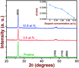 | ||
| Fig. 1 GAXRD patterns of the pristine and the Co-doped nanocrystalline CdS thin films for dopant concentrations of 3.88 and 10.8 at.%. The inset shows variation in the lattice d-spacing as a function of dopant concentration. | ||
We also observe a systematic reduction in the lattice d-spacing for the (002) plane with increasing Co-ion concentration (inset of Fig. 1). The observed lattice contraction implies that the incorporated Co atoms, with smaller ionic radii, are likely to occupy the substitutional cationic sites in the CdS lattice. This could give rise to the building up of strain in the lattice which can cause X-ray line broadening (as discussed above). These results are quite consistent with those reported for Co-doped CdS systems, prepared by conventional methods.6,19 We do not observe formation of any metallic clusters or secondary phase precipitates unlike a previous report on ion implanted CdS systems.15 This could be due to the supersaturation of implanted ions occupying the substitutional cationic sites as discussed above.
The effect of Co-doping on the optical properties of CdS is studied by using spectral transmittance data. The direct band gap, Eg, of CdS was estimated from the (αhυ)2versus photon energy (hυ) plot as shown in Fig. 2. The band gap of the pristine CdS film was found to be 2.39 eV, which is close to the value reported in the literature for evaporated films.10 No appreciable change in Eg was observed for entire range of Co concentrations used in this study. In addition, the fundamental absorption edge becomes steep indicating an improvement in the crystalline quality of the films after Co-doping. To further validate these results, PL measurements were carried out on the pristine and the Co-doped CdS films. Typical emission spectra of CdS films before and after Co-ion implantation are illustrated in Fig. 3.
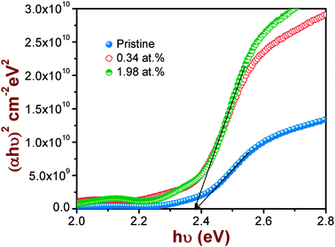 | ||
| Fig. 2 Plot of (αhυ)2versus hυ showing the estimation of direct band gap energy as a function of dopant concentration. | ||
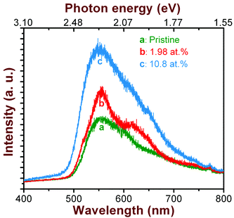 | ||
| Fig. 3 Photoluminescence spectra (at 10 K) of CdS thin films before and after cobalt doping at different concentrations. | ||
The spectrum acquired from the pristine CdS film shows two emission bands centred around 2.23 eV and the other one at 1.9 eV. The higher energy emission at 2.23 eV is known as the yellow emission band, which is associated with radiative transitions from the donor levels, arising due to Cd atoms at the interstitial sites (ICd), to the valence band (VB).20,21 On the other hand, the shoulder-like lower energy emission at 1.9 eV is known as the orange emission band (OB), which can be attributed to complex defects such as ICd-VCd Frenkel pairs.22 In Fig. 3, we also present the PL spectra of CdS films implanted for a dopant concentration of 1.98 and 10.8 at.%. It is seen that the emission characteristics of CdS changes upon Co-doping. Here, we observe a systematic increase in the emission efficiency of the yellow band with increasing cobalt concentration, although there is no noticeable shift in the band positions. This agrees well with the optical absorption results discussed above. In other words, the fundamental band edge of CdS is not modified due to the addition of Co-ions into the CdS lattice. In contrary, Co-implantation at RT yields a decrease in the band gap due to defect-induced band tailing effect. The increase in the efficiency of yellow emission can be explained on the basis of ion-solid interaction as follows.
Interaction of ions with matter in the energy range under consideration is dominated by nuclear energy loss caused by elastic collision between incident ions and target atoms. As a result, a dense collision cascade gets developed in a solid when energetic ions travel through it. Time evolution of such a collision cascade can be divided into different phases.23 The initial stage, during which atoms collide strongly, is known as the collisional phase and has a lifetime of ∼0.1–1 ps. Due to such collisional events all atoms near the ion path are set into thermal motion at a high temperature. This high temperature spreads and reduces within the lattice by heat conduction. This is known as thermal spike phase and it lasts for ∼1 ns. As a result, a large number of defects are created in the solid. These defects can be of several types, i.e. vacancies, interstitial atoms, complex interstitial-dislocation loops, and volume defects.24,25 However, it is anticipated that the majority of these defects would be annihilated at 573 K. Nevertheless, the incorporation of Co ions into CdS would induce accumulation of uncompensated defects in the crystal lattice, which are likely to be thermally stable even at high temperatures. Based on the electron bombardment experiments performed with 100–300 keV electrons, it has been reported by Kulp26 that the threshold energy required to knock out the Cd and the S atoms from their lattice positions is 7.3 and 8.7 eV, respectively. Thus, it is easier to displace a Cd atom than an S atom in the CdS lattice. It is also worth mentioning here that the binding energy of Cd atoms is smaller than that of S atoms in the wurtzite crystal structure.27 As a result implanted Co atoms can displace Cd atoms to the interstitial positions and occupy the resultant vacancies. Therefore, the emission efficiency of the yellow band increases with increasing Co concentrations. Interestingly, the low energy emission associated with ICd-VCd complex defects is totally suppressed when the Co concentration exceeds 10 at.%. This means that the Cd vacancy sites are effectively filled up by the implanted Co ions by self-compensation process with the aid of additional thermal energy supplied to the substrate during implantation. This argument on substitution of vacant Cd sites by Co atoms is also substantiated by the GAXRD results discussed earlier.
Fig. 4 shows the micro-Raman spectra of the pristine and the Co-implanted CdS films. The peak position, full width at half maximum (FWHM), and area under the peak were deduced by fitting the experimental data with a Lorentzian line shape. The Raman modes at about 300 and 601 cm−1 observed in the pristine sample correspond to the A1 1LO and 2LO phonon modes of wurtzite CdS, respectively.27,28 The corresponding frequency of the 1LO mode in CdS crystals is reported to be 305 cm−1.27 Thus, we observe a downward peak shift of ∼5 cm−1 for the pristine sample, which can be attributed to the grain-size effect or the surface phonon mode effect due to the small dispersion of LO phonon wave vector in polycrystalline films.29 Comparing the spectra of the pristine film and those of the implanted ones, we do not observe any additional modes that are activated after Co-ion implantation. Moreover, the peak positions get shifted marginally towards lower frequency although no systematic variation with Co-ion fluence is observed. These small shifts might result due to the differences in grain size of the pristine and the Co-doped samples. However, we observe a systematic decrease in the FWHM and an increase in the peak area (under the 1LO Raman peak) with increasing Co concentration (inset in Fig. 4). A decrease in the FWHM value can be attributed to improvement in the crystalline quality of the films. It has been demonstrated for several nanocrystalline systems that the Raman line width decreases when there is an increase in the particle size.30–32 This observation is contrary to the result of Co-implanted CdS films at RT, where we observe a broadening in the line width of Raman peaks. On the other hand, the scattering intensity increases with increasing Co-ion fluence, analogous to the results observed at RT. In fact, a similar kind of enhancement in the Raman peak intensity was reported for ion implanted CdS and ZnO samples and was attributed to the change in the surface roughness.10,33 It is known that rough surfaces can enhance the light scattering cross-section.34 Our AFM measurements reveal an increase in the surface roughness with increasing ion fluence as described below.
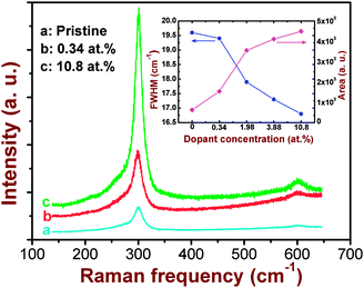 | ||
| Fig. 4 Raman spectra of the pristine and the Co+-implanted CdS films for typical dopant concentrations of 0.34 and 10.8 at.%. The inset shows variation in the FWHM and the area under the 1LO peak with dopant concentration. | ||
Fig. 5 shows the AFM images of the pristine sample and the film implanted to a Co peak concentration of 10.8 at%. It can be seen from Fig. 5(a) that the pristine sample consists of big grains which are further comprised of small nanocrystallites (∼30 nm of average size). After Co-ion implantation, the individual nanocrystallites start coalescing with each other and form bigger particles of different dimensions (up to ∼150 nm at the highest fluence) as seen from Fig. 5(b). Implantation induced grain growth has been reported for other systems as well.14,35 The reason for the ion induced grain growth can be explained within the framework of the thermal spike model described earlier. According to this, temperature spikes caused by ions and recoils induce atomic jumps across grain boundaries, promoting boundary migration.14 If a number of atoms move in one direction, the boundary moves in the opposite direction, resulting in the coalescence of grains. It may be mentioned that we observe formation of mound-like structures in the case of cobalt doping by RT implantation. This can be explained as follows. In the present case, since implantation is done at 573 K, each grain gets enough thermal energy to coalesce with the neighbouring ones to result in an enhanced grain growth. In addition, data analysis shows a systematic increase in the root-mean-square surface roughness (Rq) with increasing ion fluence. For instance, the measured value of Rq for the pristine sample is 3.8 nm, which increases up to 34.3 nm for the highest fluence. This systematic change in the surface roughness is attributed to grain growth due to cobalt implantation doping at elevated temperature. In the case of Co-doping at RT, implantation results in a similar enhancement in the surface roughness; however, a maximum value of Rq for the highest fluence was found to be 15.4 nm. Thus, it clearly indicates a two-fold enhancement in the surface roughness when implantation is performed at elevated temperature due to enhanced grain growth.
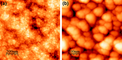 | ||
| Fig. 5 AFM images of nanocrystalline CdS thin films: (a) pristine and (b) after 10.8 at.% cobalt doping by ion implantation at elevated temperature. | ||
4. Conclusions
In summary, we have investigated the effect of substrate temperature during implantation-assisted Co-doping (0.34–10.8 at.%) of nanocrystalline CdS thin films and related modifications in structural, optical, morphological, and vibrational properties of these films. Based on our experimental observations, it is inferred that the implanted cobalt atoms occupy the substitutional sites in the CdS lattice. Besides, Co-doping does not induce formation of metallic clustering or amorphization. Doping at elevated temperature does not show any obvious change in the optical band gap unlike the films doped by cobalt implantation at RT. This behavior indicates a considerable reduction in lattice disorder due to elevated temperature doping. These results are consistent with the emission characteristics observed from the PL studies. Raman scattering studies also indicate an improvement in the crystalline quality. In addition, an increase in the surface roughness is observed due to ion induced grain growth. Thus, it may be concluded that cobalt doping of nanocrystalline CdS thin films by ion implantation at elevated temperatures would be useful for synthesis of doped CdS based devices with good structural and optical quality.Acknowledgements
We acknowledge F. Ludewig for his help in ion implantation. H. Kim (Chonbuk National University) is acknowledged for his assistance in carrying out the PL measurements. This work was supported in part by Priority Research Centers Program through the National Research Foundation of Korea (NRF) funded by the Ministry of Education, Science and Technology (2009-0094032).References
- N. V. Hullavarad, S. S. Hullavarad and P. C. Karulkar, J. Nanosci. Nanotechnol., 2008, 8, 3272 CrossRef CAS.
- J. C. Lee, N. G. Subramaniam, J. W. Lee and T. W. Kang, Appl. Phys. Lett., 2007, 90, 262909 CrossRef.
- D. H. Kim, D. J. Lee, N. M. Kim, S. J. Lee, T. W. Kang, Y. D. Woo and D. J. Fu, J. Appl. Phys., 2007, 101, 094111 CrossRef.
- C. W. Na, D. S. Han, D. S. Kim, Y. J. Kang, J. Y. Lee, J. Park, D. K. Oh, K. S. Kim and D. Kim, J. Phys. Chem. B, 2006, 110, 6699 CrossRef CAS.
- E. Bacaksiz, M. Tomakin, M. Altunbas, M. Parlak and T. Colakoglu, Phys. B, 2008, 403, 3740 CrossRef CAS.
- S. Delikanli, S. He, Y. Qin, P. Zhang, H. Zeng, H. Zhang and M. Swihart, Appl. Phys. Lett., 2008, 93, 132501 CrossRef.
- X. J. Wu, D. Z. Shen, Z. Z. Zhang, J. Y. Zhang, K. W. Liu, B. H. Li, Y. M. Lu, D. X. Zhao and B. Yao, Appl. Phys. Lett., 2006, 89, 262118 CrossRef.
- N. Badera, B. Godbole, S. B. Srivastava, P. N. Vishwakarma, L. S. S. Chandra, D. Jain, M. Gangrade, T. Shripathi, V. G. Sathe and V. Ganesan, Appl. Surf. Sci., 2008, 254, 7042 CrossRef CAS.
- N. Akdogan, H. Zabel, A. Nefedov, K. Westerholt, H.-W. Becker, S. Gök, R. Khaibullin and L. Tagirov, J. Appl. Phys., 2009, 105, 043907 CrossRef.
- K. Senthil, D. Mangalaraj, Sa. K. Narayandass, B. Hong, Y. Roh, C. S. Park and J. Yi, Semicond. Sci. Technol., 2002, 17, 97 CrossRef CAS.
- Mendoza-Galván, C. Trejo-Cruz, J. Lee, D. Bhattacharyya, J. Metson, P. J. Evans and U. Pal, J. Appl. Phys., 2006, 99, 014306 CrossRef.
- S. Chandramohan, A. Kanjilal, S. N. Sarangi, S. Majumder, R. Sathyamoorthy and T. Som, J. Appl. Phys., 2009, 106, 063506 CrossRef.
- R. R. Ahire, A. A. Sagade, N. G. Deshpande, S. D. Chavhan, R. Sharma and F. Singh, J. Phys. D: Appl. Phys., 2007, 40, 4850 CrossRef CAS.
- D. E. Alexander and G. S. Was, Phys. Rev. B: Condens. Matter, 1993, 47, 2983 CrossRef CAS.
- H. Metin and R. Esen, Semicond. Sci. Technol., 2003, 18, 647 CrossRef CAS.
- J. F. Zeigler, J. P. Biersack and U. Littmark, The Stopping and Range of Ions in Solids, Pergamon, New York, 1985, vol. 1 Search PubMed; http://www.srim.org/ .
- Powder Diffraction File # 77-2306, ICDD, JCPDS-International Centre for Diffraction DataNewton Square, PA, 1997 Search PubMed.
- T. Ungar, Scr. Mater., 2004, 51, 777 CrossRef CAS.
- K. A. Bogle, S. Ghosh, S. D. Dhole, V. N. Bhoraskar, L.-F. Fu, M.-F. Chi, N. D. Browning, D. Kundaliya, G. P. Das and S. B. Ogale, Chem. Mater., 2008, 20, 440 CrossRef CAS.
- C. T. Tsai, D. S. Chuu, G. L. Chen and S. L. Yang, J. Appl. Phys., 1996, 79, 9105 CrossRef CAS.
- B.-S. Moon, J.-H. Lee and H. Jung, Thin Solid Films, 2006, 511–512, 299 CrossRef CAS.
- O. Vigil, I. Riech, M. Garcia-Rocha and O. Zelaya-Angel, J. Vac. Sci. Technol., A, 1997, 15, 2282 CrossRef CAS.
- W. Bolse, Mater. Sci. Eng., R, 1994, 12, 53.
- K. Saarinen, P. Hautojärvi, J. Keionen, E. Rauhala, J. Räisänen and C. Corbel, Phys. Rev. B: Condens. Matter, 1991, 43, 4249 CrossRef CAS.
- T. Diaz de la Rubia and M. Guinan, Phys. Rev. Lett., 1991, 66, 2766 CrossRef CAS.
- B. A. Kulp, Phys. Rev., 1962, 125, 1865 CrossRef CAS.
- H. Khallaf, G. Chai, O. Lupan, L. Chow, S. Park and A. Schulte, J. Phys. D: Appl. Phys., 2008, 41, 185304 CrossRef.
- H. Pan, G. Xing, Z. Ni, W. Ji, Y. P. Feng, Z. Tang, D. H. C. Chua, J. Lin and Z. Shen, Appl. Phys. Lett., 2007, 91, 193105 CrossRef.
- D. S. Chuu and C. M. Dai, Phys. Rev. B: Condens. Matter, 1992, 45, 11805 CrossRef CAS.
- D. Bersani, P. P. Lottici and Xing-Zhao Ding, Appl. Phys. Lett., 1998, 72, 73 CrossRef CAS.
- L. Zeiri, I. Patla, S. Acharya, Y. Golan and S. Efrima, J. Phys. Chem. C, 2007, 111, 11843 CrossRef CAS.
- V. Swamy, A. Kuznetsov, L. S. Dubrovinsky, R. A. Caruso, D. G. Shchukin and B. C. Muddle, Phys. Rev. B: Condens. Matter Mater. Phys., 2005, 71, 184302 CrossRef.
- J. D. Ye, S. Tripathy, F.-F. Ren, X. W. Sun, G. Q. Lo and K. L. Teo, Appl. Phys. Lett., 2009, 94, 011913 CrossRef.
- J. R. Molina-Contreras, C. Medina-Gutierrez, C. Frausto-Reyes, R. Trejo-Vazquez, F. J. Villalobos-Pina, G. Romo-Luevano and S. Calixto, J. Phys. D: Appl. Phys., 2007, 40, 4922 CrossRef CAS.
- B. Pandey, S. Ghosh, P. Srivastava, P. Kumar and D. Kanjilal, J. Appl. Phys., 2009, 105, 033909 CrossRef.
| This journal is © The Royal Society of Chemistry 2010 |
