Pt surface modification of SnO2 nanorod arrays for CO and H2 sensors
Hui
Huang
*a,
C. Y.
Ong
a,
J.
Guo
b,
T.
White
bc,
M. S.
Tse
a and
O. K.
Tan
a
aMicroelectronics Centre, School of Electrical and Electronic Engineering, Nanyang Technological University, 50 Nanyang Avenue, 639798, Singapore. E-mail: hhuang@ntu.edu.sg; Fax: +65 6793 3318
bSchool of Materials Science and Engineering, Nanyang Technological University, 50 Nanyang Avenue, 639798, Singapore
cCentre for Advanced Microscopy, Australian National University, Sullivan’s Creek Road, Canberra ACT 2601,
Australia
First published on 19th May 2010
Abstract
Uniform SnO2 nanorod arrays were deposited on a 4 inch SiO2/Si wafer by plasma-enhanced chemical vapor deposition (PEVCD) at low deposition temperature of around 300 °C. The SnO2 nanorods were connected at the roots, thus the nanorod sensors could be fabricated by a feasible way compatible with microelectronic processes. The surface of the sensors was modified by Pt nanoparticles deposited by dip coating and sputtering, respectively. The sensing properties of the Pt-modified SnO2 nanorod sensors to CO and H2 gases were comparatively studied. After surface modification of Pt, the sensing response to CO and H2 gases increased dramatically. The 2 nm Pt-modified SnO2 nanorod sensors by sputtering showed the best sensing performance. By increasing Pt thickness from 2 nm up to 20 nm, the optimal working temperature decreased by 30 °C while the sensing response also decreased by about 4 times. Comparing these two Pt modification approaches by dip coating and sputtering, both could achieve comparable promotion effect if the Pt thickness can be controlled around its optimal value. The deposition technique of SnO2 nanorod arrays by PECVD has good potential for scale-up and the fabrication process of nanorod sensors possesses simplicity and good compatibility with contemporary microelectronics-based technology.
1. Introduction
Nanotechnology has opened up the possibilities of producing sensing materials in the form of quasi one-dimensional (1D) nanostructures like nanobelts, nanowires, nanotubes, and nanorods.1–4 The conductivity of the 1D nanostructures could vary from a fully non-conductive state to a highly conductive state entirely on the basis of the surface chemistry. Their peculiar characteristics and size effects make them potential candidates as the third generation of gas sensors. For the gas sensors detecting reducing and toxic gases, SnO2 was one of the first considered, and still is the most frequently used material. Recently, various SnO2 1D nanostructures were fabricated and applied to gas sensors.5–8 These 1D nanostructures show good sensing performance, but most synthesis techniques reported produce either dispersed or randomly oriented assemblies of the 1D SnO2 nanostructures.9–13 These disordered 1D SnO2 nanostructures are too minute to handle during the preparation of sensor devices14 and the reliability of these sensor devices is not investigated and doubtful.Various strategies have been proposed as possible solutions by creating arrays of 1D SnO2 nanostructures, with most of the reported work utilizing template-assisted methods. For example, SnO2 nanowire arrays were fabricated by Zheng et al.15 using electrochemical deposition and thermal oxidizing methods based on highly ordered nanoporous alumina membrane (AAM). The diameter of SnO2 nanowires is about 70 nm, which is basically equal to that of pores of the AAM used. Wu and Lu16 fabricated arrays of nanoporous tin oxide nanorods by electrodeposition of tin into AAM followed by anodization of tin nanorods to create nanochannels. Kolmakov et al.8 reported a new paradigm for producing SnO2 nanowire sensor arrays with possibly thousands of addressable sensing elements by oxidation of Sn nanowires. SnO2 nanohole arrays have been prepared by Hamaguchi et al.17 using a liquid phase deposition method. The SnO2 nanohole array sensors equipped with noble metal (Pt, Pd, and Au) electrodes exhibited reversible response to H2 gas in air. Among the electrode materials used, the largest response was achieved with Pd and the maximum value of sensitivity was 187 at 350 °C.
The integration of individual or arrays of 1D nanostructures with planar technology still poses a major challenge for the mass production of gas sensors at reasonably low cost. To become a successful third generation gas sensor, the 1D nanostructures and their sensors, must be grown and fabricated in a manner that possesses the characteristics of simplicity, versatility and good compatibility with contemporary microelectronics-based technology. In addition, the nanostructured sensors show poor selectivity to specific gases. Surface functionalization is critical to improve the sensitivity and selectivity of the nanostructured sensors.
In this paper, SnO2 nanorod arrays were deposited on a 4 inch SiO2/Si wafer by PECVD at low deposition temperature. SnO2 nanorod sensors were fabricated by a feasible way compatible with microelectronic processes. The surface was modified by Pt nanocrystals using both chemical and physical deposition techniques. The sensing properties of the Pt-modified SnO2 nanorod sensors to CO and H2 gases were comparatively studied.
2. Results and discussion
Fig. 1(a) shows the XRD patterns of the nanorod arrays grown on a 4 inch SiO2/Si substrate by PECVD for 2 h. The as-deposited nanorods were well crystallized even without substrate heating. The substrate was heated by the plasma and the substrate temperature was stabilized at around 300 °C after 1.2 kW plasma 2 h deposition. All diffraction peaks can be indexed by Cassiterite SnO2 (PDF 41-1445). The SnO2 nanorods are very uniform in size and spacial distribution (Fig. 1(b)) and fully cover the whole area of the 4 inch wafer. The nanorods grow directly on the SiO2/Si substrate and randomly stretch out (Fig. 1(c)).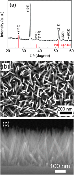 | ||
| Fig. 1 (a) XRD patterns, (b) planar SEM image and (c) cross-sectional SEM image of the SnO2 nanorod arrays grown on a 4 inch SiO2/Si wafer by PECVD for 2 h. | ||
The TEM image (Fig. 2(a)) of the SnO2 nanorods shows that the SnO2 nanorods are about 5 nm at the tip, 20 nm at the bottom and 300 nm in length. The nanorods were connected together at the roots by a thin SnO2 seed layer. The SnO2 nanorod arrays have high spatial distribution density. Calculated from Fig. 1(b) and Fig. 2(a), the spatial distribution density is about 2.78 × 10¹⁴ m−2 and the surface area of the nanorod arrays in 1 μm2 substrate area is 3.5 μm2. The clear lattice fringes shown in the HRTEM image (Fig. 2(b)) indicate that each nanorod is a single crystal. The lattice spacing measured in Fig. 2(b) is 3.6 Å and 2.7 Å, corresponding to (110) and (101) plane of tetragonal SnO2 (P42/mnm) with lattice parameters of a = 3.187 Å and b = c = 4.738 Å, respectively, which is consistent with the XRD measurement (Fig. 1(a)).
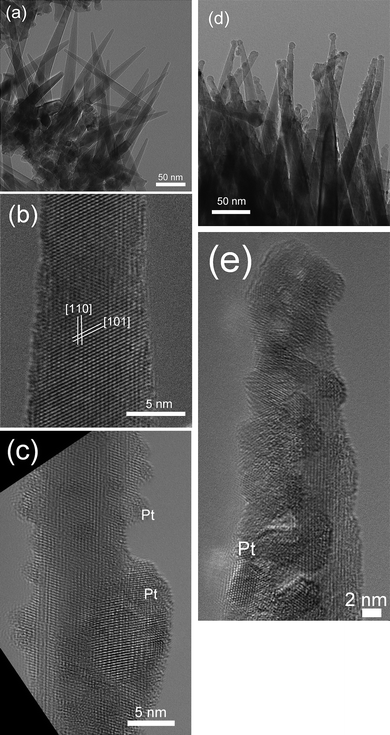 | ||
| Fig. 2 Bright field TEM images of pristine and Pt-modified SnO2 nanorods deposited by PECVD: (a) SnO2 nanorod arrays; (b) single SnO2 nanorod; (c) Pt-modified SnO2 nanorods by dip coating for 15 min; (d) 2 nm Pt-modified SnO2 nanorods by sputtering and (e) one typical Pt-modified SnO2 nanorod by sputtering. | ||
The surface of the SnO2 nanorods was modified by Pt deposited by dip coating and sputtering. The Pt nanoparticles deposited by dip coating for 15 min are around 1–3 nm in diameter while some large agglomerated Pt particles were also observed (Fig. 2(c)). The Pt concentration detected by X-ray photoelectron spectroscopy (XPS) analysis was 1.6 atm%. After sputtering 2 nm Pt on the nanorod, some large Pt nanoparticles can be observed on the tips of the nanorods (Fig. 2(d)). Due to the shadow effect during the sputtering, the Pt deposited on the nanorods is thicker on the deposition side and thin on the shadowed side (Fig. 2(d) and 2(e)). From the HRTEM shown in Fig. 2(e), the Pt nanocrystals deposited by sputtering are about 2–5 nm in diameter. The Pt concentration of the 2 nm Pt-modified SnO2 nanorods detected by XPS analysis was 2.7 atm%.
The sensing responses as a function of working temperatures of Pt-modified SnO2 nanorod sensors by dip coating to 1000 ppm CO and H2 gas in dry air are summarized in Fig. 3. The as-deposited pristine SnO2 nanorod sensor showed low sensing response to both CO and H2 gases. After annealing, the oxygen vacancies in the nanorods reduced, and thus the sensing response dropped as well. Obviously, the Pt-modified SnO2 nanorod sensors showed much higher sensing response than the unmodified sensors. The sensing responses of the Pt-modified sensors reach their maxima at an optimal working temperature of around 400 °C. Typically, the Pt-modified sensor by dip coating for 15 min showed an 11-fold and 4-fold better sensor response for 1000 ppm CO and H2 gases, respectively, than the unmodified sensor. With prolonged dipping times up to 48 h, the sensing response reached its maximum for both CO and H2 gases. The improvement on the sensing response of the Pt-doped sensors was ascribed to the effect of “chemical sensitization mechanism” proposed by Yamazoe et al.18 The Pt nanoparticles promote the reaction of the H2 gases with oxygen species adsorbed on the surface of SnO2 nanorods by a “spillover” effect,10 leading to an enhancement of the sensing response and also a decrease of operating temperature. Gaidi et al.19 indicated further that a spillover effect predominates at high operating temperature while an electronic effect is responsible at low temperature. The sensing response to CO gas is mainly due to the change of Pt from the oxidation state to the reduced one.20
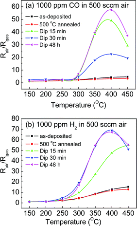 | ||
| Fig. 3 Sensing response to (a) 1000 ppm CO and (b) 1000 ppm H2 as a function of working temperatures of Pt-modified SnO2 nanorod sensors by dip coating. | ||
The SnO2 nanorod sensor was also modified by the thickness of Pt from 2 nm to 20 nm deposited by sputtering. The sensing response to 1000 ppm CO and H2 gases are shown in Fig. 4. Among all the sensors, the 2 nm Pt-modified SnO2 nanorod sensor achieved its highest sensing response at an optimal working temperature of 405 °C. Particularly, the H2 gas sensing response of 262 is 5 times than that of CO gas, which indicates that the sensor shows high selectivity to H2 gas. As discussed earlier, Pt surface modification increased the sensing response by a spillover effect. In this case, the Pt thickness is critical for gas response since the spillover of the activated sample gas facilitates a chemical reaction with the negatively charged oxygen adsorbed on the SnO2 surface to produce CO2 and H2O.21
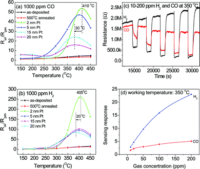 | ||
| Fig. 4 Sensing properties of Pt-modified SnO2 nanorod sensors by sputtering: (a) response to 1000 ppm CO, (b) response to 1000 ppm H2, (c) consecutive responses to 10–200 ppm H2 and CO gas and (d) sensing response vs. concentrations of 2 nm Pt-modified SnO2 nanorod sensors. | ||
The effect of Pt thickness on the sensing response is also studied. With increasing the Pt thickness up to 20 nm, the optimal working temperature decreased by 30 °C while the sensing response decreased by about 4 times. Excessive Pt modification will form a quasi-continuous Pt layer on the surface of SnO2 nanorods, which diminishes the interfacial area between sensor and target gas and thus slows down gas diffusion and reactions on the surface of SnO2 nanorods. Eventually, the sensing response is degraded with increasing Pt thickness (up to 20 nm) (Fig. 4(a) and 4(b)). The results indicate that 2 nm Pt modification is optimal for maximum sensing response of the SnO2 nanorod sensors. Gaidi et al.19 also reported that 3 atm% Pt concentration was optimal for CO gas. Comparing these two Pt modification approaches, we believe that both can achieve comparable promotion effect if the Pt thickness can be controlled around its optimal value of 2 nm (2.7 atm%) in this study. Fig. 4(c) and 4(d) show the sensing response of the 2 nm Pt-modified SnO2 nanorod sensors to 10 ppm to 200 ppm H2 and CO gases, respectively. The sensor showed repeatable and reversible response and even 10 ppm H2 and CO can be detected by the Pt-modified SnO2 nanorod sensors with good sensitivity of 2.85 and 1.63, respectively. The sensor shows much higher sensing response to H2 than CO gas (Fig. 4(d)), indicating a better selectivity to H2.
3. Conclusions
In this paper, uniform SnO2 nanorod arrays have been grown by PECVD at very low deposition temperature of around 300 °C. SnO2 nanorod sensors were fabricated and the pristine sensors showed a low response to CO and H2 gases. After the surface modification of Pt by dip coating, the sensing response to CO and H2 gases increased drastically. The 2 nm Pt-modified SnO2 nanorod sensors by sputtering showed the best sensing performance. With increasing Pt thickness from 2 nm up to 20 nm, the optimal working temperature decreased by 30 °C while the sensing response also decreased by about 4 times. 2 nm of Pt modification is optimal for maximum sensing response of the SnO2 nanorod sensors. Comparing these two Pt modification approaches by dip coating and sputtering, both could achieve comparable promotion effect if the Pt thickness can be controlled around its optimal value, 2 nm in this study.4. Experimental
The SnO2 nanorod arrays were deposited in a custom-designed horizontal inductively coupled PEVCD and the deposition details are described elsewhere.22 Briefly, dibutyltin diacetate (Aldrich, 98% purity) was used as the tin precursor. Ar was used as the carrier gas and O2 was used as the reaction gas. The Ar/O2 plasma was generated by a 1.2 kW RF generator. The 4 inch wafer was put vertically in a quartz boat and no additional substrate heating was applied during deposition. After deposition, the SnO2 nanorod arrays were modified by Pt using dip coating and sputtering, respectively. The SnO2 nanorod arrays were dipped in 0.01 M H2PtCl6·6H2O solution for 15 min to 48 h and then dried with N2 blowing. Various thickness from 2 nm to 20 nm Pt was deposited on the SnO2 nanorods by sputtering. All the samples were annealed at 500 °C for 1 h in air.The crystal structure of the SnO2 nanorod arrays was detected by a Siemens D5005 X-ray diffractometer (XRD) with Cu-Kα radiation. A Leo 1550 field emission scanning electron microscope (FE-SEM) was used to observe the morphologies of the SnO2 nanorod arrays. The microstructure of the nanorods was studied by a JEOL JEM-2010F transmission electron microscope (TEM). The chemical structures of the samples were analyzed on a VG ESCALAB 220-IXL X-ray photoelectron spectroscopy with an Al Kα X-ray source (1486.6 eV photons) operated at 300 W.
The fabrication procedures of the nanorod sensors are schematically shown in Fig. 5. Au inter-digital top electrodes were deposited on the SnO2 nanorods by electron beam evaporation using shadow mask. For purpose of characterization and measurements, the SnO2 nanorod sensor devices were attached to alumina substrates and the interdigital gold electrodes were connected to the respective gold pads on the alumina using gold wire bonding. Gas sensing properties were characterized using a computer-controlled gas sensing characterization system. The programs for the measuring procedures were designed using the National Instruments' LABVIEW. The operating temperature was up to 450 °C achieved using a 1 inch Linkam heater stage. Before testing, an air sweep from room temperature to 450 °C with a heating rate of 1 °C min−1 was carried out to condition the device. Next, the device was heated to 450 °C step by step with a heating rate of 1 °C min−1. At each temperature step, test gas was introduced into the chamber with dry air while maintaining the total combined flow rate of 500 sccm. The flow rate and concentration of test gas were controlled using four MKS MFCs. A Keithley 236 source measure unit was used for the direct current–voltage measurement. The gas sensing response S is defined by the relative resistance, S = Rair/Rgas, where Rair and Rgas are the resistance of the sensor in air and in detecting gas respectively.
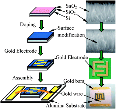 | ||
| Fig. 5 Fabrication procedure for the Pt-modified SnO2 nanorod sensors. | ||
Acknowledgements
H. Huang thanks the LKY PDF Start-up Grant (Grant No. LKY 3/08) for financial support.References
- Z. R. Dai, J. L. Gole, J. D. Stout and Z. L. Wang, J. Phys. Chem. B, 2002, 106, 1274–1279 CrossRef CAS.
- P. C. Chen, G. Z. Shen and C. W. Zhou, IEEE Trans. Nanotechnol., 2008, 7, 668–682 CrossRef.
- Z. L. Wang, Adv. Mater., 2003, 15, 432–436 CrossRef CAS.
- Z. R. Dai, Z. W. Pan and Z. L. Wang, Adv. Funct. Mater., 2003, 13, 9–24 CrossRef CAS.
- M. Law, H. Kind, B. Messer, F. Kim and P. Yang, Angew. Chem., Int. Ed., 2002, 41, 2405–2408 CrossRef CAS.
- L. P. Qin, J. Q. Xu, X. W. Dong, Q. Y. Pan, Z. X. Cheng, Q. Xiang and F. Li, Nanotechnology, 2008, 19, 185705 CrossRef.
- A. Maiti, J. A. Rodriguez, M. Law, P. Kung, J. R. McKinney and P. Yang, Nano Lett., 2003, 3, 1025–1028 CrossRef.
- A. Kolmakov, Y. Zhang, G. Cheng and M. Moskovits, Adv. Mater., 2003, 15, 997–1000 CrossRef CAS.
- H. Huang, Y. C. Lee, O. K. Tan, W. Zhou, N. Peng and Q. Zhang, Nanotechnology, 2009, 20, 115501 CrossRef.
- Y. Shen, T. Yamazaki, Z. F. Liu, D. Meng and T. Kikuta, J. Alloys Compd., 2009, 488, L21–L25 CrossRef CAS.
- J. D. Prades, R. Jimenez-Diaz, F. Hernandez-Ramirez, S. Barth, A. Cirera, A. Romano-Rodriguez, S. Mathur and J. R. Morante, Sens. Actuators, B, 2009, 140, 337–341 CrossRef.
- I. S. Hwang, J. K. Choi, S. J. Kim, K. Y. Dong, J. H. Kwon, B. K. Ju and J. H. Lee, Sens. Actuators, B, 2009, 142, 105–110 CrossRef.
- A. Kolmakov, D. O. Klenov, Y. Lilach, S. Stemmer and M. Moskovits, Nano Lett., 2005, 5, 667–673 CrossRef CAS.
- H. Huang, Y. C. Lee, O. K. Tan, W. Zhou, N. Peng and Q. Zhang, Nanotechnology, 2009, 20, 115501 CrossRef.
- M. Zheng, G. Li, X. Zhang, S. Huang, Y. Lei and L. Zhang, Chem. Mater., 2001, 13, 3859–3861 CrossRef CAS.
- K. H. Wu and S. Y. Lu, Electrochem. Solid-State Lett., 2005, 8, D9–D11 CrossRef CAS.
- T. Hamaguchi, N. Yabuki, M. Uno, S. Yamanaka, M. Egashira, Y. Shimizu and T. Hyodo, Sens. Actuators, B, 2006, 113, 852–856 CrossRef.
- N. Yamazoe, Y. Kurokawa and T. Seiyama, Sens. Actuators, 1983, 4, 283–289 CrossRef CAS.
- M. Gaidi, J. L. Hazemann, I. Matko, B. Chenevier, M. Rumyantseva, A. Gaskov and M. Labeau, J. Electrochem. Soc., 2000, 147, 3131–3138 CrossRef CAS.
- M. Gaidi, B. Chenevier, M. Labeau and J. L. Hazemann, Sens. Actuators, B, 2006, 120, 313–315 CrossRef.
- B. K. Min and S. D. Choi, Sens. Actuators, B, 2005, 108, 119–124 CrossRef.
- Y. C. Lee, O. K. Tan, H. Huang, M. S. Tse and H. W. Lau, IEEE Trans. Nanotechnol., 2007, 6, 465–468 CrossRef.
| This journal is © The Royal Society of Chemistry 2010 |
