Donor–acceptor polymers for advanced memory device applications
Cheng-Liang
Liu
*a and
Wen-Chang
Chen
*b
aDepartment of Organic Device Engineering, Yamagata University, Yonezawa, Yamagata 992-8510, Japan. E-mail: clliu@yz.yamagata-u.ac.jp; Fax: +81-23-826-3309; Tel: +81-23-826-3309
bDepartment of Chemical Engineering and Institute of Polymer Science and Engineering, National Taiwan University, Taipei, Taiwan 106. E-mail: chenwc@ntu.edu.tw; Fax: +886-2-3366-5237; Tel: +886-2-3366-5236
First published on 9th June 2011
Abstract
Organic materials for memory devices have attracted significant scientific interest recently due to the advantages of rich structure flexibility, low cost, solution processability, and three-dimensional stacking capability. This minireview highlights the recent developments in donor–acceptor polymers for resistive switching memory device applications including conjugated polymers, functional polyimides, non-conjugated pendent polymers, and polymer composites. It emphasizes the structure-memory characteristic relationship of donor–acceptor polymers for advanced memory device applications.
 Cheng-Liang Liu | Cheng-Liang Liu received his BS and PhD in Chemical Engineering from National Taiwan University in 2002 and 2007, respectively. He joined the group of Professor Wen-Chang Chen in 2001 and meanwhile performed research as a visiting scientist at University of Washington under the guidance of Professor Samson A. Jenekhe from 2006 to 2007. He then became a Post-doctoral Fellow in the group of Professor Wen-Chang Chen in 2008. In 2010, he accepted the position of Assistant Professor at the Department of Organic Device Engineering of Yamagata University (Japan), mentored by Professor Junji Kido. His research interests include organic electronics especially in memory devices. |
 Wen-Chang Chen | Wen-Chang Chen is a Professor in the Department of Chemical Engineering, Distinguished Professor and Director of Polymer Science and Engineering at the National Taiwan University. He received a PhD degree in Chemical Engineering from the University of Rochester in 1993 and then served at a research scientist at the Industrial Technology Research Institute of Taiwan from 1993 to 1996. He joined the National Taiwan University as an Associate Professor in 1996. His current research activities include electronic and optoelectronic polymers, block copolymers, and hybrid materials. He has co-authored 184 refereed articles and 22 issued patents. |
Introduction
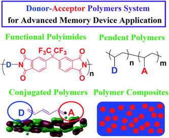
The resistive-type memory cell has a capacitor-like structure containing organic polymer materials1–3 or metal oxide4 sandwiched between two metal electrodes that efficiently store the data based on the current response to an applied voltage. The write operation is performed by applying a voltage bias or pulse to the device, which results in the reversible or irreversible switching between the high-resistance (OFF) and low-resistance (ON) state. As the transition occurs, the device remains in one of the two states after turning off the power that determines the volatility of data storage. The erase process is performed by the applications of appropriate voltage in the same polarity (unipolarity) or reverse voltage (bipolarity). Simple memory cells based on metal–insulator–metal (MIM) geometry, highly scalable cross-point and multilevel stacking architecture have been fabricated.3Donor–acceptor (D–A) type polymers have been the subject of much research in recent years due to their promising applications in light-emitting diodes,5 field effect transistors,6 solar cells,7 and memory devices.1–3 In particular, D–A polymer-based memory devices with an electrically bistable behavior have received considerable attention recently due to the attractive characteristics such as rich structure flexibility, low cost, solution processability, and three-dimensional stacking capability. Device incorporating switchable D–A polymeric elements are classified as follows: conjugated polymers,8–17 functional polyimides (PIs),2,18–33 non-conjugated pendent polymers34–41 and polymer composites (metal nanoparticles (NPs)1,42 or fullerene derivatives1,43–46 embedded), as shown in Fig. 1. Moreover, electronic memory devices can be generally divided into two categories, namely non-volatile memory (write-once-read-many times (WORM) memory, flash (rewritable) memory or switching with negative differential resistance (NDR) behavior) and volatile memory (dynamic random access memory (DRAM) or static random access memory (SRAM)) according to the device volatility.3 Some models for the driving mechanism of resistive switching have been illustrated such as charge transfer (CT) effect, conductive filament formation and trapping/detrapping of charge.3 This minireview focuses on the recent advances directed towards the molecular structures, memory characteristics and switching mechanism of memory devices based on the D–A polymer systems. Also, we present a concluding outlook on the molecular design of D–A type polymer memory materials.
 | ||
| Fig. 1 Molecular structures of donor–acceptor polymer systems for advanced memory device applications. | ||
Conjugated polymers
Memory devices from fluorene-based D–A conjugated copolymers (PFOxPy) were demonstrated in the literature.8–12PFOxPy containing oxadizole and bipyridine as acceptor units fulfilled the functionality of a volatile DRAM due to the short retention ability of ON state current.8 The memory behavior was elucidated from space charge and traps. Turning off power caused detrapping of the filled traps due to the shallow site of filled traps.8 However, other fluorene–acceptor push–pull polymeric system (such as F12TPN9) performed the non-volatile nature.9–12F12TPN consisting of fluorene and pendent triphenylamine (TPA) donors and pyridine acceptors exhibited the WORM memory behavior.9 The injected hole could migrate through the continuous positive electrostatic potential channel along the polymer chain and become trapped by the nitrogen atom of the pyridine acceptors. The filled traps could not be detrapped easily by the reverse voltage bias, leading to the WORM behavior of F12TPN.9 Besides, the device based on conjugated poly[9,9-bis(4-diphenylaminophenyl)-2,7-fluorene] donors covalently bridged with Disperse Red 1 acceptors (DR1-PDPAF-DR1) exhibited an accessible rewritable memory characteristic.10 The excitation of donor promoted CT to the conjugated channel, finally the electrons were at LUMO1 or further at LUMO2 and gave rise to a conductive charge separation state.10 Non-volatile tristable memory effects were demonstrated in the polyfluorene-diphenylpyridine copolymers with pendent carbazole groups.11 Effective charge transport channel for hopping between the ordered structures switched the device from OFF to ON-1 state as evidenced by in situfluorescence emission spectra and high resolution of TEM image.11 The enhanced absorption of the polymer film was consistent with the interfacial CT interaction at the polymer/ITO interface that elucidated the switching transition from ON-1 to ON-2 state.11 Polyfluorene-based copolymers containing the side-chain electron-rich TPA and electron-poor cyano substituents exhibited a typical WORM memory characteristic since the positive charges on the TPA or fluorene moieties were rapidly consumed by the cyano groups as a result of switching operation.12Non-volatile switching characteristic with NDR using conjugated copolymers of poly(3-hexylthiophene) (P3HT)-block-poly(2-phenyl-5-(4-vinylphenyl)-1,3,4-oxadiazole) (POXD) were shown to efficiently store the data based on the high- and low-conductance response to an applied voltage (Fig. 2).13 Multi-level electronic states depended on the charge hopping conduction between the P3HT blocks and the deep charge traps in the POXD blocks. The combined self-assembly nature of ordered conjugated rod-coil block copolymers and relative energy level of D–A system led to the nano-scale polymer memory device applications.13
 | ||
| Fig. 2 Poly(3-hexylthiophene)-block-poly(vinylphenyl oxadiazole) donor–acceptor rod–coil block copolymers and their memory device applications. Reprinted with permission from ref. 13. Copyright 2010 Wiley-VCH Verlag GmbH & Co. KGaA. | ||
Electrically switching materials based on modified D–A functionalized conjugated polymer complex systems could be converted by the application of an electric field.14–17 Conjugated polyfluorene chelated with electron-withdrawing europium (Eu) or iridium (Ir) complex were selected as the active memory materials, namely PFEu14 and iamp,15 respectively. The PFEu device showed a WORM memory characteristic even with different substituted alkyl chains or composition ratio14 whereas iamp showed a flash memory.15 The non-volatile behavior may be probably attributed to the polarized effect of positively charged fluorene units and negative charged Eu or Ir complex forming a conducting channel for charge carriers.14,15 Higuchi and his coworkers also tuned the non-volatile bipolar switching behavior viacobalt (Co)-containing conjugated polymers with an extended azo aromatic ligand (Co(III)-Azo CP).16Redox switching of hybrid polymers generated bistable states with an ON/OFF ratio of 103. The results of cyclic voltammograms and direct switching response of the device indicated that the switching phenomenon were due to the reduction of Co ion in the conjugated polymers.16 TPA-based conjugated polyazomethine covalently grafted with graphene oxide (TPAPAM-GO) was directly used to fabricate non-volatile rewritable memory devices.17 Electrons transmitted from the HOMO of the hole transporting polymer TPAPAM into LUMO of graphene layervia intramolecular CT interaction established charge transport pathways and switched the device from the OFF to ON state. The effective electron delocalization in graphene nanosheets might stabilize the CT state of TPAPAM-GO, leading to a non-volatile nature.17
In general, the incorporation of different electron acceptors into conjugated polymeric donors significantly affects the memory properties, which can either create a trapping environment or provide the CT conducting channel in the electrical switching. The stability of charge trapping or CT complex process determines the volatility of memory device.
Functional polyimides
Functional aromatic polyimides (PIs, Chart 1) are promising materials for microelectronic device applications due to their excellent physical and chemical properties. Recently, significant research activities have been invested in the development of all types of PI switching behaviors. Functional PIs containing both electron donors and acceptors within a single macromolecule contributed to electronic transition between the ground and excited state, which could be manipulated by the induced CT from donor to acceptor under applied electric fields. For example, TPA moieties as electron donors were proposed to enhance the electron donating and charge transport ability with the phthalimide acceptor.18 PI(TP6F) with TPA moieties exhibited DRAM behavior18 while PI(PYTPA) (containing combined donor effects from TPA and diphenylpyridine) showed improved DRAM performance.19 Meanwhile, the memory characteristics of PI(6F-2TPA) (two connected TPA rings) exhibited stable digital nonvolatile WORM and volatile DRAM memory characteristics depending on the film thickness.20 Besides, a flash-type memory of PI(6F-HAB-TPAIE) bearing two pendent TPA groups21 and a unipolar WORM memory of PI(6F-HTPA) with an attached hydroxyl group on the TPA groups22 were also reported. The mono- or dual-mediated phenoxy linkages (L) between the TPA and phthalimide moieties, represented as (D–L–A)n (PI(AAPT-6FDA)) and (L–D–L–A)n (PI(APT-6FDA)), were found to significantly affect the volatile behaviors that exhibited DRAM and SRAM behavior, respectively.23 Both PI(OXTA)24 or PI(AZTA)25 containing TPA-substituted 1,3,4-oxadiazole or triazole moieties were prepared for the WORM memory device.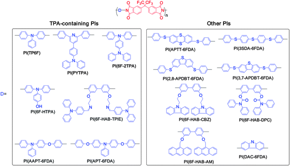 | ||
| Chart 1 Chemical structures of functional polyimides for memory devices. | ||
The switching phenomena of PIs can be further modified with donor–acceptor strength. The relatively higher dipole moments of sulfur-containing PI(APTT-6FDA) and PI(3SDA-6FDA) showed the nonvolatile flash memory characteristics.26 However, the comparable weak dipole moments of dibenzothiophene-containing PIs (PI(2,8-APDBT-6FDA) or PI(3,7-APDBT-6FDA)) probably led to unstable CT complex for the DRAM device.27 A switching device based on PI(BPPO), containing 2,5-bis(4-phenoxyphenyl)-1,3,4-oxadiazole (BPPO) moieties as the electron donors and phthalimide moieties as the electron acceptors, was observed with the SRAM characteristic.28 The thermally and dimensionally stable PI(6F-HAB-CBZ)29 or PI(6F-HAB-DPC)30 or (PI(6F-HAB-AM)31 with the carbazole or diphenylcarbamyloxy or anthracene moieties in the side groups were also fabricated for electrically bistable non-volatile switching devices. Different from the non-volatile PIs with pendent donors, PI(DAC-6FDA) with both electron-donating carbazole and electron-accepting phthalimide located in the main chain provided DRAM properties.32PI(BTFBPD-DPBPDA) and PI(BTFBPD-BTFBPDA) bearing a non-coplanar twisted biphenyl unit with aromatic side-chain groups exhibited a flash and WORM type memory behavior, respectively.33
Kang and coworkers first proposed that the switching mechanism was supported by the electric-field induced CT effect as evidenced by molecular simulation or fluorescence quenching.2,18,19,28 The threshold voltage of memory devices depends on the relative energy barrier between the HOMO energy level and work function of metal electrode.2,26 The electrical stability of the induced CT complex after removal of the electric field was further dominated by dipole moment of the D–A PIs.2,18,19,23,26,28 Following the above CT process, PIs also underwent chain twisting under the applied electric field. The more torsional conformation in the excited state produced a potential barrier that prevented the recombination of separated charges and delayed the back CT process, which possibly explained the comparative maintenance of ON state current.23,25,28,33 However, the trap-limited space-charge-limited-current (SCLC) conduction and local filament formation represented another electrical switching mechanism, where the traps came from the donors (act as nucleophilic sites) and acceptors (electrophilic sites) depending on the association.20,21,29–31 The PIs with donor and acceptor structures on the main chain weakened the charge-trapping ability and made the space charge generated in molecules easily be neutralized after removal of the applied voltage.21,32 Correspondingly, this device returned to its OFF state immediately and exhibited the volatile effect.32 However, electron donor and acceptor power of PIs could be retained or increased if the donor moieties were a side group21 or the stronger electron-donating moieties were directly included in the materials22 and thus non-volatile memory devices were obtained.
Non-conjugated pendent polymers
The materials based on side-chain type D–A species in the backbone were also favorable for the performance of memory devices. The carbazole groups were widely used in the molecular design of electron-donating and hole transporting materials and the corresponding memory effect was observed by introducing suitable acceptors in the molecules. Kang and coworkers designed the non-conjugated copolymers containing pendent carbazole donor and Eu complex acceptor (PKEu) that could meet the requirement of non-volatile electrically bistable memory devices.34 Besides this, the additional incorporation of the pendent 1,3,4-oxdiazole (Ox) block into methacrylate copolymer consisting of a carbazole and Eu complex (named as PCzOxEu) exhibited a significant improvement in performance under ambient conditions.35 As the voltage reaches the threshold, the resultant CT complex with the increased number of free charge carriers (mainly holes hopping between the neighboring carbazole units) switched the device to the high conducting state.34,35 The large dipole moment of the Ox component acted as a mediator to reduce the internal energy barrier and facilitate carrier transport, which favored the holding of the separated charges for the longer retention time with improved device stability.35The electrical bistable switching behavior of the pendent D–A polymer devices was affected by both the electronic structure and surface morphology.36 The electron-withdrawing dispersed red 1 (DR1)-functionalized PVK copolymers (PVDK) were fabricated for memory device as the active layer sandwiched between ITO and Al electrode.36PVDR film displayed helical columnar stacks with large grain sizes, whereas a non-aggregated PVDR film exhibited an amorphous morphology with a smaller grain size.36 Both the PVDR devices showed WORM performance with an ON/OFF current ratio of 105.36 The asymmetric distribution of the HOMO and LUMO level could stabilize the conductive CT state of the PVDR copolymer leading to the non-volatile and non-erasable behavior. Besides, the stability of the nano-aggregated PVDR device was much better than that of the non-aggregated PVDR device. The surface defects and large numbers of the grain boundaries in the amorphous PVDR sample acted as charge trapping centers. An effective charge transport channel and better polymer/metal contacts of the self-assembled smooth PVDR film contributed to the more stable ON state current in the corresponding device.36 Similar WORM devices were constructed from two PVK derivatives with the pendent azobenzene chromopheres and terminal electron acceptor moieties (–NO2 or –CN).37 Electric field-formed high dipole moments originally from increased charge separation upon CT led to the non-volatile behavior.37
Recently, we developed the pendent polymers containing electron-donating carbozole units (VPK) and electron-withdrawing oxadiazole-containing units (OXD or BOXD) with different D/A ratios for memory device applications (Fig. 3).38 The low-lying HOMO energy level of OXD or BOXD units as compared to VPK units created the trapping environment. Therefore, distinct electrical characteristics changed between the diode, volatile memory, and insulator depending on the relative D/A ratios. The unstable ON state of volatile nature SRAM in the P(VPK8OXD2) or P(VPK8BOXD2) device was due to the shallow trapped holes with spontaneous back transferring of charge carriers when the electric field was removed.38 Besides, the tunable switching behaviors were explored through the different ratio of pendent TPA donors and BOXD acceptors.41 The relative extent of charge trapping/spontaneously back-transferring of trapped carriers controlled the switching behavior. The additional cyano side groups in the pendent TPA donors exhibited NDR behavior probably due to the preferred interaction of the Al atoms with the cyano group.41
 | ||
| Fig. 3 Donor–acceptor random copolymers with pendent triphenyamine and 1,3,4-oxidazole for memory device applications. Reprinted with permission from ref. 41. Copyright 2011 American Chemical Society. | ||
Non-conjugated homopolymers with pendent D–A systems in the azobenzene chromophores exhibited a different memory performance.39,40 The reversibility of charge trapping and thus the volatility of memory effect were determined by the strength of the donors and acceptors and dependence on the terminal moiety of the azobenzene.39,40 Therefore, the WORM memory effect was observed in memory devices based on the pendant azobenzene chromophores containing nitro or bromo (acceptor) terminal moieties such as AzoNO2,39 AzoNEtNO2,39 AzoNEtBr,39 PNAzo40 and PBAzo,40 while the flash type memory effect was observed in those based on pendant chromophores containing methoxy (donor) terminal moieties such as AzoOOCH3,39AzoNEtOCH339 and PMAzo.40 In the OFF state, the device current was low since injected holes were trapped while hopping along the pendant azobenzene chromophores. At the switching voltage, the majority of the traps were filled and a trap-free environment with higher charge mobility was formed.39 Large permanent dipole moments of the pendent azobenzene-based polymers with the D–A structures created internal electric field to maintain the high conductivity state even the removal of the voltage bias.39 However, the rewritable flash type of azobenzene chromophores with electron donors as terminal moieties could be detrapped by reverse bias since intramolecular CT to form charge-separated states were not observed.39
Polymer composites
Although several types of single polymer devices have been demonstrated, hybrid composites were also extensively prepared for memory device applications.1,42–46 The supplementary compounds (NPs or fullerene derivatives) could be viewed as the data storage media or have the physical electronic transition with the organic polymer matrix. Yang and coworkers first proposed the memory environment consisting of a sufficient amount of well-dispersed capped-gold (Au) NPs and aromatic 8-hydroxyquinoline (8-HQ) compound within a polystyrene (PS) supporting matrix.42 The CT interaction between the 8HQ and Au-DT NPs (which can act as donor and acceptor, respectively) under a high electric field explained the electronic transition in Al/Au-DT + 8HQ + PS/Al devices.42Small molecules or/and polymers and PCBM blended composite thin film were prepared for non-volatile memory applications such as PS and tetrathiafulvalene (TTF),43P3HT,44 and poly(fluorenylstyrene)-block-poly(2-vinylpyridine) (P(St-F)-b-P2VP) block copolymers.45 The switching mechanism based on such blended composites and configuration included electric field-induced CT43,45 or polarization among the adjacent domains.44 Other blended systems based on PVK donors with carbon nanotubes (CNTs)46 were proposed for the possible applications in resistive memory materials. The doping level of PCBM or CNT content in the polymer matrix significantly affected the charge transport process and consequently had an influence on the electrical behaviors.45,46
Concluding remarks
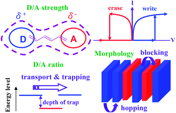
The D–A polymeric (composite) materials with the intrinsic switching behavior provide great interest because the memory characteristics could be adjusted over a wide range of modifications on chemical structures. Significant research effect in the development of polymer switching materials with excellent electrical characteristics is continuously investigated to meet the requirement of the memory devices. From the analysis of the structure–memory properties relationship, the approaches to the emerging architectures of new D–A polymers for memory devices are summarized as follows (Fig. 4):(a) Effect on D/A strength: Strong (or complete) CT between the donors and acceptors easily produces a low bandgap polymer with conducting or semiconducting properties. However, D/A polymer materials (usually carbazole or fluorine donors) with moderate (or incomplete) CT are likely to exhibit switching behaviors by external voltage bias. The strong dipole moment of molecule helps to sustain the conductive CT state and thus presents a non-volatile behavior. Otherwise, the conductive CT state is not stable and dissociates after removal of the electric field resulting in the volatile nature of the memory effect.
(b) Effect on relative ratio of D/A moieties: π-conjugated donors that allow charge transportvia a hopping process (usually polymers are p-channel conductors with a suitable choice of metal electrode) with appropriate acceptors for preparing charge-trapping condition from the relative energy level when the external voltage is applied. Sufficient loading ratio/composition of the acceptors serves as the hole-blocking moieties and interrupts the transport between the neighboring donors if there is no obvious CT or significant orbital hybridization. The optimization of donor/acceptor ratios and the depth of trapping barrier define the volatile/non-volatile nature.
(c) Effect on morphology: The suitable modulation of the D/A structures that considers the relative electronic properties followed by controllable morphology could establish the memory characteristics. The well-defined morphology on the interface between D and A moieties significantly affects the charge transporting/blocking ability for designing memory devices.
 | ||
| Fig. 4 Contributing effects of the donor–acceptor polymers on the memory switching behavior. | ||
The development of high performance organic memory devices with long-term stability relies on the appropriate molecular design, high density storage of vertical-stacked memory without sneak current path, and solution-processing on a flexible substrate. Such devices can be further integrated for promising applications such as radio frequency identification (RFID) or electronic paper.
Acknowledgements
W.-C. Chen thanks the financial support from the National Science Council of Taiwan and the Excellence Research Program of National Taiwan University. C.-L. Liu also thanks the support from the Promotion of Environmental Improvement for Independence of Young Researchers Program of Ministry of Education, Culture, Sports, Science and Technology-Japan.References
- Y. Yang, J. Ouyang, L. Ma, R. J. H. Tseng and C. W. Chu, Adv. Funct. Mater., 2006, 16, 1001 CrossRef CAS.
- Q.-D. Ling, D.-J. Liaw, E. Y.-H. Teo, C. Zhu, D. S.-H. Chan, E.-T. Kang and K.-G. Neoh, Polymer, 2007, 48, 5182 CrossRef CAS.
- Q.-D. Ling, D.-J. Liaw, C. Zhu, D. S.-H. Chan, E.-T. Kang and K.-G. Neoh, Prog. Polym. Sci., 2008, 33, 917 CrossRef CAS.
- A. Sawa, Mater. Today, 2008, 11, 28 CrossRef CAS.
- A. C. Grimsdale, K. Leok Chan, R. E. Martin, P. G. Jokisz and A. B. Holmes, Chem. Rev., 2009, 109, 897 CrossRef CAS.
- A. C. Arias, J. D. MacKenzie, I. McCulloch, J. Rivnay and A. Salleo, Chem. Rev., 2010, 110, 3 CrossRef CAS.
- Y.-J. Cheng, S.-H. Yang and C.-S. Hsu, Chem. Rev., 2009, 109, 5868 CrossRef CAS.
- Q.-D. Ling, Y. Song, S.-L. Lim, E. Y.-H. Teo, Y.-P. Tan, C. Zhu, D. S. H. Chan, D.-L. Kwong, E.-T. Kang and K.-G. Neoh, Angew. Chem., Int. Ed., 2006, 45, 2947 CrossRef CAS.
- G. Liu, Q.-D. Ling, E.-T. Kang, K.-G. Neoh, D.-J. Liaw, F.-C. Chang, C.-X. Zhu and D. S.-H. Chan, J. Appl. Phys., 2007, 102, 024502 Search PubMed.
- Q.-D. Ling, E.-T. Kang, K.-G. Neoh, Y. Chen, X.-D. Zhuang, C. Zhu and D. S. H. Chan, Appl. Phys. Lett., 2008, 92, 143302 Search PubMed.
- G. Liu, D. J. Liaw, W. Y. Lee, Q. D. Ling, C. X. Zhu, D. S. H. Chan, E. T. Kang and K. G. Neoh, Philos. Trans. R. Soc. London, Ser. A, 2009, 367, 4203 Search PubMed.
- X.-D. Zhuang, Y. Chen, B.-X. Li, D.-G. Ma, B. Zhang and Y. Li, Chem. Mater., 2010, 22, 4455 CrossRef CAS.
- Y.-K. Fang, C.-L. Liu, C. Li, C.-J. Lin, R. Mezzenga and W.-C. Chen, Adv. Funct. Mater., 2010, 20, 3012 CrossRef CAS.
- L. Li, Q.-D. Ling, S.-L. Lim, Y.-P. Tan, C. Zhu, D. S. H. Chan, E.-T. Kang and K.-G. Neoh, Org. Electron., 2007, 8, 401 CrossRef.
- S.-J. Liu, Z.-H. Lin, Q. Zhao, Y. Ma, H.-F. Shi, M.-D. Yi, Q.-D. Ling, Q.-L. Fan, C.-X. Zhu, E.-T. Kang and W. Huang, Adv. Funct. Mater., 2011, 21, 979 Search PubMed.
- A. Bandyopadhyay, S. Sahu and M. Higuchi, J. Am. Chem. Soc., 2011, 133, 1168 Search PubMed.
- X.-D. Zhuang, Y. Chen, G. Liu, P.-P. Li, C.-X. Zhu, E.-T. Kang, K.-G. Noeh, B. Zhang, J.-H. Zhu and Y.-X. Li, Adv. Mater., 2010, 22, 1731 CrossRef CAS.
- Q.-D. Ling, F.-C. Chang, Y. Song, C.-X. Zhu, D.-J. Liaw, D. S.-H. Chan, E.-T. Kang and K.-G. Neoh, J. Am. Chem. Soc., 2006, 128, 8732 CrossRef CAS.
- Y.-L. Liu, Q.-D. Ling, E.-T. Kang, K.-G. Neoh, D.-J. Liaw, K.-L. Wang, W.-T. Liou, C.-X. Zhu and D. S.-H. Chan, J. Appl. Phys., 2009, 105, 044501 CrossRef.
- T. J. Lee, C.-W. Chang, S. G. Hahm, K. Kim, S. Park, D. M. Kim, J. Kim, W.-S. Kwon, G.-S. Liou and M. Ree, Nanotechnology, 2009, 20, 135204 CrossRef.
- K. Kim, S. Park, S. G. Hahm, T. J. Lee, D. M. Kim, J. C. Kim, W. Kwon, Y.-G. Ko and M. Ree, J. Phys. Chem. B, 2009, 113, 9143 CrossRef CAS.
- D. M. Kim, S. Park, T. J. Lee, S. G. Hahm, K. Kim, J. C. Kim, W. Kwon and M. Ree, Langmuir, 2009, 25, 11713 CrossRef CAS.
- T. Kuorosawa, C.-C. Chueh, C.-L. Liu, T. Higashihara, M. Ueda and W.-C. Chen, Macromolecules, 2010, 43, 1236 CrossRef CAS.
- K.-L. Wang, Y.-L. Liu, J.-W. Lee, K.-G. Neoh and E.-T. Kang, Macromolecules, 2010, 43, 7159 CrossRef CAS.
- K.-L. Wang, Y.-L. Liu, I. H. Shih, K.-G. Neoh and E.-T. Kang, J. Polym. Sci., Part A: Polym. Chem., 2010, 48, 5790 CrossRef CAS.
- N.-H. You, C.-C. Chueh, C.-L. Liu, M. Ueda and W.-C. Chen, Macromolecules, 2009, 42, 4456 CrossRef CAS.
- C.-L. Liu, T. Kurosawa, A.-D. Yu, T. Higashihara, M. Ueda and W.-C. Chen, J. Phys. Chem. C, 2011, 115, 5930 Search PubMed.
- Y.-L. Liu, K.-L. Wang, G.-S. Huang, C.-X. Zhu, E.-S. Tok, K.-G. Neoh and E.-T. Kang, Chem. Mater., 2009, 21, 3391 CrossRef CAS.
- S. G. Hahm, S. Choi, S.-H. Hong, T. J. Lee, S. Park, D. M. Kim, W.-S. Kwon, K. Kim, O. Kim and M. Ree, Adv. Funct. Mater., 2008, 18, 3276 CrossRef CAS.
- S. G. Hahm, S. Choi, S.-H. Hong, T. J. Lee, S. Park, D. M. Kim, J. C. Kim, W. Kwon, K. Kim, M.-J. Kim, O. Kim and M. Ree, J. Mater. Chem., 2009, 19, 2207 RSC.
- S. Park, K. Kim, D. M. Kim, W. Kwon, J. Choi and M. Ree, ACS Appl. Mater. Interfaces, 2011, 3, 765 Search PubMed.
- G. Tian, D. Wu, S. Qi, Z. Wu and X. Wang, Macromol. Rapid Commun., 2011, 32, 384 Search PubMed.
- Y. Li, H. Xu, X. Tao, K. Qian, S. Fu, Y. Shen and S. Ding, J. Mater. Chem., 2011, 21, 1810 RSC.
- Q. Ling, Y. Song, S. J. Ding, C. Zhu, D. S. H. Chan, D.-L. Kwong, E.-T. Kang and K.-G. Neoh, Adv. Mater., 2005, 17, 455 CrossRef CAS.
- Q.-D. Ling, W. Wang, Y. Song, C.-X. Zhu, D. S.-H. Chan, E.-T. Kang and K.-G. Neoh, J. Phys. Chem. B, 2006, 110, 23995 CrossRef CAS.
- X.-D. Zhuang, Y. Chen, G. Liu, B. Zhang, K.-G. Neoh, E.-T. Kang, C.-X. Zhu, Y.-X. Li and L.-J. Niu, Adv. Funct. Mater., 2010, 20, 2916 CrossRef CAS.
- G. Liu, B. Zhang, Y. Chen, C.-X. Zhu, L. Zeng, D. Siu-Hung Chan, K.-G. Neoh, J. Chen and E.-T. Kang, J. Mater. Chem., 2011, 21, 6027 RSC.
- Y.-K. Fang, C.-L. Liu and W.-C. Chen, J. Mater. Chem., 2011, 21, 4778 RSC.
- S. L. Lim, N.-J. Li, J.-M. Lu, Q.-D. Ling, C. X. Zhu, E.-T. Kang and K. G. Neoh, ACS Appl. Mater. Interfaces, 2009, 1, 60 CrossRef CAS.
- N. Li, J. Lu, H. Li and E.-T. Kang, Dyes Pigm., 2011, 88, 18 Search PubMed.
- Y.-K. Fang, C.-L. Liu, G.-Y. Yang, P.-C. Chen and W.-C. Chen, Macromolecules, 2011, 44, 2604 Search PubMed.
- J. Ouyang, C.-W. Chu, C. R. Szmanda, L. Ma and Y. Yang, Nat. Mater., 2004, 3, 918 CrossRef CAS.
- C. W. Chu, J. Ouyang, J.-H. Tseng and Y. Yang, Adv. Mater., 2005, 17, 1440 CrossRef CAS.
- J. Liu, Z. Yin, X. Cao, F. Zhao, A. Lin, L. Xie, Q. Fan, F. Boey, H. Zhang and W. Huang, ACS Nano, 2010, 4, 3987 CrossRef CAS.
- J.-C. Hsu, C.-L. Liu, W.-C. Chen, K. Sugiyama and A. Hirao, Macromol. Rapid Commun., 2011, 32, 528 Search PubMed.
- G. Liu, Q.-D. Ling, E. Y. H. Teo, C.-X. Zhu, D. S.-H. Chan, K.-G. Neoh and E.-T. Kang, ACS Nano, 2009, 3, 1929 CrossRef CAS.
| This journal is © The Royal Society of Chemistry 2011 |