‘Pearls in paddy field’: monodisperse boron-doped diamond microspheres produced in a silica-nanosphere-layers matrix by chemical vapor deposition
Daibing
Luo
*ab,
Liangzhuan
Wu
b,
Jinfang
Zhi
b and
Zhien
Lin
c
aAnalytical & Testing Center, Sichuan University, No. 29 Wangjiang Road, Wuhou District, Chengdu, Sichuan 610064, China. E-mail: luodb@scu.edu.cn
bTechnical Institute of Physics and Chemistry, Chinese Academy of Sciences, Beijing 100190, China
cCollege of Chemistry, Sichuan University, Chengdu 610064, China
First published on 11th November 2011
Abstract
Monodisperse boron-doped diamond microspheres (BDDMS) have been fabricated by hot filament chemical vapor deposition (HFCVD) technology in a silica-nanosphere-layers matrix. This novel carbon material was characterized using scanning electron microscopy (SEM) and Raman spectroscopy. The synthesis strategy provides a simple method for preparing monodisperse spherical and conductive diamond microparticles.
Conductive CVD diamond, especially boron doped diamond (BDD), has many extreme properties making it ideal as a sensor material for many high-power, high-frequency or high-temperature applications. BDD film materials have received considerable attention during the past decade due to their unique electrochemical properties such as their wide potential window, low background current, and high chemical stability in strong harsh environments.1 Although BDD films produced by CVD techniques are the most widely studied, electrically conductive diamond particles or powders with high surface areas are also required in electrocatalysis and supercapacitor fields.2 Recently it has been realized that the large accessible surface, low electric resistance, and high stability of these particles make them ideal candidates for electrodes and catalyst supports.3
However, the fabrication of conductive BDD microparticles remains a fundamental challenge in materials science, and requires new strategies in materials processing. Fortunately developments in the field of CVD techniques and micromanufacturing technology provide very flexible tools and make it possible to prepare conductive diamond microparticles with a varied range of sizes and properties.4
Although methods for the preparation of BDD microparticles or spheres have been developed, most of the BDD microparticles have proved hard to peel off from deposited materials because of their strong adhesion to the substrates.5 Therefore, it has been difficult to obtain large amounts of well-separated or monodisperse uniform BDD microparticles until now.
In this communication we report a new method for monodisperse BDD microsphere (BDDMS) synthesis at a low price and using a simple process (Scheme 1). We have explored the use of arranged silica nanospheres as a matrix to prepare BDDMS by a HFCVD technique in a creative way. The silica-nanosphere-layers matrix, used as the substrate for diamond deposition, provides discontinuous sites for diamond crystal nucleation, which is helpful for the growth of a large number of individual micro-pellets.6 The advantage of this strategy is that lots of individual and ultra-dispersed BDD microspheres can be easily separated from the substrates after the CVD process.
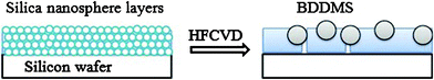 | ||
| Scheme 1 Steps in BDDMS fabrication: (1) a piece of silicon wafer was covered with layers of silica nanospheres;(2) during the HFCVD process, the BDDMS were obtained in the silica matrix. | ||
Uniform silica nanospheres were prepared by hydrolysis of tetraethyl orthosilicate (TEOS) in an alcohol medium in the presence of water and ammonia using a modified procedure, originally described by Stöber et al.7 To achieve arranged silica nanosphere layers, a piece of pretreated silicon wafer was vertically dipped into a 10 ml vessel containing 4 ml silica nanospheres (2.0 wt%) dispersed in ethanol. Following the evaporation of the ethanol, the silica nanospheres were packed in an orderly fashion under induction of the capillary force.
Diamond deposition was carried out in a conventional HFCVD reactor. An acetone solution containing 0.5% trimethyl borate was used as the carbon source. The carbon source![[thin space (1/6-em)]](https://www.rsc.org/images/entities/char_2009.gif) :H2 flow ratio was 200:50 sccm, and the growth duration was 2 h. The silicon wafer covered with the silica nanosphere layers was used as the substrate.
:H2 flow ratio was 200:50 sccm, and the growth duration was 2 h. The silicon wafer covered with the silica nanosphere layers was used as the substrate.
An SEM image of the silica nanospheres is shown in Fig. 1. As can be seen, most of the silica nanospheres, around 200 nm in diameter, were assembled in a nearly ordered array. A few defects were observed in the silica layers; these defects can hardly affect the BDDMS growth and are even likely to be ideal sites of CVD nucleation.
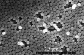 | ||
| Fig. 1 SEM image of the silica nanosphere layers on a Si wafer. | ||
After the CVD process, polycrystalline diamond microspheres were successfully formed in the silica-nanosphere-layers matrix. The shape, microstructure, and distribution of the BDDMS were determined by means of SEM and distribution analysis. Well-separated spherical particles of conductive diamond are clearly observed in Fig. 2a and 2b. From Fig. 2b and 2c, we can estimate that these spheres have diameters of around ten microns, with smooth surfaces. Observation by distribution analysis (Fig. 2e) also indicates the formation of most spherical BDDMS with a size distribution range of 8–17 μm.
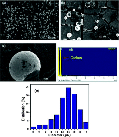 | ||
| Fig. 2 SEM images at (a) and (b) low magnification and (c) high magnification, (d) EDS analysis, and (e) histogram of size distribution of the BDDMS. | ||
It can be clearly observed that the silica matrix had transformed to a cracked and loose agglomeration, like a ‘paddy field’, after diamond deposition. And the BDDMS, like twinkling peals, were dispersed in the ‘paddy field’. It is not hard to pick out these ‘pearls’ in the ‘field’ by proper physical and chemical methods. Chemical composition analysis by energy dispersive spectroscopy (EDS) (Fig. 2d) confirms that only the carbon element of diamond is present.
The results of this experiment can therefore be summarized as follows: (i) diamond growth started from many individual nucleation sites in the silica layers and (ii) further growth from these sites was spherical without constraints (such as neighboring nodules or semispheres). The nucleation site density in the silica matrix is markedly dispersed and the morphology of the diamond crystals is observed to be substantially different from that of crystals grown directly on molybdenum and silicon wafers.
To separate the microspheres from the substrate, the BDDMS mixed with the debris of the silica matrix were removed carefully by blade from the silicon wafer and transferred to a centrifugal tube. After ultrasonic treatment in 5% HF and 5% NaOH solutions for 30 min, respectively, the by-product from silica was dissolved and removed. Then the BDDMS were separated by sedimentation in the suspension after centrifugation.
Raman spectroscopy was used to evaluate the quality of the monodisperse BDDMS. It is should be noted that the BDDMS were placed on the surface of a silicon wafer during the Raman measurements. Therefore, a sharp peak appears in the Raman spectrum at around 519 cm−1 caused by the phonon of silicon at the Brillouin zone. The Raman spectrum depicted in Fig. 3 shows a strong peak at 1332 cm−1, indicative of the sp3carbon of the BDDMS crystallite. A single, sharp peak at 1332 cm−1 in the Raman spectrum is frequently used as a signature of high crystalline quality. It has been concluded that the 1240 cm−1 is related to disorder within the diamond lattice or boron-related electronic transitions.1 From the intensity of the 1240 cm−1 peak compared with the sp3 feature (1332 cm−1) we estimated that the boron doping level is between hundreds and thousands of ppm.1 The spectrum also indicates scattering intensity from non-diamond sp2carbon impurities centered between 1550 and 1650 cm−1 with a broad and weak peak.8
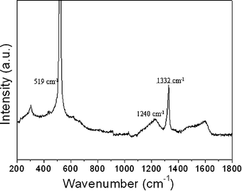 | ||
| Fig. 3 Raman spectrum of the BDDMS. | ||
In conclusion, the successful fabrication of BDDMS has opened a new route in diamond materials synthesis science. The BDDMS preparation based on a silica nanoparticle substrate and HFCVD technology can be developed into a simple protocol for the construction of a series of monodisperse and micro-sized diamond materials. The strategy outlined here may also be useful for preparing a wide range of conductive diamond particles or powders with novel electroanalytical, catalytic, and capacitive properties. As a novel style of conductive diamond material, research on its properties and potential applications is expected. Further studies on the electrocatalytic and biosensing properties of the BDDMS are now being carried out in our lab.
Acknowledgements
The authors gratefully acknowledge the financial support of the start-up science research foundation for the young teachers of Sichuan University (No. 2009SCU11012).References
- A. Fujishima, Y. Einaga, T. N. Rao and D. A. Tryk, Diamond Electrochemistry, Elsevier, Amsterdam, BKC, Tokyo, 2005 Search PubMed.
- R. Koba, Carbon, 1990, 28, 798–802 Search PubMed.
- (a) A. E. Fischer and G. M. Swain, J. Electrochem. Soc., 2005, 152, B369–B375 CrossRef CAS; (b) L.-C. L. Huang and H.-C. Chang, Langmuir, 2004, 20, 5879–5884 CrossRef CAS.
- S. Ferro, J. Mater. Chem., 2002, 12, 2843–2855 RSC.
- (a) Y. Chakk, R. Brener and A. Hoffman, Appl. Phys. Lett., 1995, 66, 2819–2821 Search PubMed; (b) A. B. Harker and J. F. DeNatale, J. Mater. Res., 1990, 5, 818–823 Search PubMed.
- W. Kulisch and C. Popov, Phys. Status Solidi A, 2006, 203, 203–219 CrossRef CAS.
- (a) W. Stöber, A. Fink and E. Bohn, J. Colloid Interface Sci., 1968, 26, 62–69 CrossRef; (b) W. P. Hsu, R. Yu and E. Matijević, J. Colloid Interface Sci., 1993, 156, 56–65 CrossRef.
- A. C. Ferrari and J. Robertson, Phys. Rev. B: Condens. Matter, 2000, 61, 14095–14107 CrossRef CAS.
| This journal is © The Royal Society of Chemistry 2011 |