Patterning cell using Si-stencil for high-throughput assay
Jinbo
Wu
a,
Mengying
Zhang
a,
Longqing
Chen
b,
Vivian
Yu
c,
Joseph
Tin-Yum Wong
c,
Xixiang
Zhang
b,
Jianhua
Qin
d and
Weijia
Wen
*a
aThe Department of Physics and KAUST-HKUST Micro/Nanofluidic Joint Laboratory, The Hong Kong University of Science and Technology, Clear Water Bay, Hong Kong. E-mail: phwen@ust.hk; Fax: 852 23581652; Tel: 852 23587979
bAdvanced Nanofabrication, Imaging and Characterization Core Lab, King Abdullah University of Science and Technology, Thuwal 23955-6900, Kingdom of Saudi Arabia
cDivision of Life Science, The Hong Kong University of Science and Technology, Clear Water Bay, Hong Kong
dDalian Institute of Chemical Physics, Chinese Academy of Sciences, 457, Zhongshan Road, 11603, China
First published on 31st August 2011
Abstract
In this communication, we report a newly developed cell pattering methodology by a silicon-based stencil, which exhibited advantages such as easy handling, reusability, hydrophilic surface and mature fabrication technologies. Cell arrays obtained by this method were used to investigate cell growth under a temperature gradient, which demonstrated the possibility of studying cell behavior in a high-throughput assay.
Most cell processes in vivo are controlled by microenvironmental stimuli, which include neighboring cells, extracellular matrices, soluble factors and physical forces.1 Complex signals such as these cannot adequately be manipulated by conventional cell-culture methods. Over the past few years however, microscale technologies have emerged as powerful tools for realizing this complexity,2 providing not only precise cell control and reagent distribution,3–5 but also a high-throughput assay.6 Therein, cell patterning has been used as an effective experimental method to create two or three-dimensional biological structures for studying cell interactions and artificial organs in vitro.7–9
Micropatterned cell structures have been achieved by means of inkjet printing,10,11 micropatterned surfaces,12–15 microfluidics,16–18 and stencils.19–22 The microfabricated stencil, in fact, is a useful and simple approach that obviates the multi-step fabrication required to produce micropatterned surfaces.23 Stencils, as noted in previous reports, can be made from stainless steel,21 Norland Optical Adhesive 73,24 PDMS,25–27 or parylene.7,19 Hard materials are seldom used, on account of the complicated fabrication processes involved and their inability to seal effectively to surfaces.19 Nonetheless, in this paper, we present a facile methodology for cell micro-patterning which employs silicon-based stencils (Si-stencils). The Si-stencil provides the advantages of an inert and hydrophilic surface, reusability, and easy handling. Moreover, well developed semiconductor techniques facilitate the microfabrication of high-resolution, reproducible Si-stencils. The cell pattern formed with our improved methodology showed that the Si-stencil offers flexibility and wide applicability, from large-scale cell patterns all the way down to the single-cell level.
Additionally, in the present study, we integrated a two-dimensional cell array patterned by the Si-stencil with a temperature gradient of 10 °C. This type of integrated device allows for multiple analyses on a single device in combinatorial fashion: different temperatures, with different cell-growth results. The cell-growth results demonstrated that the device can be used to study either cell behavior or cellular communication in high-throughput assay.
Experimental section
Si-stencils were fabricated using two common MEMS techniques: photolithography and dry etching. The process is schematized in Fig. 1a. The starting material was a double-side polished Si wafer of 400 μm thickness. The wafer was patterned with a photoresist (PR) using photolithography, and subsequently dry etched on the front side by inductively coupled plasma-deep reactive ion etching (ICP-DRIE). The same process was repeated on the back side so as to generate a hole array through the wafer prior to removal of the PR. The full wafer was then baked in a furnace in order to grow a 200 nm thermal Si oxide layer on the surface for passivation, after which, finally, it was cut into stencils. The Si-stencils, with a pattern area of 100 mm2 and with hole diameters (Dh) ranging from 8 to 400 μm, were cleaned with piranha solution (H2SO4:H2O2 = 10![[thin space (1/6-em)]](https://www.rsc.org/images/entities/char_2009.gif) :
:![[thin space (1/6-em)]](https://www.rsc.org/images/entities/char_2009.gif) 1) at 120 °C for 10 min and rinsed with DI water. Fig. 1b is a scanning electron micrograph of one of the Si-stencils. The Dh in this case is 13 μm. In the cross-section view, the microchannel is ∼70 μm in length (the thickness of the Si-stencil in the area of the hole array) and of funnel shape, with upper and lower diameters of 13.5 μm and 16.9 μm, respectively. Since the upper surface was attached to the culture dish, such a funnel shape could not affect the cell patterning, and in fact, the upper diameter (13.5 μm) is regarded as effective.
1) at 120 °C for 10 min and rinsed with DI water. Fig. 1b is a scanning electron micrograph of one of the Si-stencils. The Dh in this case is 13 μm. In the cross-section view, the microchannel is ∼70 μm in length (the thickness of the Si-stencil in the area of the hole array) and of funnel shape, with upper and lower diameters of 13.5 μm and 16.9 μm, respectively. Since the upper surface was attached to the culture dish, such a funnel shape could not affect the cell patterning, and in fact, the upper diameter (13.5 μm) is regarded as effective.
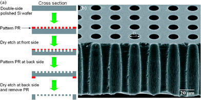 | ||
| Fig. 1 (a) A process flow diagram illustrating the fabrication procedure of the Si-stencil using two MEMS techniques. Detail description of the steps is in the text. (b) Scanning electron micrograph of a Si-stencil with 13 μm Dh. The Si-stencil was cut through the holes to reveal its cross section. | ||
We used HeLa cells to examine the Si-stencils preparatory to the cell array. The cells, derived from cervical cancer cells, were obtained from the American Type Culture Collection (ATCC; Manassas, VA, USA). They were cultured, in Minimum Essential Medium supplemented with 10% fetal bovine serum (FBS), 100 unit/mL penicillin and 100 mg mL−1streptomycin, at 37 °C in a 5%-CO2-humidified incubator. For routine culturing, cells were passaged every 1–2 days to maintain the confluency at approximately 85%. For sub-culturing, the cells were washed with pre-warmed phosphate-buffered saline (PBS) and then detached from the substrate by treatment with pre-warmed 0.25% (w/v) trypsin. When the cells were detached from the dish, fresh culture medium was added. The cell number was estimated prior to the cell culture.
The Si-stencils were each sterilized by UV light on both sides for 15 min before use. As shown in Fig. 2a, a drop of culture medium without HeLa cells was attached to the bottom of the culture dish prior to cell loading. Then, a Si-stencil was pressed onto the drop in order to fill its hole array with culture medium and, thereby, prevent air-bubble formation during cell loading. To maintain pressure sufficient to keep the stencil attached to the dish bottom, a pressed polydimethylsiloxane (PDMS; Dow Corning Corporation) frame was positioned between the stencil and the cover of the dish, and the cover was fixed to the dish by tape. After loading onto the stencil, the cells were allowed to spread and adhere to the culture dish through the holes for 5 h in an incubator. Then, the stencil was removed and the culture dish was washed twice with culture medium to remove unattached or poorly attached cells.
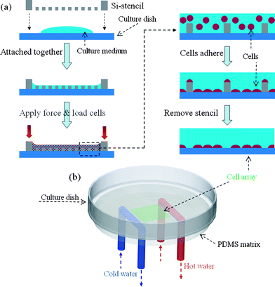 | ||
| Fig. 2 (a) Schematic illustration of patterning cell on culture dish by the Si-stencil. See text for details. For better view, the last three steps were enlarged to see the cells. (b) 3D view of the experimental setup for creation of thermal gradient (not to scale). Cold and hot water flow through the blue and red U-shaped tube, respectively. Both tubes were attached to the bottom of culture dish by the PDMS matrix. In the centre of the culture dish, there was a cell array shown in green color. | ||
Two parallel U-shaped steel tubes (inner diameter [ID] = 0.7 mm, outer diameter [OD] = 1.1 mm, hereafter U-tubes) positioned 12 mm apart were fixed in the PDMS matrix. The matrix was then attached to the backside of the culture dish (Fig. 2b, not to scale), in the centre of which was the Si-stencil-produced 10 mm × 10 mm cell pattern (shown in green color). Cold and hot water is circulated in two independent closed circuits (not shown in Fig. 2b) through the two U-tubes respectively, by means of two peristaltic pumps (EW-77120-52, C/L, Masterflex) and two reservoirs. The U-tubes permit fast heat transfer to/from the culture dish, after which hot/cold water flows back to the hot/cold water reservoirs. The water temperature in the hot water reservoir is maintained by a temperature controller (KT4, Panasonic), while that in the cold water reservoir is kept at room temperature by an air-conditioner. The temperature difference between the two U-tubes creates a thermal gradient across the culture dish.
In order to determine the quality and uniformity of the temperature gradient, an infrared (IR) camera (Thermalvision A40 M, FLIR Systems Inc.) was employed to detect both the thermal distribution and the local temperature. After the cold and hot flows were initiated, about 30 min was required to establish a steady gradient (25–35 °C). The temperature was monitored every 10 min for 2 h; the fluctuation observed was on the order of ±1 °C. Once the temperature gradient was established, the culture dish with the cell array was attached to the PDMS matrix. The entire setup was maintained in a 5%-CO2-humidified chamber. Phase-contrast images of the cell array, at four positions along L1 direction, were taken every 6 h as subject to the thermal gradient effect.
Results and discussion
As a hard material, the Si-stencil is prone to the same drawback as any metallic stencil: it does not seal well against the substrate and, therefore, cannot guarantee that a cell suspension does not spread beyond the hole area, which fact limits its application to very dilute cell suspensions.21,25 To overcome this obstacle, in the present study the Si-stencil was pressed close to the substrate (culture dish) during cell patterning. Cell-suspended media of 1×10⁵∼107cells ml−1 concentrations was used to test our methodology. Fig. 3a–d show the cell-pattern results for the 1×10⁷cells ml−1 concentration with different Dh. Even at such a high concentration, no cell was found to have spread beyond the hole area.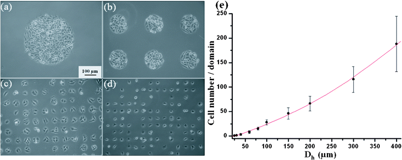 | ||
| Fig. 3 (a–d) Phase contrast microscopy image of HeLa cell patterned with different Dh: a = 400 μm, b = 150 μm, c = 40 μm, d = 30 μm, respectively. All images are at the same magnification. (e) Cell number per domain as a function of Dh. Cells were counted and averaged over 50 domains of each size. | ||
The metallic stencil has another drawback: the difficulty of fabricating metallic stencils with Dh on the order of a single cell (∼10–15 μm).25 However, thanks to the availability of well developed fabrication processes in MEMS, Si-stencil hole arrays can be fabricated easily with Dh down to 8 μm, and moreover, both thickness and Dh can be individually varied. Moreover, mature fabrication processes and the well established product line in MEMS technologies allow for the mass-producibility, low cost of the Si-stencil and even immediate commercial availability to biologists. In the present study, Si-stencils with Dh in the 8–400 μm range were fabricated to test our methodology. The above-noted Fig. 3a–d provide the cell-pattern results for Dh = 400, 150, 40, and 30 μm, respectively. Additionally, the cell number in a single domain for each Dh was counted, and the data plotted in Fig. 3e as a function of Dh. As is apparent, the Dh significantly influenced the cell number. When the Dh = 30 μm, a single-cell array could be obtained (Fig. 3d). The average percentage of single cells was as high as 60%. Such a single-cell array can be used, further, to study high-throughput cultures in single-cell-level applications including drug-induced apoptosis16,18 and cell–cell communication between individual cells.
Compared with the elastomeric stencils, the Si-stencil is rigid, and so handling for alignment and large-area patterning is both possible and easy.25,28 Conversely, it cannot, unlike elastomeric stencils, be used on a curved surface. We consider the rigidity of the Si-stencil to be a fundamental limitation.
By contrast with the hydrophobic surface of the polymer stencils,19,23,25 the Si-stencil surface (silicon dioxide) is hydrophilic. A low contact angle (about 5°) is obtainable after cleaning with piranha solution, so that the culture medium can fill stencil holes easily. This unique advantage avoids the formation of air bubbles that become trapped in the Si-stencil during cell seeding; no additional, air-bubble-removal procedure, then, is needed. In the present study, no air bubbles were found, not even in the Si-stencil with a Dh as small as 8 μm.
Two methods of used-stencil cleaning were trialled: wet cleaning by piranha solution at 120 °C for 10 min, and dry cleaning by O2 plasma treatment (IPC2000 Photo Resist Asher, Branson) for 30 min. The Si-stencils recovered by either method were then reused for cell patterning, and showed no observable variation. This reusability advantage is owed to the biocompatibility, inertness, smoothness and uniformity of silicon-dioxide-coated Si-stencil surfaces, which minimize adsorption and inhibition.29
To demonstrate the cell array has potential application in high-throughput screening, we integrated it with a temperature gradient. Fig. 4a is a thermal image of the culture dish's bottom surface taken when the thermal gradient was stable. The cell array, highlighted by the green square, is located in the centre of the image. Temperatures along L1 were measured and plotted in Fig. 4b as a function of position, which data indicate that a reasonable and uniform temperature gradient was generated in the L1 direction. The temperature difference between the two ends, over a distance of 10 mm, was about 10 °C. The cell domains were subjected to this thermal gradient.
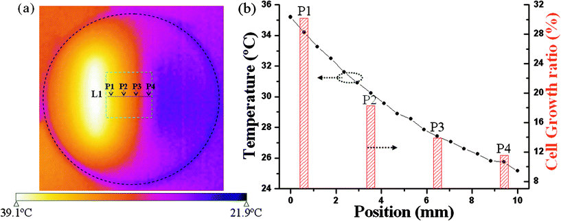 | ||
| Fig. 4 (a) Infrared thermographic image of the culture dish was taken to show the thermal gradient. L1 stands for line 1. (b) Black curve: temperature as a function of position along L1 direction; Red histogram: cell growth ratio of four places (P1, P2, P3 and P4) as a function of position along L1. | ||
To evaluate the cell growth under the temperature gradient, we measured the cell number at four positions (P1, P2, P3 and P4 as marked in Fig. 4a) along L1 and calculated, over 24 h, the cell-growth ratio (CGR):
 is the cell number in nine domains in one image (see Fig. 5) at time t0, and
  is the cell number at the same position at time t1. The results are plotted in Fig. 4b (the red histogram) as a function of their positions along L1 axis. In the histogram and the L1 curve, the CGR seems to present the same trend as the temperature gradient: a decline as the position moves. Fig. 5 shows phase-contrast images of the cell array at two of fours positions: at 26 °C (P4, a–d), and 34 °C (P1, e–h). The temperatures were estimated according to their positions in the L1 curve and the images were captured 0, 6, 18, and 24 h after the thermal gradient was applied. In Fig. 5, the effect of the gradient on cell growth after 24 h is clear: the cell domains are still isolated from each other at the lower temperature, whereas at the higher temperature, they begin to connect viacell bridges. Although we observed the CGR at only four positions (or temperatures) over 24 h, our result confirms that the thermal gradient made an effective impact on the cell growth and, furthermore, that our integrated device is suitable for long-term cell cultures. Additionally, since the cell-free region can be considered as a wound, a cell pattern could be used to mimic wound healingin vitro. Wound-healing assays could be high-throughput screened at different temperatures in one culture dish.
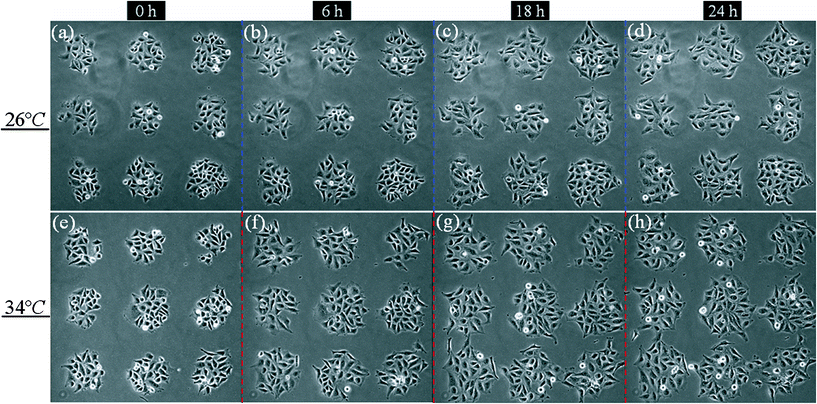 | ||
| Fig. 5 Cell growth under thermal gradient. (a–d) at the same location of 26 °C; (e–h) at the same location of 34 °C. They are captured in the time of 0, 6, 18, and 24 h after applied thermal gradient. | ||
Conclusions
In summary, we successfully developed a convenient, efficient cell-patterning methodology using a Si-stencil with wide potential applications. The Si-stencil offers the advantages of easy handling, mature fabrication technologies, and hydrophilic surface and could be recovered by either a dry or wet cleaning method. Si-stencils with Dh in the 8–400 μm range were fabricated and tested with HeLa cells. Cell pattern results indicated that the Si-stencil can be used from large-scale to single-cell manipulation. Furthermore, a cell array obtained by the Si-stencil was used to investigate cell growth under temperature gradient. Our results guarantees further applications in tissue engineering, biosensors and high-throughput screening. One such application is a high-throughput cell-based assay, which has attracted great interest for its reduction of screening costs incurred in the drug discovery process.30Acknowledgements
This work is supported by Hong Kong RGC grant HKUST 604710 and research grant RPC10SC01, respectively.References
- S. R. Khetani and S. N. Bhatia, Nat. Biotechnol., 2008, 26, 120–126 CrossRef CAS.
- C. J. Bettinger and J. T. Borenstein, Soft Matter, 2010, 6, 4999–5015 RSC.
- A. Khademhosseini, R. Langer, J. Borenstein and J. P. Vacanti, Proc. Natl. Acad. Sci. U. S. A., 2006, 103, 2480–2487 CrossRef CAS.
- P. Domachuk, K. Tsioris, F. G. Omenetto and D. L. Kaplan, Adv. Mater., 2010, 22, 249–260 CrossRef CAS.
- S. Y. Yoo, W. -J. Chung, T. H. Kim, M. Le and S. -W. Lee, Soft Matter, 2011, 7, 363–368 RSC.
- S. Sugiura, J. -i. Edahiro, K. Kikuchi, K. Sumaru and T. Kanamori, Biotechnol. Bioeng., 2008, 100, 1156–1165 CrossRef CAS.
- D. Wright, B. Rajalingam, S. Selvarasah, M. R. Dokmeci and A. Khademhosseini, Lab Chip, 2007, 7, 1272–1279 RSC.
- M. A. Cole, N. H. Voelcker, H. Thissen and H. J. Griesser, Biomaterials, 2009, 30, 1827–1850 CrossRef CAS.
- A. Offenhäusser, S. Böcker-Meffert, T. Decker, R. Helpenstein, P. Gasteier, J. Groll, M. Möller, A. Reska, S. Schäfer, P. Schulte and A. Vogt-Eisele, Soft Matter, 2007, 3, 290–298 RSC.
- M. Nakamura, A. Kobayashi, F. Takagi, A. Watanabe, Y. Hiruma, K. Ohuchi, Y. Iwasaki, M. Horie, I. Morita and S. Takatani, Tissue Eng., 2005, 11, 1658–1666 CrossRef CAS.
- P. Calvert, Science, 2007, 318, 208–209 CrossRef CAS.
- L. H. Jin, B. Y. Yang, L. Zhang, P. L. Lin, C. Cui and J. Tang, Langmuir, 2009, 25, 5380–5383 CrossRef CAS.
- K. Y. Suh, J. Seong, A. Khademhosseini, P. E. Laibinis and R. Langer, Biomaterials, 2004, 25, 557–563 CrossRef CAS.
- Y. Tsuda, A. Kikuchi, M. Yamato, A. Nakao, Y. Sakurai, M. Umezu and T. Okano, Biomaterials, 2005, 26, 1885–1893 CrossRef CAS.
- C. D. McFarland, C. H. Thomas, C. DeFilippis, J. G. Steele and K. E. Healy, J. Biomed. Mater. Res., 2000, 49, 200–210 CrossRef CAS.
- D. Wlodkowic, S. Faley, M. Zagnoni, J. P. Wikswo and J. M. Cooper, Anal. Chem., 2009, 81, 5517–5523 CrossRef CAS.
- I. Inoue, Y. Wakamoto, H. Moriguchi, K. Okano and K. Yasuda, Lab Chip, 2001, 1, 50–55 RSC.
- D. D. Carlo, L. Y. Wu and L. P. Lee, Lab Chip, 2006, 6, 1445–1449 RSC.
- D. Wright, B. Rajalingam, J. M. Karp, S. Selvarasah, Y. Ling, J. Yeh, R. Langer, M. R. Dokmeci and A. Khademhosseini, J. Biomed. Mater. Res., Part A, 2008, 85, 530–538 CrossRef.
- C. H. Cho, J. Park, A. W. Tilles, F. Berthiaume, M. Toner and M. L. Yarmush, BioTechniques, 2010, 48, 47–52 CrossRef CAS.
- Y. Jimbo, H. P. C. Robinson and A. Kawana, IEEE Trans. Biomed. Eng., 1993, 40, 804–810 CrossRef CAS.
- K. Atsuta, H. Noji and S. Takeuchi, Lab Chip, 2004, 4, 333–336 RSC.
- E. Ostuni, R. Kane, C. S. Chen, D. E. Ingber and G. M. Whitesides, Langmuir, 2000, 16, 7811–7819 CrossRef CAS.
- Y. Zheng, W. Dai, D. Ryan and H. Wu, Biomicrofluidics, 2010, 4, 036504 CrossRef.
- A. Folch, B. -. Jo, O. Hurtado, D. J. Beebe and M. Toner, J. Biomed. Mater. Res., 2000, 52, 346–353 CrossRef CAS.
- C. -H. Hsieh, C. -J. C. Huang and Y. -Y. Huang, Biomed. Microdevices, 2010, 12, 897–905 CrossRef CAS.
- N. A. Raof, W. K. Raja, J. Castracane and Y. Xie, Biomaterials, 2011, 32, 4130–4139 CrossRef.
- M. Yamato, C. Konno, M. Utsumi, A. Kikuchi and T. Okano, Biomaterials, 2002, 23, 561–567 CrossRef CAS.
- M. A. Shoffner, J. Cheng, G. E. Hvichia, L. J. Kricka and P. Wilding, Nucleic Acids Res., 1996, 24, 375–379 CrossRef CAS.
- M. -Y. Lee and J. S. Dordick, Curr. Opin. Biotechnol., 2006, 17, 619–627 CrossRef CAS.
| This journal is © The Royal Society of Chemistry 2011 |

