Orthogonal processing: A new strategy for organic electronics†
Alexander A.
Zakhidov
a,
Jin-Kyun
Lee
ab,
John A.
DeFranco
ac,
Hon Hang
Fong
ad,
Priscilla G.
Taylor
a,
Margarita
Chatzichristidi
e,
Christopher K.
Ober
a and
George G.
Malliaras
a
aDepartment of Materials Science and Engineering, Cornell University, Ithaca, NY 14853, USA. E-mail: cko3@cornell.edu; Fax: +1 607 255 2365; Tel: +1 607 255 8417
bDepartment of Polymer Science and Engineering, Inha University, Incheon, 402-751, South Korea
cOrthogonal Inc., Ithaca, NY 14850, USA
dSchool of Electronic, Information and Electrical Engineering, National Engineering Lab of TFT-LCD Materials and Technologies, Shanghai Jiao Tong University, Shanghai, 200240, P.R. China
eChemistry Department, University of Athens, Zografou, 15771, Greece
First published on 7th April 2011
Abstract
The concept of chemical orthogonality has long been practiced in the field of inorganic semiconductor fabrication, where it is necessary to deposit and remove a layer of photoresist without damaging the underlying layers. However, these processes involving light sensitive polymers often damage organic materials, preventing the use of photolithography to pattern organic electronic devices. In this article we show that new photoresist materials that are orthogonal to organics allow the fabrication of complex devices, such as hybrid organic/inorganic circuitry and full-colour organic displays. The examples demonstrate that properly designed photoresists enable the fabrication of organic electronic devices using existing infrastructure.
Introduction
The two extremes of miscibility and orthogonality play a central role in the fabrication of inorganic semiconductor devices. Miscibility allows the removal of layers (by dissolution) when or where they are no longer needed: The wet-etching of various materials with suitable solvents is an example of processes requiring miscibility between the etchant and the target material. Orthogonality, on the other hand, is necessary when a layer deposited from solution must not damage underlying layers. This is the case during the deposition or removal of a photoresist film: The integrity of underlying inorganic electronic materials is not at risk during this process, as their “hard” nature renders them insoluble to the solvents used during photolithographic processing. Leveraging these relationships between materials, silicon electronics has enjoyed great success in scaling devices to smaller and smaller dimensions.When considered within the context of organic electronics, however, the condition of orthogonality between photoresists and electronic materials is not met.1,2 Organic electronic materials are sensitive to the solvents used for the deposition of a photoresist, as well as to the aqueous alkaline solutions used for its development. As a result, alternative strategies have been applied to the patterning of organics,3 including direct deposition-patterning methods (e.g. inkjet printing,4 shadow mask deposition, organic vapour jet printing,5 screen printing6 and micro-contact printing7), the use of protective interlayers between electronic materials and photoresist films,8–10 and modifications of the organic semiconductors themselves to render them stable under standard photolithographic conditions.11,12 The first two strategies require the use of new equipment or increase the complexity of processing. They also limit the range of materials compatible with a particular process (e.g. specially formulated inks for printing or organic semiconductors compatible with traditional photoresists and developers).13,14 The last strategy depends heavily on the synthesis of speciality materials, which often do not match the performance of state-of-the-art organics.
What has not yet been widely considered is a change in the fundamental chemistry of the photoresist materials themselves. We recently took advantage of the fact that the vast majority of organic materials are either oleophilic or hydrophilic and are hence orthogonal to highly fluorinated chemicals (Fig. 1a and 1b).15 Therefore, appropriate fluorinated photoresists, such as the molecule shown in Fig. 1c, can be used to pattern organic layers.16 The availability of such orthogonal photoresists promises to enable the fabrication of complex device structures, expanding the range of possibilities for organic electronics. In this letter, we report a few examples of such device structures, including micro- and nanoscale organic thin film transistors (OTFTs) with top contacts, hybrid organic/inorganic integrated circuits, and full colour displays based on organic light-emitting diodes (OLEDs).
![(a) Schematic representation of three classes of mutually orthogonal materials. (b) Photograph of three phase-separated solutions, which represent each class: bottom – a semi-perfluoroalkyl polyfluorene in a hydrofluoroether (HFE 7500), middle – ruthenium(ii) tris(bipyridine) with tetrafluoroborate counter ions {[Ru(bpy)3]2+(BF4−)2} in water, top –poly(9,9′-dioctylfluorene-co-benzothiadiazole) (F8BT) in 1-octadecene. (c) A resorcinarene-based fluorinated photoresist used in this work.](/image/article/2011/SC/c0sc00612b/c0sc00612b-f1.gif) | ||
| Fig. 1 (a) Schematic representation of three classes of mutually orthogonal materials. (b) Photograph of three phase-separated solutions, which represent each class: bottom – a semi-perfluoroalkyl polyfluorene in a hydrofluoroether (HFE 7500), middle – ruthenium(II) tris(bipyridine) with tetrafluoroborate counter ions {[Ru(bpy)3]2+(BF4−)2} in water, top –poly(9,9′-dioctylfluorene-co-benzothiadiazole) (F8BT) in 1-octadecene. (c) A resorcinarene-based fluorinated photoresist used in this work. | ||
Results and discussion
As a first target, we fabricated top-contact OTFTs having channel lengths which are difficult to achieve with conventional methods. In general, top contact transistors are made by vacuum deposition of source and drain contacts through a stencil. This method, however, does not typically provide channel lengths smaller than tens of micrometres. To prove that photolithography can yield top contact OTFTs, we used an orthogonal photoresist based on the semi-perfluoroalkyl resorcinarene (Fig. 1c).16 This imaging material has proven to have high resolution patterning capabilities, down to 0.4 μm lines with 365 nm UV exposure and down to 30 nm with e-beam exposure.16 It also exhibits straight or slightly undercut sidewalls, which are essential to perform patterning by lift-off (Fig. 2a). We successfully fabricated top contact transistors with 1 μm channel lengths using pentacene under 365 nm UV exposure conditions, as shown in Fig. 2b. Pentacene film growth is known to be particularly sensitive to substrate roughness, which makes top contact devices show superior performance in comparison to bottom contact ones.17 The field effect mobility of the photolithographically fabricated pentacene transistor was found to be 0.45 cm2V−1s−1. This is essentially the same field-effect mobility (but at a smaller channel length) as those in transistors made by vacuum deposition of metal through a stencil (Fig. 2c, and also Supplementary Information S1†), indicating that the process does not damage the delicate pentacene films.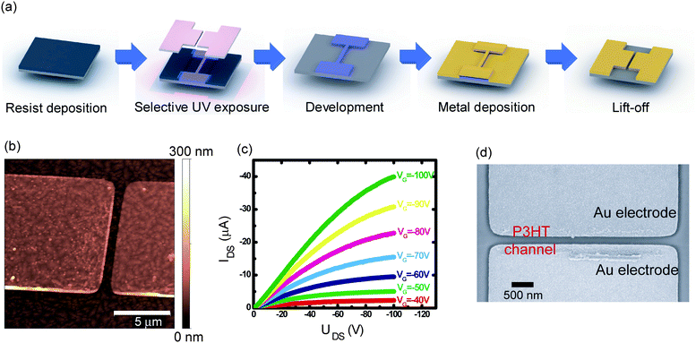 | ||
| Fig. 2 (a) The lift-off process used to pattern transistors with 1 μm channel length on top of a pentacene film. (b) AFM image, and, (c) output characteristics of one of these transistors. (d) Scanning electron micrograph of a P3HT transistor with a channel length of 200 nm. | ||
The channel length was limited in this case only by capabilities of the imaging tool and not by the properties of the photoresist itself. Fig. 2d shows a top contact OTFT with a channel length of 200 nm using poly(3-hexylthiophene) (P3HT) as the semiconductor. The performance of these transistors was found to be contact limited (Supplementary Information S2†) due to the small channel length, but the data show that lithography can achieve organic device geometries that are difficult to obtain using other fabrication techniques. It should be noted that a relevant idea was recently employed by Dhar et al., who used fluorinated sacrificial layers (which were subsequently removed with highly fluorinated solvents) as contact masks.18 The use of fluorinated resists allows us to extend the pattering of organics towards the fabrication of more complex structures, such as hybrid organic/inorganic integrated circuitry and full colour organic-based displays.
In order to prove the process at a higher level vertical integration, we fabricated ring oscillators based on 1 μm channel length pentacene OTFTs (Fig. 3a). The device consists of several layers patterned with five subsequent photolithographic steps: The first three layers were the gate electrode (Au), the gate dielectric (Al2O3), and the interconnect lines (Cr/Au), and were patterned using a commercially available DNQ-novolac resist. The third and fourth layers were the semiconductor (pentacene) and source–drain contacts (Au), and were patterned using the resorcinarene resist. Fabrication details can be found in the Experimental section. The devices exhibited a turn-on voltage of 10–15 V and had a peak frequency of 18 kHz at 55 V of applied bias. The gate delay of the five-stage ring oscillator was 5.5 μs. This performance compares favourably to OTFT-based ring oscillators made with other methods.19 It should be noted that the devices were fairly reproducible under a lab environment, with >90% of tested oscillators functioning properly. This example demonstrates that organic materials can be patterned using the same tools as inorganic ones, which is very attractive for the fabrication of hybrid circuitry.
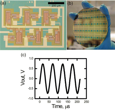 | ||
| Fig. 3 (a) Optical micrograph of a ring oscillator based on top contact pentacene OTFTs with 1 μm channel length. (b) Picture of multiple ring oscillators on a 4-inch wafer. (c) Output characteristics of the device at VDD = −55 V. | ||
A second example, which highlights lateral integration, is the fabrication of a full colour OLED display, in which three semiconducting polymers were patterned next to each other without damaging one another (Fig. 4c). Three different light-emitting polymers (LEP) from the polyfluorene family were used and the individual pixel structure was Indium-Tin-Oxide (ITO)/hole-injection layer (HIL)/LEP/CsF/Al. The display was realized via consecutive patterning steps for each polymer, with the fourth step for the patterning of the cathode on top of all three light-emitting polymers. We successfully fabricated arrays of light emitting pixels of 20 × 20 μm2. Larger pixels were also fabricated and were shown to have similar performance compared to reference pixels fabricated by cathode deposition through a stencil (see Supplementary Information S3†).
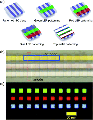 | ||
| Fig. 4 (a) The patterning sequence used for the fabrication of the display. (b) The resulting optical micrograph. (c) Electroluminescence image. | ||
Conclusions
The three examples of test-bed structures shown above demonstrate that photolithography can be applied to the fabrication of fairly complex organic electronic and hybrid devices. Hurdles still remain, such as refining the composition of the photoresists and of the processes in order to improve the pattern fidelity and to minimize the impact of processing on the properties of the organic semiconductors. These examples, however, demonstrate the importance of orthogonal photoresists for organic electronics, and show that photolithography has the potential to bring organic electronics closer to commercialisation, by leveraging existing infrastructure and expertise.Experimental section
Materials
Hydrofluoroethers (HFE 7500, HFE 7200 and HFE 7100) were donated by 3M USA and used as received. PEDOT:PSS (AI 4083) was purchased from H. C. Starck and used as received. Pentacene was purchased from Kintec and used as received. P3HT with regioregularity >99% was obtained from Plextronics and used without further purification. Light-emitting polymers, poly(9,9-dioctylfluorene) (F8) and poly[(9,9-dioctylfluorene)-co-(benzothiadiazole)] (F8BT), were purchased from American Dye Source and used as received. Ethanol, toluene, 1-octadecene were purchased from Sigma-Aldrich and used as received. Red light-emitting polymer, a statistical copolymer composed of 9,9-didodecylfluorene and 4,7-di(thiophen-2-yl)benzo[1,2,5]thiadiazole (F12TBT) (mole ratio of F12 to TBT is 4 to 1) was synthesized following a literature protocol.20Top-contact pentacene OTFTs
Highly-doped Si wafers with a thermally-grown 360 nm SiO2 layer were used as substrates. They were cleaned in isopropanol and acetone and treated with hexamethyldisilazane (HMDS). Pentacene films were deposited onto these substrates at a rate of 0.1 Å s−1 and a pressure of 5 × 10⁻⁷ Torr. 200 Å thick films were deposited, as determined by a quartz crystal monitor. Resist solutions were prepared by mixing RF-Calix-tBoc powder (15 wt%) with HFE 7500, using a small amount of propylene glycol methyl ether acetate (PGMEA) as a co-solvent. A photoacid generator (PAG, N-nonafluorobutanesulfonyloxy-1,8-naphthalimide, 0.5 wt%) was mixed into the solution and the solution was filtered through a syringe filter (nylon, 0.20 μm). After deposition of pentacene, the wafer was removed from the glove box, where a resorcinarene resist solution was spin-coated onto the wafer at 1000 rpm. Patterns were then exposed on a GCA Autostep (λ = 365 nm) exposure tool. The film went through post-exposure bake at 70 °C for 30 s and was developed in HFE 7200. After development, a layer of 50 nm thick Au film was deposited to form the source and drain contacts. Finally, the resist film was lifted off in ethanol (5 vol%)-HFE 7100 (95 vol%) mixture to leave patterned Au electrodes on top of the pentacene film.Top contact P3HT TFTviaelectron-beam patterning
A 30 nm thick film of P3HT was formed on a highly-doped Si wafer with a thermally-grown 360 nm SiO2 layer by spin-coating of the P3HT solution (1 wt% in 1,2,4-trichlorobenzene) at 3000 rpm. The film was then annealed at 100 °C for 1 h under N2 atmosphere. 200 nm Thick film of the RF-Calix-tBoc resist was formed viaspin-coating in air. The resist was exposed with a Leica VB-6HR 100 kV e-beam writer (dose 215 μC cm−2, current 1 nA). After development of the resist images in HFE 7200 for 20 s, a layer of 50 nm thick Au film was deposited on top of the P3HT film to form the source and drain contacts. Finally, the resist was lifted off in ethanol (5 vol%)-HFE 7100 (95 vol%) mixture to leave patterned Au electrodes on top of the P3HT film.Ring oscillator fabrication
Ring oscillators were fabricated in order to demonstrate multi-layer patterning using photolithography. The devices are composed of four separately patterned layers. The first two layers are gate metal and gate dielectric layers which were patterned using standard diazonaphthoquinone (DNQ)-Novalak resists. Both the pentacene layer and the source/drain electrodes were patterned using the RF-Calix-tBoc resist and fluorous developers. In order to make a surface as smooth as possible for the pentacene deposition step, a mercaptosilane monolayer was used as the adhesion layer for the Au gate electrodes. The method has been used by Mahapatro et al. to make nearly atomically flat Au films for molecular electronics applications.21 We were able to achieve Au surfaces with an RMS roughness of 6–7 Å. First, a test grade Si wafer was oxidized to form a 500 nm thick passivation layer of SiO2. The wafer was cleaned in a hot piranha solution. It was then exposed to O2 plasma for 10 min and dipped in HCl and deionised water for ten minutes. Immediately after this cleaning and surface preparation procedure, the wafer was placed in a molecular vapour deposition tool (MVD 100) where it was coated with a monolayer of 3-mercaptopropyl trimethoxysilane (MPTMS). After the monolayer was in place, a 50 nm thick Au layer was deposited onto the substrate at a rate of 0.5 Å s−1 using e-beam deposition at a pressure of 1 × 10⁻⁶ Torr. The films were measured on a Digital Instruments AFM to determine surface roughness. The gate electrode patterns were formed using a wet etch (KI/I2) using SPR220 3.0 resist image as an etch mask. A conformal coating of Al2O3 was deposited using atomic layer deposition (ALD) on an Oxford ALD tool. ALD uses self-terminating surface reactions to deposit a single monolayer at a time. The depositions took place at 110 °C using a thermal process. A 60 nm thick film of Al2O3 was deposited on top of the gate electrodes. Patterning the dielectric layer was also accomplished using a wet etch process, with the same tools as the gate electrode layer. Aluminium etchant type A (phosphoric acid, nitric acid, acetic acid) was used to etch the dielectric layer. Cr/Au interconnect lines were prepared by lift off technique, using commercial negative resist AZ NLOF 2020. Pentacene was deposited onto that substrate at a rate of 0.1 Å s−1 and a pressure of 5 × 10⁻⁷ Torr. A 20 nm thick layer was deposited, as determined by a quartz crystal monitor. A resist solution was prepared by mixing RF-Calix-tBoc powder (10 wt%) with HFE 7500, using a small amount of PGMEA as a co-solvent. A photoacid generator (N-nonafluorobutanesulfonyloxy-1,8-naphthalimide, 0.5 wt%) was mixed into the solution and the solution was filtered through a syringe filter (Nylon, 0.45 μm). After deposition of a pentacene layer, the wafer was removed from the glove box, where the resist film was spin-coated onto the wafer at 2000 rpm, forming a 300 nm thick resist film. Patterns were exposed on a GCA Autostep. The film went through a post-exposure bake at 70 °C for 30 s and was developed in HFE 7200. The uncovered areas of pentacene were etched in oxygen plasma for 30 s and the resist layer was washed away with ethanol (5 vol%)-HFE 7100 (95 vol%) mixture. Source/drain electrodes were then patterned using a lift-off method described above. After development of the RF-Calix-tBoc resist, a layer of 50 nm thick Au film was deposited on top of the pentacene to form the contacts.Passive matrix OLED display fabrication
Patterned ITO glass substrates were cleaned by non-ionic detergent and DI water, followed by 10 min UV ozone treatment (Jelight). A 40 nm thick film of PEDOT:PSS (Clevios AI 4083, H.C. Stark) was spin-coated at 3000 rpm onto the ITO substrate and baked at 180 °C for 40 min in air. A 100 nm thick film of the green light-emitting polymer, F8BT, was spin-coated onto the PEDOT:PSS film at 1000 rpm from a concentration of 15 mg cm−3 in anhydrous p-xylene, and further baked at 130 °C for 15 min under a N2 atmosphere. Then, a layer of the RF-Calix-tBoc resist was spin-coated onto the F8BT/PEDOT:PSS film. The resist film was exposed through a photo mask and developed in HFE-7200, and the resist image was then transferred onto the F8BT/PEDOT:PSS film via O2-plasma etch. The same procedure was repeated to pattern red (F12TBT) and blue (F8) pixels. Then the remaining resist film was then washed away in a hexamethyldisilazane (HMDS) (5 vol%)-HFE-7100 (95 vol%) mixture. Then another layer of the RF-Calix-tBoc resist was spin-coated on the obtained structure and a lift-off patterning of CsF (1 nm)/Al (40 nm) cathode was performed to complete the device structure.Acknowledgements
This work was supported by the NSF (DMR-0908994) and was carried out at the Cornell NanoScale Facility. The authors thank Michael Kane of the Sarnoff Corporation for the design of the ring oscillator.Conflict-of-interest statement: The authors are named as co-inventors on patents related to photolithographic patterning of organics. JAD is currently working for Orthogonal, a company that seeks to commercialize photoresists for the patterning of organics and in which CKO and GGM own shares.
Notes and references
- G. G. Malliaras and R. H. Friend, Phys. Today, 2005, 58, 53–58 CAS.
- S. R. Forrest, Nature, 2004, 428, 911–918 CrossRef CAS.
- E. Menard, M. A. Meitl, Y. Sun, J.-U. Park, D. J.-L. Shir, Y.-S. Nam, S. Jeon and J. A. Rogers, Chem. Rev., 2007, 107, 1117–1160 CrossRef CAS.
- H. Sirringhaus, T. Kawase, R. H. Friend, T. Shimoda, M. Inbasekaran, W. Wu and E. P. Woo, Science, 2000, 290, 2123–2126 CrossRef CAS.
- M. Shtein, P. Peumans, J. B. Benziger and S. R. Forrest, Adv. Mater., 2004, 16, 1615–1620 CrossRef CAS.
- Z. N. Bao, Y. Feng, A. Dodabalapur, V. R. Raju and A. J. Lovinger, Chem. Mater., 1997, 9, 1299–1301 CrossRef CAS.
- A. Kumar and G. M. Whitesides, Appl. Phys. Lett., 1993, 63, 2002–2004 CrossRef.
- P. F. Tian, P. E. Burrows and S. R. Forrest, Appl. Phys. Lett., 1997, 71, 3197–3199 CrossRef CAS.
- I. Kymissis, C. D. Dimitrakopoulos and S. Purushothaman, J. Vac. Sci. Technol., B, 2002, 20, 956–959 CrossRef CAS.
- J. D. DeFranco, B. S. Schmidt, M. Lipson and G. G. Malliaras, Org. Electron., 2006, 7, 22–28 CrossRef CAS.
- C. D. Müller, A. Falcou, N. Reckefuss, M. Rojahn, V. Wiederhirn, P. Rudati, H. Frohne, O. Nuyken, H. Becker and K. Meerholz, Nature, 2003, 421, 829–833 CrossRef.
- A. Afzali, C. D. Dimitrakopoulos and T. O. Graham, Adv. Mater., 2003, 15, 2066–2069 CrossRef CAS.
- C. Balocco, L. A. Majewski and A. M. Song, Org. Electron., 2006, 7, 500–507 CrossRef CAS.
- J. Huang, R. Xia, Y. Kim, X. Wang, J. Dane, O. Hofmann, A. Mosley, A. J. de Mello, J. C. de Mello and D. D. C. Bradley, J. Mater. Chem., 2007, 17, 1043–1049 RSC.
- Al.A. Zakhidov, J.-K. Lee, H. H. Fong, J. A. DeFranco, M. Chatzichristidi, P. G. Taylor, C. K. Ober and G. G. Malliaras, Adv. Mater., 2008, 20, 3481–3484 CrossRef CAS.
- J.-K. Lee, M. Chatzichristidi, Al.A. Zakhidov, P. G. Taylor, J. A. DeFranco, H. S. Hwang, H. H. Fong, A. B. Holmes, G. G. Malliaras and C. K. Ober, J. Am. Chem. Soc., 2008, 130, 11564–11565 CrossRef CAS.
- C. D. Dimitrakopoulos and P. R. L. Malenfant, Adv. Mater., 2002, 14, 99–117 CrossRef CAS.
- B. M. Dhar, G. S. Kini, G. Xia, B. J. Jung, N. Markovic and H. E. Katz, Proc. Natl. Acad. Sci. U. S. A., 2010, 107, 3972–3976 CrossRef CAS.
- H. Klauk, U. Zschieschang and M. Halik, J. Appl. Phys., 2007, 102, 074514 CrossRef.
- Q. Hou, Y. S. Xu, W. Yang, M. Yuan, J. B. Peng and Y. Cao, J. Mater. Chem., 2002, 12, 2887–2892 RSC.
- A. K. Mahapatro, A. Scott, A. Manning and D. B. Janes, Appl. Phys. Lett., 2006, 88, 151917 CrossRef.
Footnote |
| † Electronic supplementary information (ESI) available: Figures S1–S3. See DOI: 10.1039/c0sc00612b |
| This journal is © The Royal Society of Chemistry 2011 |