Simple, robust molecular self-assembly on germanium†
J. Nathan
Hohman
ab,
Moonhee
Kim
ab,
Heidi R.
Bednar
a,
Jeffrey A.
Lawrence
c,
Patrick D.
McClanahan
d and
Paul S.
Weiss
*abde
aCalifornia NanoSystems Institute and Department of Chemistry and Biochemistry, University of California, Los Angeles, Los Angeles, CA 90095, USA. E-mail: psw@cnsi.ucla.edu
bDepartment of Chemistry, The Pennsylvania State University, University Park, PA 16802, USA
cDepartment of Engineering Science & Mechanics, The Pennsylvania State University, University Park, PA 16802, USA
dDepartment of Physics, The Pennsylvania State University, University Park, PA 16802, USA
eDepartment of Materials Science and Engineering, University of California, Los Angeles, Los Angeles, CA 90095, USA
First published on 5th May 2011
Abstract
We report the facile fabrication of high-quality, robust alkanethiolate self-assembled monolayers (SAMs) on germanium substrates. Our approach to produce SAMs on technologically important substrates takes advantage of the many strategies previously developed for gold-thiol self-assembly. Direct self-assembly of alkanethiols on germanium is impeded by the presence of the native germanium oxide. Using a mixture of water and ethanol, we create an environment where both adsorbate and oxide are sufficiently soluble to enable SAM deposition in a single step. By manipulating reaction conditions, monolayers form spontaneously on untreated germanium, which opens new avenues for the exploitation of self-assembly on semiconductor surfaces. While our analyses initially focused on 1-dodecanethiol on Ge(100), this method is robust and we have extended its use to include a range of adsorbates on Ge(100) as well as to the Ge(111) and Ge(110) substrates.
Introduction
Self-assembled monolayers (SAMs) on Au{111} have been the model system for self-assembly for nearly 30 years; they form spontaneously, are well-ordered, and are amenable to a wide range of analyses and applications.1–6Self-assembly on Au is effective for several key reasons: the ease with which the Au{111} surface may be prepared, the instability of the gold oxide, the ability of thiols to displace contaminants during the formation of the SAM, post-adsorption molecular mobility and exchange that enable high levels of molecular-scale order, and the availability of a myriad of thiol-based adsorbates.6–18Self-assembly is also becoming increasingly relevant for soft- and hybrid-lithographic patterning on surfaces.19–30Substrates including noble metals,31–37 semiconductors,38–61 insulators, base metals, and alloys62–67 have all been employed as substrates for SAMs.6 Each system is distinct, with different surface preparation and fabrication procedures that must be employed; nanoscale order varies. Tenacious oxides on many substrates complicate the self-assembly process; removing the oxide and keeping it from reforming can add multiple fabrication steps with the potential for degradation of the atomic-scale flatness of the substrate.68
Germanium was the first semiconductor used for transistors,69 but its poorly passivating, thermally unstable, and water-soluble oxide has limited its use.70–75 High charge carrier mobilities in germanium, however, have driven recent interest in its surface chemistry and passivation.76–78 Direct alkylation of the germanium surface viaGrignard reaction was first reported in the 1960's,79–81 later followed by investigations into hydrogen,71halogen,82,83 and sulfide passivation.84–88 The tendency for such passivation layers to retard the reformation of the oxide was exploited by using alkanethiols to displace the passivation layer and to form covalent Ge–S bonds,42,89–93 opening the door for thiol-based self-assembly akin to that on gold substrates. Most recently, microscopic studies of alkanethiol92,94 and alkyl disulfide95 adsorption in vacuum have revealed insight into the binding and mechanisms of SAM adsorption on Ge and the use of monolayers on germanium nanowires and related materials.96
Here, we present a facile, robust method of molecular self-assembly on germanium. Contact angle goniometry and X-ray photoelectron spectroscopy (XPS) are used to show that SAMs may be deposited directly on the germanium surface in a single step, from a 0.5 mM solution of an alkanethiol in a 1![[thin space (1/6-em)]](https://www.rsc.org/images/entities/char_2009.gif) :1 mixture of water and ethanol. No pretreatment of the wafer is required (the germanium etch is in situ), nor is a discrete passivation step. We have thus simplified the deposition chemistry, and effectively mimicked the advantages of gold/thiol self-assembly on germanium. We focused our initial studies on SAMs formed from 1-dodecanethiol (C12) on Ge(100), but extended this methodology to a variety of other molecular systems and low index Ge surfaces. We show that the monolayers produced in this manner are as robust as those prepared by other methods.90 Lastly, our investigations of the temperature dependence of coverage supports a previously described mechanism for the formation of SAMs on germanium.92
:1 mixture of water and ethanol. No pretreatment of the wafer is required (the germanium etch is in situ), nor is a discrete passivation step. We have thus simplified the deposition chemistry, and effectively mimicked the advantages of gold/thiol self-assembly on germanium. We focused our initial studies on SAMs formed from 1-dodecanethiol (C12) on Ge(100), but extended this methodology to a variety of other molecular systems and low index Ge surfaces. We show that the monolayers produced in this manner are as robust as those prepared by other methods.90 Lastly, our investigations of the temperature dependence of coverage supports a previously described mechanism for the formation of SAMs on germanium.92
Experimental
Materials
Single-side polished, undoped Ge(100) (<40 Ω·cm resistivity, 350–400 μm thickness) and Ge(111) (<40 Ω·cm resistivity, 500–550 μm thickness) wafers were acquired from Silicon Quest International (Santa Clara, CA). Ge(110) wafers (<40 Ω·cm resistivity, 350–400 μm thickness) were acquired from Nova Electronic Materials (Flower Mound, TX). All chemicals were used as received from Sigma Aldrich (St. Louis, MO). Deionized water at 18.2 MΩ·cm resistivity was delivered by a Milli-Q system from Millipore (Billerica, MA). Glass vials (typically v-vials, part number W986259NG) were purchased from Wheaton Science Products (Millville, NJ).Fabrication of monolayers
Solutions are prepared in two steps. A 1 mM ethanolic solution of the desired alkanethiol molecule, typically C12, is prepared, which is then diluted at a 1:1 ratio with 18.2 MΩ water by volume, resulting in a 0.5 mM solution in 1:1 water–ethanol. For experiments that vary the water concentration, a measured mass of the required chemical is dissolved in ethanol, which is then diluted by 18.2 MΩ water to the appropriate volume and concentration. Adding adsorbates directly to a previously prepared water–ethanol mixture is not advised; the result is often a cloudy suspension. Though monolayers can be prepared at the same level of quality from a cloudy suspension, the resulting uncertainty in concentration is an unnecessary variable that may be controlled simply. The well-known negative excess volume characteristic of water–ethanol mixtures is ignored.97
A diamond-tipped scribe was used to cleave the germanium wafers along their structural crystallographic planes into fragments of usable size. Freshly cleaved germanium fragments are otherwise used as received. Samples are placed directly in a vial containing the water–ethanol/thiol solution, which is sealed by a Teflon insert in a plastic cap. Samples are kept at the desired temperature for 24 h unless otherwise specified. Samples are removed from solution, rinsed with 200 proof ethanol, and blown dry with a stream of nitrogen.
Contact angle
Water contact angle (WCA) measurements for C12 SAMs on Ge(100) were collected using a custom-built goniometer, composed of an InfiniStix (Hitachi Ltd., Tokyo, Japan) 0.50× magnification, 94 mm focal length CCD camera. National Instruments (Austin, TX) Measurement and Automation software is used for data acquisition, and ImageJ software by Scion Image (Frederick, MD) is used for manual angle measurements. A flat-tip syringe needle (33 gauge) is mated to a 0.2 mL Gilmont micrometre syringe (Cole-Parmer, Vernon Hills, IL) by Torr Seal® epoxy, manufactured by Varian, Inc. (Palo Alto, CA). Drop photographs were analyzed using a protractor in ImageJ software to measure the contact angles between the surface and the drop. Measurements in Table 1 were collected using a FTA 1000 B contact angle analyzer, produced by First Ten Angstroms, Inc. (Portsmouth, VA) using a 0.5 mL Luer Lock syringe (Cole-Palmer, Vernon Hills, IL) and a 30 gauge needle.Contact angle measurements are collected using the dynamic sessile drop method. A sample is positioned near the tip of the needle. Five μL deionized H2O are deposited. The needle is centered in the drop, taking care to avoid drop shape deformation. Drop size is increased to 10 μL, and a photograph is obtained, providing the advancing contact angle. Drop volume is then increased to 20 μL (or higher, if this increase is insufficient to cause a change in drop footprint area), and then returned to 10 μL. Another photograph is collected, providing the receding contact angle measurement. This procedure is repeated three times on each sample. Three angle measurements of each side are averaged to give the angle for each photograph. The measurements in Table 1 were collected on a fully automated system using a similar method, with drop sizes of 4 μL and stepped changes of ±1 μL. Photographs were captured at 60 frames per second for five cycles. The final three cycles were analyzed for contact angle data using the algorithm on the FTA software package. The reported values are the average of three samples, with three drops per sample. Reported error and error bars represent one standard deviation from the mean.
Kinetics
The solubility of the native oxide and its dynamic reoxidation complicates contact-angle measurements of bare, untreated germanium surfaces, where water drops dissolve the native oxide, leaving a significantly more hydrophilic surface. A bare germanium surface is kept in 1:1 water–ethanol solution overnight prior to the first kinetic measurement. Contact angles on this surface are <15°, as a 5 μL drop will attempt to spread uniformly over the entire surface. This substrate is placed in the appropriate solution for the specified time interval, and is then removed, rinsed with neat ethanol, and blown dry with a stream of nitrogen gas.
Stability measurements begin with monolayer deposition from solution for 24 h using the method detailed above. Samples were kept either carefully protected from light or not (as indicated), and were otherwise exposed to ambient conditions. Every 24 h, samples were rinsed with neat ethanol and blown dry with a stream of nitrogen immediately prior to WCA measurements. After measurements, samples were again rinsed with ethanol and dried, then returned to storage.
X-ray photoelectron spectroscopy
Self-assembled films and bare germanium samples were held in their solution until just before loading into the XPS chamber. These samples were immediately transferred to a bath of neat ethanol, and then rinsed with ethanol and blown dry with nitrogen an additional three times. Samples were transferred to the vacuum chamber with a base pressure of 1 × 10⁻⁹ Torr. Spectra were acquired by a Kratos Axis Ultra photoelectron spectrometer, equipped with a monochromatic Al Kα source (20 mA, 14 kV) and using a 300 μm × 700 μm spot size. A pass energy of 80 eV (1 eV resolution) was used for the survey spectra, and a pass energy of 20 eV (0.1 eV resolution) was used for high-resolution spectra of the Ge 3d, Ge 2p, C 1s, O 1s, and S 2p regions. All peaks from the spectra were fit using Gaussian-Lorentzian (GL) lines shapes and a Shirley background in CasaXPS analysis software.98,99Scanning probe measurements
Samples for AFM and STM analysis were held in solution until being loaded into the analysis chamber, with the same rinsing and drying procedure as described above. All AFM images were acquired in tapping mode on a Veeco Dimension 5000 Scanning Probe Microscope. We used PPP-FM series probes from Nanosensors (Neuchatel, Switzerland) with a force constant of 2.8 N m−1, a resonant frequency of 75 kHz, and a tip radius of <10 nm. Nanotec Electronica software package WSxM (Madrid, Spain) was used for image analysis.100 All STM measurements were collected with a custom beetle-style STM under atmospheric pressure and at room temperature. Calibration of piezoelectric scanner gains was performed against the known lattice spacing a 1-dodecanethiolate SAM on Au{111}.101Results and discussion
The critical factor for SAM formation on germanium surfaces under ambient conditions is that the SAM must be deposited while the native oxide is absent. This has been accomplished previously by generalized procedures for removing the oxide, passivating the surface against re-oxidation, and subsequent deposition of alkanethiols. The surfaces have been prepared by etching in hydrogen peroxide; germanium oxide is rapidly removed and reformed in these conditions, preparing a uniform surface. Germanium passivation is then accomplished using halogenated acids, which terminate the surface with either hydrogen (using aqueous hydrofluoric acid),42,89chlorine (using aqueous hydrochloric acid), or bromine (using aqueous hydrobromic acid).90 In each case, the presence of the halogen (or hydrogen) slows the reformation of the stripped native oxide long enough for alkanethiols to displace the protecting layer and cover the surface completely. It is important to note that it is the absence of the germanium oxide, rather than the presence of the passivating layer, that is the critical factor enabling SAM formation.Our approach for depositing organic thiolate SAMs on germanium surfaces is centered on creating an environment in which both the adsorbate and the oxide are soluble. Germanium oxide is insoluble in alcohols and organic solvents, but is soluble in water; it dissolves rapidly, continuously exposing reactive, clean germanium. Alkanethiol molecules are soluble in alcohol, but (typically) insoluble in water. By mixing the two solvents in an appropriate ratio, a condition may be found where both oxide and adsorbate are sufficiently soluble in the water/alcohol mixture, giving the SAM crucial time to form before reoxidation passivates the surface against SAM growth.
Our method for depositing organic thiolate SAMs on germanium is shown schematically in Fig. 1. A 1 mM ethanolic solution of the desired adsorbate, here C12, is prepared and is diluted to a 1:1 mixture of water and ethanol. This 0.5 mM C12water–ethanol solution dissolves the oxide and enables SAM deposition in a single step, with no pretreatment required. n-Alkanethiolate SAMs cannot form when the oxide remains (fully or partially) intact, or when the adsorbate is insoluble. Importantly, attempting SAM formation in a stepwise fashion, such as removing the oxide with water, then exposing the surface to the alkanethiol, likewise results in no appreciable SAM formation.
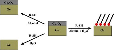 | ||
| Fig. 1 The importance of solubility on direct SAM deposition on Ge(100). Germanium oxide is soluble in water, while the alkanethiols are soluble in alcohols. A water/alcohol mixture can dissolve both the germanium oxide and enough alkanethiol to form SAMs. The unmixed solvents (and exposure in a stepwise fashion) do not produce SAMs. | ||
Kinetics of self-assembled monolayer deposition
A simple kinetic experiment was devised to monitor the growth of the monolayer as a function of solution exposure time and to determine the optimum deposition time, the results of which are shown in Fig. 2. Monolayer formation is monitored by analysis of the dynamic water contact angle (WCA), the general technique we use for tracking both the coverage and the quality of the film of individual samples. Full-coverage n-alkanethiolate SAMs are known to give water contact angles of >100°.31,102 The SAM deposition process on germanium is slower than alkanethiolate assembly on Au{111}. On gold, SAMs reach full coverage in seconds deposited from solutions at micromolar thiol concentrations.6 Monolayers on germanium form gradually between 10 and 1000 min of exposure to the solution; no further improvement is observed after 24 h. Some run-to-run variability is observed for the kinetics, but all samples display the same average WCA after 24 h. Analysis of these films by XPS reveals strong temperature dependence for final coverage, but only a weak dependence for WCA; this relationship will be described below. Measuring dynamic water contact angle on a bare, as-received germanium wafer is complicated by the solubility of the oxide. The first drop on a small sample will begin dissolving the oxide and adventitious material such that the second drop will be placed on a significantly more hydrophilic surface. The dynamic surface results in large uncertainty for measurements at low SAM coverage. We eliminated this variability by first stripping the oxide from the surface by exposure to a 1:1 ethanol–water solution overnight, which results in a highly hydrophilic surface; any increase in hydrophobicity is thus directly attributed to the deposition of C12 rather than a variable oxide/C12 surface. When directly preparing monolayers, this step is unnecessary, but was important for measurements of the kinetics at short deposition times.
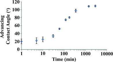 | ||
| Fig. 2 Kinetics of SAM formation on Ge(100), Ge(110), and Ge(111). Deposition is from 0.5 mM C12 solution in 1:1 ethanol–water, on surfaces etched for 24 h in 1:1 ethanol–water to give a hydrophilic surface devoid of germanium oxides. Advancing water contact angles (n = 3) are shown on a logarithmic time axis for clarity. The period of the most dramatic change occurs between 10 and 1000 min. | ||
Solvent-dependence for self-assembled monolayers on germanium
To test the hypothesis that SAM deposition occurs in the mixed-solvent system as a function of solubility, we designed an experiment to test WCA for SAMs formed after 24 h exposure to a variety of water/alcohol ratios. Three mixtures were investigated, using water and methanol, ethanol, or t-butanol (not shown, as no ratio gave a monolayer with a WCA > 100°) The “volcano plots” in Fig. 3 show a rise in SAM quality as the water content of the mixture increases. Methanol showed a moderately wider window of acceptable solution composition than ethanol; any mixture between 20% and 80% water formed SAMs. Ethanol had a narrower window of acceptable concentration, with full-coverage films only observed between 40% and 60% water. The third alcohol tested, t-butanol (not shown), did not form full-coverage films at any ratio, but showed the same overall shape; there was no SAM deposition at the extremes of concentration, but surfaces were moderately hydrophobic (∼80°) at a 1:1 t-butanol/water ratio.
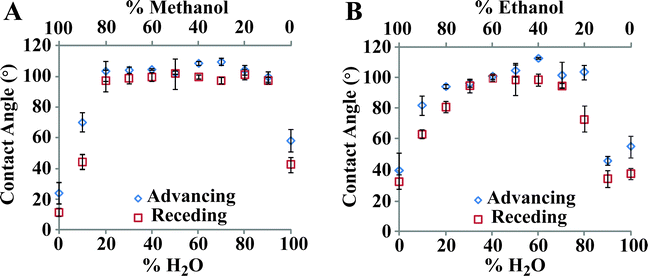 | ||
| Fig. 3 Dependence of SAM quality on mixed solvent ratio. The appropriate quantity of C12 is dissolved in (A) methanol or (B) ethanol, and then diluted with water to the selected volume and ratio. Methanol yields a consistently wider window of solvent composition than ethanol. | ||
There are two regimes of solvent ratio to consider; the low water/alcohol ratio case, where assembly is limited by germanium oxide solubility, and the high water/alcohol ratio case, where the alkanethiols are more sparsely soluble. In both cases, methanol shows a larger window for deposition of C12 monolayers (we prefer to use ethanol for its lower toxicity). At low water concentration, we suggest that germanium oxides are more soluble in the presence of methanol–water mixtures than in solutions containing either ethanol or t-butanol; the methanol–water solution can thus more effectively remove the native oxide when compared to the more hydrophobic alcohols. At 20% water, the methanol mixture forms full-coverage films.
For the high water concentration regime, we expected that the more hydrophobic alcohols (ethanol and t-butanol) would still permit satisfactory SAM deposition, as a more hydrophobic alcohol should keep the alkanethiols solvated at higher water concentrations. However, above 70% water there is a sharp decrease in film quality for the ethanol mixture, leading us to believe that the mechanism for alkanethiol delivery to the germanium surface is more complicated than a simple dependence on solubility. One possible mechanism is that alkanethiols are deposited from a stable emulsion or from micelles; such an effect would explain how films can be deposited even at concentration ratios where the alkanethiol is phase-separated as a cloudy suspension.
X-ray photoelectron spectroscopy analysis of self-assembled monolayers on germanium
While WCA is an excellent qualitative technique for monitoring relative surface characteristics, a quantitative technique is required to relate those values to the actual surface coverage and chemistry. X-ray photoelectron spectroscopy (XPS) is a surface-selective technique that enables observation of thin-film chemical composition on a wide variety of substrates. Here, we used XPS to monitor SAM formation and the concurrent removal of native germanium oxide (and adventitious carbon contamination). Fig. 4 shows the high-resolution spectra of the (A) C 1s, (B) S 2p, (C) Ge 2p, (D) Ge 3d, and (E) O 1s regions (survey spectra not shown). Table S1 (ESI†) in the electronic supplementary information summarizes fit peak energies for all regions. In each case, an overlay is prepared showing comparisons between the as-received germanium wafer, after oxide removal by a 1:1 water–ethanol solution, and after C12 SAM deposition at room temperature.
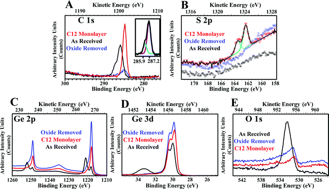 | ||
| Fig. 4 High-resolution XPS spectra collected for the regions specific to C 1s, S 2p, Ge 3d, O 1s, and Ge 2p. Each region is shown with its own arbitrary intensity scale. (A, C 1s) Adventitious carbon (black trace) is effectively eliminated by treatment with the water–ethanol mixture (blue trace), allowing a C12 SAM to form (red trace). Inset: C 1s peak of the Ge surface showing alkyl carbons and carbons attached to the Ge oxide surface. (B, S 2p) The C12 monolayer gives the expected response in the S 2p region, while the as-received and the cleaned wafers do not show the presence of any sulfur. (C, Ge 2p) Germanium oxide (black trace), primarily GeO2 (33.2 eV), is removed readily by water–ethanol treatment, leaving high-intensity peaks attributed to the bulk germanium crystal (blue trace). The intensity is attenuated by the presence of the SAM (red trace). (D, Ge 3d) The Ge 3d spectra provide information complementary to that of the Ge 2p spectra. Water treatment again eliminates the signal from GeO2 (blue trace). The Ge 3d doublet appears shifted slightly to lower binding energy. The intensity is again attenuated by the presence of the monolayer (red trace). (E, O 1s) The majority of the oxygen is attributed to native germanium oxide; after removal or SAM formation, remaining oxygen is attributed to residual alcohols or oxide reformation at defect sites before the samples were loaded into the XPS vacuum chamber. | ||
We first consider the spectra associated with the SAM elements, specifically the C 1s and S 2p regions (Fig. 4, top row). The as-received germanium wafers show considerable adventitious carbon, characterized by the relatively broad peak (Fig. 4A, black trace), a feature commonly observed on untreated germanium wafers.103 This peak is composed of two types of elemental carbon, at 285.9 eV (76.2%) and 287.2 eV (23.8%), corresponding to aliphatic carbons and Ge–O–C, respectively (Fig. 4A inset). Removing the oxide in the water–ethanol bath eliminates this feature; the majority of the carbon is adsorbed on the germanium oxide (Fig. 4A, blue trace). Upon SAM adsorption, a single sharp peak at 284.9 eV is observed, associated with carbon from the C12 monolayer (Fig. 4A, red trace).104,105 The presence of the Ge–S bond is confirmed by the S 2p3/2 and S 2p1/2 at 162.4 and 163.6 eV, respectively (Fig. 4B, red triangles) with a peak intensity ratio of 2:1; neither oxidized sulfur species nor unbound/atomic sulfur were observed.106 These characteristics are consistent with observations of thiolates on Au.31,104,107,108 No sulfur signal is detected on either the as-received or the oxide-removed wafers. Increasing the deposition temperature to 60 °C increases the total integrated peak area for the S 2p by a factor of two, as shown in Fig. 6. This will be discussed in detail below.
Next, we consider the spectra associated with germanium and its native oxide, the Ge 2p, Ge 3d, and O 1s regions (Fig. 4, bottom row). The Ge 2p spectra (Fig. 4C) show the progression of the SAM formation process. Two complementary regions are considered, the Ge 2p3/2 and 2p1/2 regions, which are separated by approximately 30 eV. Germanium is commonly present in several oxidation states, but is predominantly in the +4 oxidized state in native germanium oxide.90 The spectra of the as-received wafers show evidence of both oxidized (1220.9 and 1252.0 eV) germanium,73 and the buried, bulk germanium (1218.2 and 1249.2 eV). After the water–ethanol treatment, the peaks associated with germanium oxide are substantially decreased, while peaks associated with bulk germanium increase in intensity. The soluble germanium oxides have been removed, allowing emitted photoelectrons from the bulk germanium an unimpeded path to the detector. The presence of the residual germanium oxide shoulder is attributed to oxide reformation during the brief period of exposure experienced by the germanium wafer before it was loaded into the XPS vacuum chamber, as well as insoluble germanium(II) oxide. After deposition of the SAM, the intensity of the germanium signal decreases, attenuated by SAM thickness. The residual oxide is the primary suspect for the relatively short lifetime of SAMs on Ge (vide infra).
Analysis of the Ge 3d region (Fig. 4D) reveals complementary information. The Ge 3d5/2 (30.0 eV) and Ge 3d3/2 (30.6 eV) peaks are well-resolved, with peak splitting of 0.6 eV.73,85,109 The peak at 33.2 eV, which corresponds to oxidized germanium on the as-received wafer,110 is predominantly from GeO2 and was successfully removed after oxide removal or SAM deposition. Weak tails at higher binding energy presumably arises from oxidized germanium with lower oxidation states, especially +2.90,111,112 Removing the oxide layer shifts the Ge 3d doublet slightly to lower binding energy, a result of the loss of the passivation layer. No shift is observed after deposition of the SAM, although the expected decrease in intensity is observed.
The majority of the oxygen present in the film is removed with the oxide layer; the intense O 1s peak at 532.5 eV is absent from both the cleaned and SAM-modified surface (Fig. 4E). After oxide removal and SAM formation, asymmetric and low-intensity oxygen peaks around 531 eV correspond to the GeO region (530.8 eV). This species is insoluble in water, and is a primary suspect in the relatively short lifetimes of SAMs on Ge, as discussed below. Oxygen from germanium oxide reformation or residual adsorbed ethanol cannot be discounted.
Considerations for expanding the germanium self-assembly chemical library
Three decades of interest in thiol/metal SAM systems has resulted in a large chemical library of molecules for functional SAMs. We focused on a cross section of this library, covering some commonly used molecules and terminal functional groups.Unlike gold, which has limited chemistry and forms covalent bonds with few functional groups, the germanium surface is more reactive; chemical reactions with amides,113–115 organic alcohols,116,117 and other functional groups118–126 have been reported. Also, even small multifunctional molecules may straddle available binding sites,118 bidentate attachment is a concern when fabricating functional SAMs. Included here are XPS and WCA measurements of SAMs of 1-octadecanethiol (C18), 11-mercaptoundecanoic acid (MUDA), 1-mercaptoundecanol (MUDOL), and the internally functionalized 3-mercapto-N-nonylpropionamide (1ATC9). Water contact angles for these SAMs are collected in Table 1.
| Ge(100) | Ge(110) | Ge(111) | ||||
|---|---|---|---|---|---|---|
| θ a° | θ r° | θ a° | θ r° | θ a° | θ r° | |
|
a All SAMs deposited from 1:1 water–ethanol solutions for 24 h.
|
||||||
| C12 25 °C | 109.9 ± 0.1 | 101.9 ± 0.1 | 107.1 ± 0.2 | 100.9 ± 0.1 | 105.6 ± 0.1 | 104.0 ± 0.1 |
| C12 60 °C | 103.5 ± 0.1 | 100.2 ± 0.1 | 105.1 ± 0.1 | 97.8 ± 0.1 | 107.1 ± 0.1 | 102.6 ± 0.1 |
| C18 25 °C | 106.5 ± 0.1 | 98.8 ± 0.1 | 107.6 ± 0.1 | 97.5 ± 0.1 | 105.9 ± 0.1 | 100.7 ± 0.2 |
| C18 60 °C | 116.7 ± 0.1 | 109.6 ± 0.1 | 110.7 ± 0.1 | 106.1 ± 0.1 | 108.4 ± 0.1 | 105.2 ± 0.2 |
| MUDA 25 °C | 70.6 ± 0.1 | 56.2 ± 0.1 | 59.9 ± 0.4 | 46.8 ± 0.1 | 66.5 ± 0.3 | 59.8 ± 0.3 |
| MUDOL 25 °C | 75.1 ± 0.1 | 69.9 ± 0.3 | 65.6 ± 0.2 | 50.0 ± 0.2 | 58.7 ± 0.3 | 51.4 ± 0.3 |
| 1ATC9 25 °C | 97.4 ± 0.1 | 91.7 ± 0.1 | 90.6 ± 0.8 | 93.9 ± 0.5 | 98.7 ± 0.2 | 93.2 ± 0.1 |
Solubility in polar solvents decreases with increasing alkyl chain length; while C12 is soluble in the water–ethanol mix at room temperature, C18 precipitates on the addition of water. As with C12, the sparsely soluble C18 suspension will produce a hydrophobic, C18-terminated Ge surface with WCA >105°. Elevating the incubation temperature to 60 °C increases C18 solubility, resulting in a monolayer with higher WCA (>115°) and coverage (other important details related to temperature and coverage are addressed below).
The S 2p spectra of MUDA, MUDOL, C18, and 1ATC9 are shown in Fig. 5, and are similar in absolute intensity and peak ratio to those for the C12 monolayers (shown in Fig. 4B, red trace). Importantly, no unbound sulfur is present, providing evidence that the films are primarily attached by Ge–S binding, rather than side reactions involving the tail groups. The C 1s XPS spectra for these adsorbates (shown in Figure S1, ESI†) show moderately lower intensities when compared to C12, but suggest similar overall coverages. As expected from its longer alkyl chain, C18 shows higher C 1s intensities in XPS and higher WCA. For the functional molecules, MUDA, MUDOL, and 1ATC9, WCA measurements deviate from reported values on gold, as shown in Table 1, with MUDA and MUDOL giving higher than expected WCA values, and 1ATC9 giving lower than expected values. These results suggest sub-monolayer coverage for all these molecules, leaving alkyl chains exposed at the surface between polar functional groups.14,16,127,128 The WCA for 1ATC9 was slightly lower than expected for the same SAM on gold, likely a result of exposed amide or germanium regions.129,130
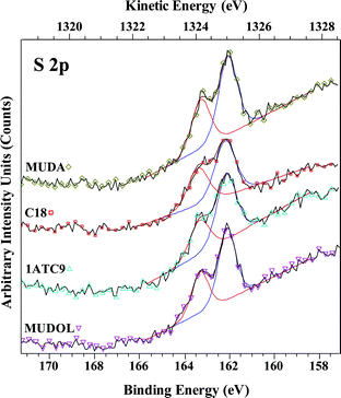 | ||
| Fig. 5 Comparison of high-resolution S 2p regions for various SAMs: 1-octadecanethiol (C18), 11-mercaptoundecanoic acid (MUDA), 1-mercaptoundecanol (MUDOL), and 3-mercapto-N-nonylpropionamide (1ATC9), on Ge(100) deposited at 25 °C. Absolute integrated peak intensity is similar for each SAM, and matches that for C12 (shown in Fig. 4B, red trace). The absence of unbound sulfur shows that SAMs are attached primarily via Ge–S binding, although the possibility for bidentate interactions are not excluded for MUDA, MUDOL, and 1ATC9 monolayers (vide infra). | ||
SAM formation at elevated temperature
Increasing the incubation temperature for gold-thiol self-assembly improves SAM order; faster exchange at defect sites results in larger average domain sizes and lower abundances of defects.6 Elevating temperature to 60 °C likewise improves the quality of SAMs on Ge, measured by WCA and XPS. Fig. 6 shows the XPS spectra of the S 2p and C 1s regions for C12 and C18 monolayers on Ge(100) deposited at 60 °C. Intensity increases substantially in both regions at this temperature. An integrated area increase by a factor of two for the S 2p region is consistent with doubling the sulfur coverage. This observation leads to an important revelation: despite the high apparent quality of the films, coverages reach a maximum of 50% when deposition is at room temperature, while increasing the temperature leads to (nominally) 100% coverage. The WCA for C18 SAMs increases significantly, but no systematic improvement is noted for C12 SAMs.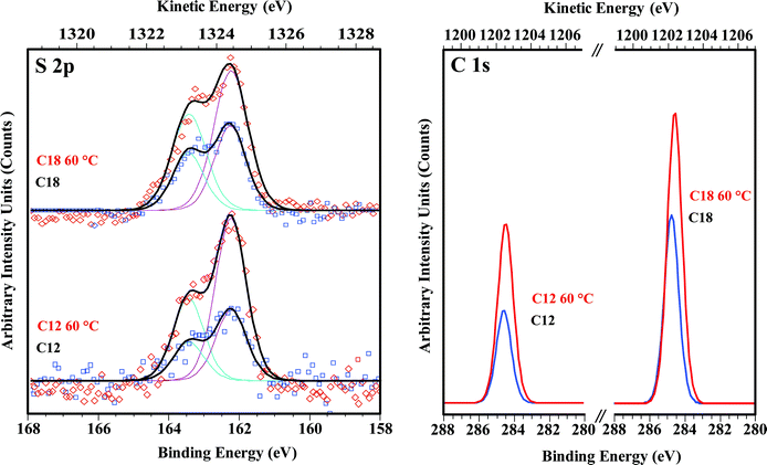 | ||
| Fig. 6 High-resolution S 2p (left) and C 1s (right) XPS spectra, comparing C12 and C18 SAMs on Ge(100) formed at room-temperature and at 60 °C. Sulfur and carbon intensity increases by approximately a factor of two when a SAM is deposited at 60 °C, indicating 50% coverage for room temperature depositions, and full coverage for depositions at 60 °C. | ||
The Ge(100) surface reconstructs with pairs of adjacent Ge atoms forming dimers (Ge(100)-(2 × 1)).119,131,132 Charge transfer between the atoms (equivalent to ∼0.1 e) causes the dimers to buckle, with the more negative member of the pair protruding from the lattice and the more positive member closer to the bulk. The buckled pairs can be either symmetric, the p(2 × 1) structure, or asymmetric, the c(4 × 2) structure. Theoretical and experimental investigations by Bent and coworkers provide the framework for explaining the observed increases in coverage with elevated temperature.92 Theoretical predictions for thiol substitution reactions on halide-terminated germanium surfaces indicate that the germanium dimer bond remains intact after reaction with thiols, and that the reaction will be favoured at higher temperature; both results are in agreement with our experimental observations. At room temperature, we speculate that the thiol bonds at the electrophile, transferring the proton to the nucleophilic position. Once it reaches 50% coverage, there are no remaining electrophiles, and the reaction slows dramatically. At 60 °C, the thiol is able to react with all available germanium sites, as opposed to only the electrophilic sites, in line with theoretical predictions.92 The fate of the hydrogen atom is speculative, as is also typically the case for thiol adsorption on gold.6 A schematic of the proposed mechanism for explaining the trend in temperature-dependent coverage is shown in Fig. 7. These results are restricted to the Ge(100) surface; further studies will be required to test whether the same trends hold for Ge(111) and Ge(110), to determine the role of thiolate exchange at elevated temperature, and to determine how the bare Ge surface differs from halogenated and hydrogenated Ge.
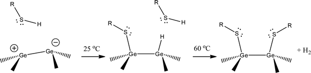 | ||
| Fig. 7 Proposed reaction pathway for thiolate SAM formation on Ge(100). The Ge(100) surface reconstructs to form dimer pairs. Charge transfer (∼0.1 e) causes the dimer pair to buckle, with the less-protruding atom more electrophilic. At room temperature, the thiol reacts at one position, resulting in a 50% coverage film. At higher temperatures, the second position becomes energetically accessible, resulting in full monolayer coverage. The role and destination of the hydrogen atom is speculative, as is also typically the case for thiol adsorption on gold. | ||
Measurements for WCA of all investigated molecules are included in Table 1. While coverage and WCA increase at elevated deposition temperature for C12 and C18, results for other functionalized films are inconsistent. This was confirmed through XPS analyses, where the functional films did not display significant increases in sulfur intensity after heating. We suspect side reactions between the tail groups and the germanium surface at higher temperature, but this work provides a starting point for future self-assembly studies on germanium surfaces.
Despite the differences in film coverage at elevated temperature, SAMs formed at elevated temperature do not show significantly longer lifetimes than those formed at lower temperature. Contact angle and ellipsometric observations led Ardalan et al. to suggest that defects in the SAM eventually provide access of atmospheric oxygen to the germanium substrate, allowing reformation of the germanium oxide;90,133 our measurements support this notion. We include measurements and discussion of SAM stability in the electronic supporting information†.
Gentle in situ etch and passivation
Germanium oxide is incommensurate to the underlying germanium. Despite the excellent quality of commercially available semiconductor wafers, a roughened, defect-rich surface results from direct germanium oxide removal. When a stepwise method for SAM deposition is used, a cyclic treatment by hydrogen peroxide and mineral acids is often employed for a clean and smooth surface amenable for further functionalization. A disadvantage of this process is that any defects present on the passivated surface will be perpetuated through to the final film, as the process possesses no inherent capacity for self-healing.The mixed-solvent method described here combines the slow etch rate of water and simultaneous passivation by alkanethiol, creating conditions for a gentle, self-terminating in situ etch of the surface. Supplemental Figures S2, S3 (ESI†) depict AFM and STM images tracking the topography of the surface during the SAM formation process. Commercial, polished wafers are extraordinarily flat;134 the measured RMS roughness for a 1 μm region is approximately 2 Å. Exposure to the water–ethanol solution for 24 h slightly alters the surface, with surface features appearing more rounded. Deposition of a C12 SAM returns the surface to near its original flatness, with no measured trends in RMS roughness or obvious changes in surface topography. Surface features created by water etch of the germanium wafer are healed over the course of SAM deposition. We postulate that defect regions not protected by thiol functionalization remain susceptible to reoxidation. By performing the oxide etch while depositing the passivation layer, defects that reoxidize are stripped and then eventually functionalized without removing large amounts of material. This technique is thus ideal for forming SAMs on nanoscale germanium structures where a more aggressive etch is undesirable.
Despite preserving the excellent roughness characteristics of germanium wafers by this method, the surfaces are not atomically flat, as illustrated by the STM image in Figure S3, ESI†. However, the described deposition technique is compatible with halogenated surfaces, so an atomically flat and halogenated surface may retain its nanoscale features during SAM deposition, which in turn could improve the nanoscale order of the monolayer.131
Conclusions and prospects
We developed a simple, robust method for the deposition of high-quality SAMs on Ge(100). We focused our analytical efforts on C12 monolayers on Ge(100), but successfully expanded the technique to include Ge(111) and Ge(110) and functionalized alkanethiol derivatives. The critical factor for the deposition process is the adjustment of solvent composition to solvate both substrate germanium oxide and the (typically) nonpolar adsorbate. Temperature plays a critical role in the final coverage of the attached film. When deposited at room temperature, the film reaches a maximum of 50% coverage, while increasing the temperature to 60 °C results in a full-coverage monolayer. We used a simple model of unequal reactivity at Ge surface dimers to explain SAM formation on germanium, where thiol reaction at the nucleophilic position is spontaneous only at elevated temperature. This model conveniently explains the observed temperature dependence of the reaction on the p(2 × 1) reconstruction of Ge(100), but the atomic-scale roughness of the germanium surface and similar behaviour on other germanium crystal faces necessitates further study to exploit the reaction mechanism for new directions in designed self-assembled systems on semiconductor surfaces. Long-term stability and nanoscale order of the films remain important goals in order for SAMs on germanium to find diverse technological applications, with residual GeO at defects suspect for speeding degradation of the monolayers.Our strategy for expanding self-assembly of monolayers on germanium was to adjust reaction conditions such that the overall process mimics the alkanethiol assembly on gold and maintains the advantages of that system. Germanium wafers with low roughness surfaces are commercially available in a variety of crystallographic orientations and doping profiles, and all are viable substrates for SAM preparation. Our process for forming SAMs on germanium is completed in a simple single step, and coverage of either 50% or 100% can be selected by temperature control. Alkanethiols are able to displace contaminants on the germanium surface, as the passivating oxide and adventitious material is dissolved as part of the in situ etch of the germanium surface, and because of the high bond strength between the thiolate and germanium. Finally, we have demonstrated that functional alkanethiol derivatives are viable adsorbates for the preparation of functional SAMs on germanium.
Acknowledgements
We thank the National Science Foundation, the Kavli Foundation, and Penn State's National Nanotechnology Infrastructure Network for their continued support of this work. Additionally, the Penn State University Materials Characterization Laboratory and especially Dr Thomas A. Daniel are gratefully acknowledged for data collection and XPS analysis. Lastly, the authors thank David G. McMillan for technical support and assistance.Notes and references
- R. G. Nuzzo and D. L. Allara, J. Am. Chem. Soc., 1983, 105, 4481–4483 CrossRef CAS.
- D. L. Allara and R. G. Nuzzo, Langmuir, 1985, 1, 52–66 CrossRef CAS.
- G. E. Poirier and M. J. Tarlov, Langmuir, 1994, 10, 2853–2856 CrossRef CAS.
- A. Ulman, Chem. Rev., 1996, 96, 1533–1554 CrossRef CAS.
- R. K. Smith, P. A. Lewis and P. S. Weiss, Prog. Surf. Sci., 2004, 75, 1–68 CrossRef CAS.
- J. C. Love, L. A. Estroff, J. K. Kriebel, R. G. Nuzzo and G. M. Whitesides, Chem. Rev., 2005, 105, 1103–1169 CrossRef CAS.
- S. D. Evans, E. Urankar, A. Ulman and N. Ferris, J. Am. Chem. Soc., 1991, 113, 4121–4131 CrossRef.
- J. M. Tour, L. Jones, D. L. Pearson, J. J. S. Lamba, T. P. Burgin, G. M. Whitesides, D. L. Allara, A. N. Parikh and S. V. Atre, J. Am. Chem. Soc., 1995, 117, 9529–9534 CrossRef CAS.
- R. R. Kolega and J. B. Schlenoff, Langmuir, 1998, 14, 5469–5478 CrossRef CAS.
- L. J. Yeager, F. Saeki, K. Shelly, M. F. Hawthorne and R. L. Garrell, J. Am. Chem. Soc., 1998, 120, 9961–9962 CrossRef CAS.
- A. A. Dameron, L. F. Charles and P. S. Weiss, J. Am. Chem. Soc., 2005, 127, 8697–8704 CrossRef CAS.
- M. Kim, J. N. Hohman, E. I. Morin, T. A. Daniel and P. S. Weiss, J. Phys. Chem. A, 2009, 113, 3895–3903 CrossRef CAS.
- D. Kafer, G. Witte, P. Cyganik, A. Terfort and C. Woll, J. Am. Chem. Soc., 2006, 128, 1723–1732 CrossRef.
- H. J. Himmel, A. Terfort and C. Woll, J. Am. Chem. Soc., 1998, 120, 12069–12074 CrossRef CAS.
- O. Dannenberger, K. Weiss, H. J. Himmel, B. Jager, M. Buck and C. Woll, Thin Solid Films, 1997, 307, 183–191 CrossRef CAS.
- R. Arnold, W. Azzam, A. Terfort and C. Woll, Langmuir, 2002, 18, 3980–3992 CrossRef CAS.
- J. N. Hohman, P. P. Zhang, E. I. Morin, P. Han, M. Kim, A. R. Kurland, P. D. McClanahan, V. P. Balema and P. S. Weiss, ACS Nano, 2009, 3, 527–536 CrossRef CAS.
- A. Vaish, M. J. Shuster, S. Cheunkar, Y. S. Singh, P. S. Weiss and A. M. Andrews, ACS Chem. Neurosci., 2010, 1, 495–504 Search PubMed.
- G. Y. Liu, S. Xu and Y. L. Qian, Acc. Chem. Res., 2000, 33, 457–466 CrossRef CAS.
- S. Kramer, R. R. Fuierer and C. B. Gorman, Chem. Rev., 2003, 103, 4367–4418 CrossRef.
- H. M. Saavedra, T. J. Mullen, P. P. Zhang, D. C. Dewey, S. A. Claridge and P. S. Weiss, Rep. Prog. Phys., 2010, 73, 036501 CrossRef.
- Y. H. Wang, C. A. Mirkin and S. J. Park, ACS Nano, 2009, 3, 1049–1056 CrossRef CAS.
- C. A. Mirkin, ACS Nano, 2007, 1, 79–83 CrossRef CAS.
- Y. N. Xia, J. A. Rogers, K. E. Paul and G. M. Whitesides, Chem. Rev., 1999, 99, 1823–1848 CrossRef CAS.
- R. D. Piner, J. Zhu, F. Xu, S. Hong and C. A. Mirkin, Science, 1999, 283, 661–663 CrossRef CAS.
- A. A. Dameron, J. R. Hampton, R. K. Smith, T. J. Mullen, S. D. Gillmor and P. S. Weiss, Nano Lett., 2005, 5, 1834–1837 CrossRef CAS.
- T. J. Mullen, C. Srinivasan, J. N. Hohman, S. D. Gillmor, M. J. Shuster, M. W. Horn, A. M. Andrews and P. S. Weiss, Appl. Phys. Lett., 2007, 90, 063114 CrossRef.
- J. L. Wilbur, A. Kumar, E. Kim and G. M. Whitesides, Adv. Mater., 1994, 6, 600–604 CAS.
- M. E. Anderson, C. Srinivasan, J. N. Hohman, E. M. Carter, M. W. Horn and P. S. Weiss, Adv. Mater., 2006, 18, 3258–3260 CrossRef CAS.
- C. Srinivasan, T. J. Mullen, J. N. Hohman, M. E. Anderson, A. A. Dameron, A. M. Andrews, E. C. Dickey, M. W. Horn and P. S. Weiss, ACS Nano, 2007, 1, 191–201 CrossRef CAS.
- C. D. Bain, E. B. Troughton, Y. T. Tao, J. Evall, G. M. Whitesides and R. G. Nuzzo, J. Am. Chem. Soc., 1989, 111, 321–335 CrossRef CAS.
- D. P. Woodruff, Phys. Chem. Chem. Phys., 2008, 10, 7211–7221 RSC.
- H. Sellers, A. Ulman, Y. Shnidman and J. E. Eilers, J. Am. Chem. Soc., 1993, 115, 9389–9401 CrossRef CAS.
- J. B. Schlenoff, M. Li and H. Ly, J. Am. Chem. Soc., 1995, 117, 12528–12536 CrossRef CAS.
- J. C. Love, D. B. Wolfe, M. L. Chabinyc, K. E. Paul and G. M. Whitesides, J. Am. Chem. Soc., 2002, 124, 1576–1577 CrossRef CAS.
- E. Sabatani, I. Rubinstein, R. Maoz and J. Sagiv, J. Electroanal. Chem., 1987, 219, 365–371 CrossRef CAS.
- H. Ron and I. Rubinstein, Langmuir, 1994, 10, 4566–4573 CrossRef CAS.
- B. Sun, S. E. Baker, J. E. Butler, H. Kim, J. N. Russell, L. Shang, K. Y. Tse, W. S. Yang and R. J. Hamers, Diamond Relat. Mater., 2007, 16, 1608–1615 CrossRef CAS.
- M. R. Linford and C. E. D. Chidsey, J. Am. Chem. Soc., 1993, 115, 12631–12632 CrossRef CAS.
- M. R. Linford, P. Fenter, P. M. Eisenberger and C. E. D. Chidsey, J. Am. Chem. Soc., 1995, 117, 3145–3155 CrossRef CAS.
- T. A. Tanzer, P. W. Bohn, I. V. Roshchin, L. H. Greene and J. F. Klem, Appl. Phys. Lett., 1999, 75, 2794–2796 CrossRef CAS.
- S. M. Han, W. R. Ashurst, C. Carraro and R. Maboudian, J. Am. Chem. Soc., 2001, 123, 2422–2425 CrossRef.
- M. Schvartzman, V. Sidorov, D. Ritter and Y. Paz, J. Vac. Sci. Technol., B, 2003, 21, 148–155 CrossRef CAS.
- V. M. Bermudez, Langmuir, 2003, 19, 6813–6819 CrossRef CAS.
- M. Zharnikov, A. Kuller, A. Shaporenko, E. Schmidt and W. Eck, Langmuir, 2003, 19, 4682–4687 CrossRef CAS.
- K. Moumanis, X. Ding, J. J. Dubowski and E. H. Frost, J. Appl. Phys., 2006, 100, 034702 CrossRef.
- X. M. Ding, K. Moumanis, J. J. Dubowski, L. Tay and N. L. Rowell, J. Appl. Phys., 2006, 99, 054701 CrossRef.
- H. Kim, P. E. Colavita, K. M. Metz, B. M. Nichols, B. Sun, J. Uhlrich, X. Wang, T. F. Kuech and R. J. Hamers, Langmuir, 2006, 22, 8121–8126 CrossRef CAS.
- R. Flores-Perez, D. Y. Zemlyanov and A. Ivanisevic, J. Phys. Chem. C, 2008, 112, 2147–2155 CrossRef CAS.
- D. Zerulla and T. Chasse, J. Electron Spectrosc. Relat. Phenom., 2009, 172, 78–87 CrossRef CAS.
- S. R. Lunt, G. N. Ryba, P. G. Santangelo and N. S. Lewis, J. Appl. Phys., 1991, 70, 7449–7465 CrossRef CAS.
- O. S. Nakagawa, S. Ashok, C. W. Sheen, J. Martensson and D. L. Allara, Jpn. J. Appl. Phys., Part 1, 1991, 30, 3759–3762 CAS.
- S. F. Bent, ACS Nano, 2007, 1, 10–12 CrossRef CAS.
- C. L. McGuiness, A. Shaporenko, M. Zharnikov, A. V. Walker and D. L. Allara, J. Phys. Chem. C, 2007, 111, 4226–4234 CrossRef CAS.
- C. L. McGuiness, D. Blasini, J. P. Masejewski, S. Uppili, O. M. Cabarcos, D. Smilgies and D. L. Allara, ACS Nano, 2007, 1, 30–49 CrossRef CAS.
- J. Sagiv, J. Am. Chem. Soc., 1980, 102, 92–98 CrossRef CAS.
- A. Zeira, D. Chowdhury, R. Maoz and J. Sagiv, ACS Nano, 2008, 2, 2554–2568 CrossRef CAS.
- R. Maoz and J. Sagiv, Adv. Mater., 1998, 10, 580–584 CrossRef CAS.
- B. M. Nichols, J. E. Butler, J. N. Russell and R. J. Hamers, J. Phys. Chem. B, 2005, 109, 20938–20947 CrossRef CAS.
- B. M. Nichols, K. M. Metz, K. Y. Tse, J. E. Butler, J. N. Russell and R. J. Hamers, J. Phys. Chem. B, 2006, 110, 16535–16543 CrossRef CAS.
- T. Strother, T. Knickerbocker, J. N. Russell, J. E. Butler, L. M. Smith and R. J. Hamers, Langmuir, 2002, 18, 968–971 CrossRef CAS.
- M. Volmer, M. Stratmann and H. Viefhaus, Surf. Interface Anal., 1990, 16, 278–282 CAS.
- M. Wolpers, H. Viefhaus and M. Stratmann, Appl. Surf. Sci., 1990, 45, 167–170 CrossRef CAS.
- A. Mahapatro, D. M. Johnson, D. N. Patel, M. D. Feldman, A. A. Ayon and C. M. Agrawal, Langmuir, 2006, 22, 901–905 CrossRef CAS.
- K. Cimatu and S. Baldelli, J. Phys. Chem. C, 2007, 111, 7137–7143 CrossRef CAS.
- H. Zhang, C. Romero and S. Baldelli, J. Phys. Chem. B, 2005, 109, 15520–15530 CrossRef CAS.
- H. Ron, H. Cohen, S. Matlis, M. Rappaport and I. Rubinstein, J. Phys. Chem. B, 1998, 102, 9861–9869 CrossRef CAS.
- R. G. Nuzzo, B. R. Zegarski and L. H. Dubois, J. Am. Chem. Soc., 1987, 109, 733–740 CrossRef CAS.
- J. Bardeen and W. H. Brattain, Phys. Rev., 1948, 74, 230–231 CrossRef.
- B. Onsia, T. Conard, S. De Gendt, M. Heyns, I. Hoflijk, P. Mertens, M. Meuris, G. Raskin, S. Sioncke, I. Teerlinck, A. Theuwis, J. Van Steenbergen and C. Vinckier, in Ultra Clean Processing of Silicon Surfaces VII, ed. P. Mertens, M. Meuris and M. Heyns, Trans Tech Publications Ltd, Zurich-Uetikon, 2005, vol. 103–104, pp. 27–30 Search PubMed.
- S. Rivillon, Y. J. Chabal, F. Amy and A. Kahn, Appl. Phys. Lett., 2005, 87, 253101 CrossRef.
- K. Prabhakaran, F. Maeda, Y. Watanabe and T. Ogino, Appl. Phys. Lett., 2000, 76, 2244–2246 CrossRef CAS.
- K. Prabhakaran and T. Ogino, Surf. Sci., 1995, 325, 263–271 CrossRef CAS.
- P. W. Loscutoff and S. F. Bent, Annu. Rev. Phys. Chem., 2006, 57, 467–495 CrossRef CAS.
- D. Misra, R. Garg, P. Srinivasan, N. Rahim and N. A. Chowdhury, Mater. Sci. Semicond. Process., 2006, 9, 741–748 CrossRef CAS.
- P. P. Debye and E. M. Conwell, Phys. Rev., 1954, 93, 693–706 CrossRef CAS.
- C. Hilsum, Electron. Lett., 1974, 10, 259–260 CrossRef CAS.
- C. Jacoboni, F. Nava, C. Canali and G. Ottaviani, Phys. Rev. B, 1981, 24, 1014–1026 CrossRef CAS.
- G. W. Cullen, J. A. Amick and D. Gerlich, J. Electrochem. Soc., 1962, 109, 124–127 CrossRef.
- D. Knapp, B. S. Brunschwig and N. S. Lewis, J. Phys. Chem. C, 2010, 114, 12300–12307 CrossRef CAS.
- K. Choi and J. M. Buriak, Langmuir, 2000, 16, 7737–7741 CrossRef CAS.
- Z. H. Lu, Appl. Phys. Lett., 1996, 68, 520–522 CrossRef CAS.
- M. Gothelid, G. LeLay, C. Wigren, M. Bjorkqvist and U. O. Karlsson, Surf. Sci., 1997, 371, 264–276 CrossRef.
- J. Roche, P. Ryan and G. J. Hughes, Appl. Surf. Sci., 2001, 174, 271–274 CrossRef CAS.
- T. Hanrath and B. A. Korgel, J. Am. Chem. Soc., 2004, 126, 15466–15472 CrossRef CAS.
- M. Gothelid, G. LeLay, C. Wigren, M. Bjorkqvist, M. Rad and U. O. Karlsson, Appl. Surf. Sci., 1997, 115, 87–95 CrossRef CAS.
- T. Weser, A. Bogen, B. Konrad, R. D. Schnell, C. A. Schug and W. Steinmann, Phys. Rev. B, 1987, 35, 8184 CrossRef CAS.
- T. Maeda, S. Takagi, T. Ohnishi and M. Lippmaa, Mater. Sci. Semicond. Process., 2006, 9, 706–710 CrossRef CAS.
- M. R. Kosuri, R. Cone, Q. M. Li, S. M. Han, B. C. Bunker and T. M. Mayer, Langmuir, 2004, 20, 835–840 CrossRef CAS.
- P. Ardalan, C. B. Musgrave and S. F. Bent, Langmuir, 2009, 25, 2013–2025 CrossRef CAS.
- M. Lommel, P. Hönicke, M. Kolbe, M. Müller, F. Reinhardt, P. Möbus, E. Mankel, B. Beckhoff and B. O. Kolbesen, Solid State Phenom., 2009, 145, 169–172 CrossRef.
- P. Ardalan, Y. Sun, P. Pianetta, C. B. Musgrave and S. F. Bent, Langmuir, 2010, 26, 8419–8429 CrossRef CAS.
- J. L. He, Z. H. Lu, S. A. Mitchell and D. D. M. Wayner, J. Am. Chem. Soc., 1998, 120, 2660–2661 CrossRef CAS.
- Y. H. Min, S. J. Jung, Y. S. Youn, D. H. Kim and S. Kim, J. Am. Chem. Soc., 2010, 132, 9014–9019 CrossRef CAS.
- J. S. Kachian, J. Tannaci, R. J. Wright, T. D. Tilley and S. F. Bent, Langmuir, 2010, 27, 179–186.
- G. Collins, P. Fleming, S. Barth, C. O'Dwyer, J. J. Boland, M. A. Morris and J. D. Holmes, Chem. Mater., 2010, 22, 6370–6377 CrossRef CAS.
- G. C. Benson and O. Kiyohara, J. Solution Chem., 1980, 9, 791–804 CrossRef CAS.
- D. A. Shirley, Phys. Rev. B: Solid State, 1972, 5, 4709–4714 CrossRef.
- J. F. Moulder, Handbook of X-Ray Photoelectron Spectroscopy: A Reference Book of Standard Spectra for Identification and Interpretation of XPS Data, Perkin-Elmer Corporation, Physical Electronics Division, Eden Prairie, MN, 1992 Search PubMed.
- I. Horcas, R. Fernandez, J. M. Gomez-Rodriguez, J. Colchero, J. Gomez-Herrero and A. M. Baro, Rev. Sci. Instrum., 2007, 78, 013705 CrossRef CAS.
- L. A. Bumm, J. J. Arnold, L. F. Charles, T. D. Dunbar, D. L. Allara and P. S. Weiss, J. Am. Chem. Soc., 1999, 121, 8017–8021 CrossRef CAS.
- C. D. Bain and G. M. Whitesides, Science, 1988, 240, 62–63 CrossRef CAS.
- H. Okumura, T. Akane and S. Matsumoto, Appl. Surf. Sci., 1998, 125, 125–128 CrossRef CAS.
- P. E. Laibinis, C. D. Bain and G. M. Whitesides, J. Phys. Chem., 1991, 95, 7017–7021 CrossRef CAS.
- R. G. Nuzzo, L. H. Dubois and D. L. Allara, J. Am. Chem. Soc., 1990, 112, 558–569 CrossRef CAS.
- T. Ishida, N. Choi, W. Mizutani, H. Tokumoto, I. Kojima, H. Azehara, H. Hokari, U. Akiba and M. Fujihira, Langmuir, 1999, 15, 6799–6806 CrossRef CAS.
- H. A. Biebuyck, C. D. Bian and G. M. Whitesides, Langmuir, 1994, 10, 1825–1831 CrossRef CAS.
- J. P. Folkers, P. E. Laibinis and G. M. Whitesides, Langmuir, 1992, 8, 1330–1341 CrossRef CAS.
- N. Tabet, M. Faiz, N. M. Hamdan and Z. Hussain, Surf. Sci., 2003, 523, 68–72 CrossRef CAS.
- K. Prabhakaran and T. Ogino, Surf. Sci., 1995, 325, 263–271 CrossRef CAS.
- S. Y. Sun, Y. Sun, Z. Liu, D. I. Lee, S. Peterson and P. Pianetta, Appl. Phys. Lett., 2006, 88, 021903 CrossRef.
- H. Adhikari, P. C. McIntyre, S. Sun, P. Pianetta and C. E. D. Chidsey, Appl. Phys. Lett., 2005, 87, 263109 CrossRef.
- A. J. Keung, M. A. Filler and S. F. Bent, J. Phys. Chem. C, 2006, 111, 411–419 Search PubMed.
- A. J. Keung, M. A. Filler, D. W. Porter and S. F. Bent, Surf. Sci., 2005, 599, 41–54 CrossRef CAS.
- A. J. Keung, M. A. Filler and S. F. Bent, J. Phys. Chem. C, 2007, 111, 411–419 CrossRef CAS.
- S.-S. Bae, D. H. Kim, A. Kim, Jung, S. Hong and S. Kim, J. Phys. Chem. C, 2007, 111, 15013–15019 CrossRef CAS.
- J. S. Kachian and S. F. Bent, J. Am. Chem. Soc., 2009, 131, 7005–7015 CrossRef CAS.
- M. A. Filler, J. A. Van Deventer, A. J. Keung and S. F. Bent, J. Am. Chem. Soc., 2006, 128, 770–779 CrossRef CAS.
- P. W. Loscutoff and S. F. Bent, Annu. Rev. Phys. Chem., 2006, 57, 467–495 CrossRef CAS.
- M. A. Filler, A. J. Keung, D. W. Porter and S. F. Bent, J. Phys. Chem. B, 2006, 110, 4115–4124 CrossRef CAS.
- J. S. Kachian, K. T. Wong and S. F. Bent, Acc. Chem. Res., 2010, 43, 346–355 CrossRef CAS.
- P. W. Loscutoff, K. T. Wong and S. F. Bent, Surf. Sci., 2010, 604, 1791–1799 CrossRef CAS.
- Y. S. Youn, S. J. Jung, H. Lee and S. Kim, Langmuir, 2009, 25, 7438–7442 CrossRef CAS.
- D. H. Kim, S. S. Bae, S. Hong and S. Kim, Surf. Sci., 2010, 604, 129–135 CrossRef CAS.
- S. Park, S. Yang, N. Shin, E. Lee and H. Lee, J. Phys. Chem. C, 2010, 114, 14528–14531 CAS.
- Y. S. Youn, H. Lee and S. Kim, ChemPhysChem, 2010, 11, 354–356 CrossRef CAS.
- Y. Wang, Z. Zhang, V. Jain, J. Yi, S. Mueller, J. Sokolov, Z. Liu, K. Levon, B. Rigas and M. H. Rafailovich, Sens. Actuators, B, 2010, 146, 381–387 CrossRef.
- M. S. Wang, L. B. Palmer, J. D. Schwartz and A. Razatos, Langmuir, 2004, 20, 7753–7759 CrossRef CAS.
- R. S. Clegg and J. E. Hutchison, J. Am. Chem. Soc., 1999, 121, 5319–5327 CrossRef CAS.
- S. W. Tamchang, H. A. Biebuyck, G. M. Whitesides, N. Jeon and R. G. Nuzzo, Langmuir, 1995, 11, 4371–4382 CrossRef CAS.
- J. S. Hovis, R. J. Hamers and C. M. Greenlief, Surf. Sci., 1999, 440, L815–L819 CrossRef CAS.
- H. J. W. Zandvliet, Phys. Rep., 2003, 388, 1–40 CrossRef CAS.
- A. J. Mayne, F. Rose and G. Dujardin, Surf. Sci., 2003, 523, 157–167 CrossRef CAS.
- C. Teichert, J. F. Mackay, D. E. Savage, M. G. Lagally, M. Brohl and P. Wagner, Appl. Phys. Lett., 1995, 66, 2346–2348 CrossRef CAS.
Footnote |
| † Electronic supplementary information (ESI) available: Local probe images of modified germanium surfaces, additional C 1s spectra for functional monolayers, and discussion of monolayer stability. See DOI: 10.1039/c1sc00115a |
| This journal is © The Royal Society of Chemistry 2011 |