In situ monitoring of polymer redox states by resonance μRaman spectroscopy and its applications in polymer modified microfluidic channels†
Hella
Logtenberg
a,
Laurens-Jan C.
Jellema
b,
Maria J.
Lopez-Martinez
b,
Jetsuda
Areephong
a,
Elisabeth
Verpoorte
b,
Ben L.
Feringa
a and
Wesley R.
Browne
*a
aCenter for Systems Chemistry, Stratingh Institute for Chemistry, University of Groningen, Nijenborgh 4, 9747 AG, Groningen, The Netherlands. E-mail: w.r.browne@rug.nl
bDepartment of Pharmacy, University of Groningen, Antonius Deusinglaan 1, 9713 AV, Groningen, The Netherlands
First published on 20th October 2011
Abstract
We report the application of multi-wavelength resonance Raman (rR) spectroscopy for the characterisation of vinyl-bridged polysexithiophene films formed by electropolymerisation on gold electrodes. Resonance Raman spectroscopy of the neutral, polaronic and bipolaronic states of the polymer were determined by in situ μRaman spectroelectrochemistry. In particular the differences in the UV/Vis-NIR absorption spectra of the neutral, monopolaronic and bipolaronic states of the polymer allow for characterising the redox state of the polymer films in PDMS based microfluidic channels. The information obtained in this way allows for determination of the optimum film thickness required for achieving full electrochemical switching between neutral and charged states, which is important in their use in switching surface properties. The approach taken allows for direct analysis of polymer films formed within microchannels.
Introduction
Smart surfaces, surfaces that respond to an external stimulus, such as light, heat, redox chemistry etc.,1 allow for surface properties, including wettability, to be varied in a controlled manner.2 In microfluidic applications the channel dimensions are such that fluid flow behaviour is highly dependent on surface characteristics and hence smart surfaces hold considerable promise in this area especially in the control of fluid flow, e.g. switching between slug and side by side flow.3One approach to incorporating the smart surface concept into microfluidic channels is to coat a redox polymer onto an electrode by electropolymerisation and use changes in redox state to control surface properties.
Electropolymerisation in microchannels has been described recently by several groups for use in the preparation of polypyrrole microwires,4 and polypyrrole/polyaniline modified platinum microelectrodes for gas sensing (NH3) applications.5 In the former case subsequent removal of the PDMS layer allowed for characterisation of the polymer film formed while in the latter case although NH3 gas sensing was demonstrated, in situ spectroscopic characterisation of the polymer formed in the microchannel was not carried out.
In principle by charging and discharging the polymer, i.e. by electrochemical oxidation and reduction6 to generate cationic and neutral polymers respectively, the wettability of the surface of the polymer will change and hence fluid flow can be controlled. For self-assembled monolayers and relatively thin polymer films the complete oxidation and reduction of a SAM/polymer film is relatively facile however the extent to which the surface properties change and their stability is often insufficient for application. Thicker films are often more robust and due to swelling and other effects can influence fluid flow independently of the underlying substrate more effectively. Furthermore, the stability of the polymer film in various oxidation states is of importance in their application in microfluidic devices. Addressing the polymer potentiostatically requires the presence of electrolyte and during oxidation or reduction electro-osmotic flow is triggered. Therefore it is important that a charged polymer can be generated and remains stable when a potential is no longer applied and the electrolyte solution removed. Hence thicker polymer films are preferred over SAMs and thin films. However as a redox polymer film becomes thicker then incomplete reduction may be encountered.7 This effect is due to the decrease in conductivity of the neutralised polymer in direct contact with the electrode and results in trapping of charge in the outer layers exposed to the solution. Hence the stability of the charged film and the ability to reduce the film completely needs to be balanced.
A key challenge in using redox polymers as components in smart surfaces incorporated into microfluidic channels is to characterise the state of the polymer in the channel non-invasively at different applied potentials (i.e. to determine if the polymer is fully neutralised or not). However, in situ spectroscopic characterisation presents a considerable technical challenge, due to the optical properties of the channel materials.8
Here we show that resonance μRaman can be a powerful tool in achieving the levels of sensitivity needed to characterise redox polymer films in situ within microfluidic channels.
In this study we employ a perfluorocyclopentene bridged sexithiophene polymer that we reported earlier (Scheme 1).9 This polymer was chosen as it can be formed by electropolymerisation of the monomer unit at reasonably low potentials and can be carried out with solvents that are compatible with PDMS (i.e. that do not cause swelling) under ambient conditions. Furthermore addition of a Lewis acid, which could potentially etch the walls of the microchannel, is not required. The polymer films formed adhere well to a range of electrode materials (including gold, ITO and glassy carbon electrodes) with good mechanical stability.
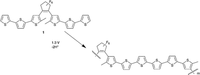 | ||
| Scheme 1 Electropolymerisation of 1 | ||
The polymer formed shows excellent redox behaviour with the polaronic and bipolaronic states formed at 0.8 V and 1.2 V vs. SCE, respectively.9 Importantly the changes in the UV/Vis-NIR absorption spectrum upon successive changes in oxidation state, in principle, allows for selective enhancement10 of the Raman scattering of the neutral and oxidised polymer. The resonance enhancement of the Raman spectrum was found to enable detection of the otherwise weak Raman signal above the Raman scattering of the PDMS walls of the microchannels.
Materials and methods
Device preparation
A kit for preparing poly(dimethylsiloxane) (PDMS) (Sylgard 184 (Dow Corning)) was obtained from Mavom BV (Alphen aan de Rijn, The Netherlands). PDMS on glass (Knittel glass) and PDMS on Indium Tin Oxide (ITO) devices were prepared using soft-lithography techniques.11 The channel network was made in PDMS by replication moulding. A PDMS prepolymer solution was cast onto a master consisting of a silicon wafer with a 100-μm-thick SU-8 photoresist layer patterned with the negative relief of the microchannel network. The silicon elastomer base and a curing agent were mixed in the ratio of 10![[thin space (1/6-em)]](https://www.rsc.org/images/entities/char_2009.gif) :1 (base:curing agent, w/w) and poured over the master, followed by standing for 30 min to allow air bubbles to escape from the layer. The PDMS microchannel layer was cured at 35 °C overnight. Holes were punched using a 1.5 or 3 mm biopt needle as inlets and outlets of the microchannel. Bonding to the glass or ITO surface was accomplished after 15 min of UV-ozone treatment of both surfaces and heating the assembly for further 30 min at 60 °C. Typical dimensions of the devices used were 100 μm × 100 μm × 2.5 cm.
:1 (base:curing agent, w/w) and poured over the master, followed by standing for 30 min to allow air bubbles to escape from the layer. The PDMS microchannel layer was cured at 35 °C overnight. Holes were punched using a 1.5 or 3 mm biopt needle as inlets and outlets of the microchannel. Bonding to the glass or ITO surface was accomplished after 15 min of UV-ozone treatment of both surfaces and heating the assembly for further 30 min at 60 °C. Typical dimensions of the devices used were 100 μm × 100 μm × 2.5 cm.
Patterned gold electrodes (200 nm with a 1 nm chromium interlayer) on glass were prepared via vacuum deposition using a home built system. The thickness of the Au layer formed by evaporation from a 99.99% gold crystal (SCHÖNE EDELMETAAL B.V) was controlled by a quartz crystal microbalance (Intellevation LTD). Prior to gold evaporation the glass microscope slides (Knittel Glass) were rinsed with 10% hydrochloric acid, water, acetone and ethanol. The slides were then subjected to air plasma cleaning for 1 min. The gold working electrode in the microfluidic channel was contacted to the potentiostat using a platinum wire secured with Scotch™ tape. The platinum wire counter electrode was introduced at the inlet of the channel and the pseudo-reference electrode, an Ag/AgCl wire, was introduced at the outlet of the channel (Fig. 1).
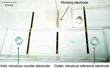 | ||
| Fig. 1 Microfluidic chip with gold electrodes used for electropolymerisation. | ||
Prior to polymerisation, the surface of the gold electrode in the microfluidic channel was cleaned electrochemically by cycling between −0.2 and 1.4 V vs. SCE in 0.5 M H2SO4. The cyclic voltammogram obtained shows the reconstruction of the gold (Fig. 2) with the gold oxide reduction becoming better defined with each cycle. It should be noted that for electrochemical applications it is necessary that freshly prepared microchannels are used and that the batch of PDMS used was cured within several days prior to microchannel construction.
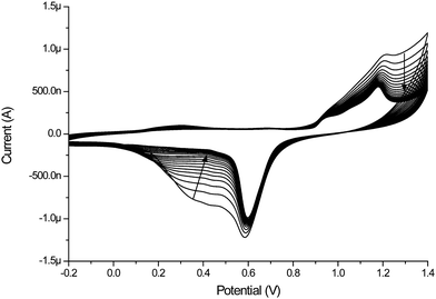 | ||
| Fig. 2 Electrochemical reconstruction of a gold electrode inside microfluidic channel, 0.5 M H2SO4, Pt-wire counter electrode, Hg/HgSO4 reference electrode, scan rate 0.5 V s−1. | ||
Electropolymerisation
2-(4-(3,3,4,4,5,5-Hexafluoro-2-(2-methyl-5-(5-(thiophen-2-yl)thiophen-2-yl)thiophen-3-yl)cyclopent-1-enyl)-5-methylthiophen-2-yl)-5-(thiophen-2-yl)thiophene (1)9 and the phenyl capped model compound 212 were available from earlier studies. Polymerisation of 1 (1.5 mM in CH2Cl2 with 0.1 M TBAPF6) was performed either potentiostatically at 1.3 V, or by repetitious cyclic voltammetry (−0.2 to 1.4 V vs. SCE). Electrochemical measurements were carried out using a CHInstruments 600C or 760C (bi)potentiostat. All potentials are quoted with respect to the SCE. Electrode areas were calculated by integration of the gold oxide reduction wave in 0.1 M H2SO4 (aq) prior to electropolymerisation of 1. Current densities are reported ±10%.After oxidative cleaning of the gold electrodes, the channel was flushed with water and filled with the monomer solution (a saturated solution of 1 in CH3CN with 0.1M TBAPF6). Electropolymerisation inside the microchannel was carried out potentiostatically. Prior to further analysis the channel was flushed with CH3CN and then with air.
Resonance Raman spectroscopy and spectroelectrochemistry
Raman spectra were recorded at λexc 632.8 nm and at 532 nm using a homebuilt Raman microscope based on an Olympus BX51 microscope fibre coupled to a HeNe laser (17 mW, Thorlabs) or DPSS CW laser (25 mW, Cobolt lasers), respectively, and an Andor idus DU-420-CCD detector (spectral calibration with acetonitrile:toluene, 1:1 v/v). Raman spectra at λexc 488 nm (Andor laser combiner, 50 mW, Andor) were obtained using a modified Andor revolution inverted microscope system coupled to a Shamrock 303i spectrograph and a Newton BU970 EMCCD (spectra calibrated with polystyrene). A Perkin Elmer Raman station/microscope was used to record spectra at λexc 785 nm (300 mW DPSS laser, Perkin Elmer). All laser sources were non-polarised at sample. For Raman spectroelectrochemistry a gold bead working electrode was employed (formed by melting gold wire using a hydrogen flame). The bead was cleaned electrochemically by oxidation in 0.5 M H2SO4 (aq) and subsequent stripping in 0.1 M HCl (aq) followed by cycling between −0.4 to 1.2 V vs. Hg/HgSO4 in 0.5 M H2SO4 (aq) for 20 cycles. Raman spectra are solvent subtracted and baseline corrected unless noted otherwise. Sample degradation due to absorption of laser excitation light can, under conditions where heat dissipation is insufficient, result in sample damage.13 Laser power at sample was adjusted where necessary to avoid sample damage. This was found to be especially of importance in analysis of modified surfaces within microfluidic channels. UV/Vis spectroelectrochemistry was carried out using a three electrode set-up in a 2 × 2 cm quartz cuvette holding an ITO working electrode (1 × 2.5 cm), Pt-wire counter electrode and Ag/AgCl pseudo reference electrode with CH3CN (0.1 M TBAPF6). A clean ITO slide was used as the blank. Spectra were recorded on an Analytik Jena Specord S600 diode array spectrometer.
Results and discussion
Electropolymerisation of 1
Polymerisation of monomer 1 was carried out as described ealier9 on Au, ITO and glassy carbon working electrodes. Although potentiostatic electropolymerisation could be achieved at potentials greater than 1.1 V (vs SCE), in general better quality films (as determined by subsequent cyclic voltammetry in monomer free solution) could be obtained by deposition by multi-cycle cyclic voltammetry. The thickness of the film is controlled through the number of cycles used for the deposition and good film adhesion was maintained even for relatively thick films (vide infra).The cyclic voltammogram of the polymer in monomer free solution shows two reversible oxidation waves at 0.85 and 1.15 V vs. SCE. Film thickness could be estimated from the current density of the first reductive wave with the examples of thin and thick films show in Fig. 3, the average thickness was found to be equivalent to a densely packed monolayer and several nm in thickness, respectively.14 However, it should be noted that for the thicker films it was apparent from optical microscopy that the surface coverage was not uniform (Fig. S3†).
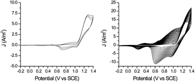 | ||
| Fig. 3 Electropolymerisation of 1 on gold bead electrodes a) thin film, 3 cycles, b) thick film 20 cycles (scan rate 0.1 V s−1, CH2Cl2, 0.1 M TBAPF6). | ||
The cyclic voltammetry of both thin and thick films in monomer free solution shows the expected redox waves for formation of the polaronic and bipolaronic states. In addition for both films a dip in current (indicated by a * in Fig. 4) was observed at low overpotentials that is characteristic of film discharging. This dip indicates that even for the relatively thin films complete reduction of the film does not occur. The incomplete reduction of the films is confirmed by resonance Raman spectroscopy (vide infra).
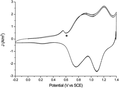 | ||
| Fig. 4 Cyclic voltammetry of a thin film (see Fig. 3) on an Au bead electrode in monomer free solution (CH2Cl2, 0.1 M TBAPF6, scan rate 0.5 V s−1). IR compensation (determined at 0.0 V) is employed. | ||
The scan rate dependence of the cyclic voltammetry of the films formed shows the expected linear dependence of current with scan rate at low scan rates and for thin films (Fig. 5). However it changes to a linear dependence on the square root of the scan rate for thick films at higher scan rates (Fig. 6). The change in scan rate dependence is indicative that charge diffusion in the film becomes rate limiting.
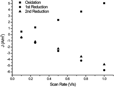 | ||
| Fig. 5 Scan rate dependence of the cyclic voltammetry of a thin film formed (Fig. 3a, Γ = 1.85 × 10⁻¹⁰ mol cm−2, where mol refers to moles of sexithiophene units) in monomer free solution. | ||
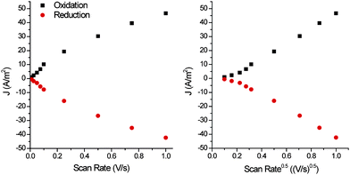 | ||
| Fig. 6 Scan rate dependence of the cyclic voltammetry of a thick film (Fig. 3b, Γ = 2.65 * 10−9 mol cm−2, where mol refers to moles of sexithiophene units) in monomer free solution. | ||
UV/Vis absorption spectroelectrochemistry
Deposition of an optically transmissive film on ITO allows for determination of the UV/Vis absorption spectra of the neutral, polaronic and bipolaronic states of the polymer film (Fig. 7).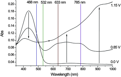 | ||
| Fig. 7 UV-Vis spectroelectrochemistry of the polymer deposited on an ITO electrode, 0.1 M TBAPF6 in CH3CN, Pt-wire counter electrode and Ag/AgCl wire reference electrode. The initially neutral polymer is oxidized first to the polaronic state (0.85 V) and then to the bipolaronic state (1.15 V), changes upon increase in oxidation potential are indicated by arrows. The wavelengths used to obtain resonance Raman spectra are indicated on by coloured lines. | ||
In the neutral state the polymer shows a maximum absorbance at 435 nm (Fig. 7).9 At 0.85 V the polaronic state is manifested in the appearance of a broad absorption at 700 nm and a decrease in the absorption at 435 nm. Increasing the potential to 1.15 V accesses the bipolaronic state with a further decrease in the absorption at 435 nm and an increase over the entire NIR region in agreement with spectral changes reported for mono- and dications of sexithiophenes.15
Resonance Raman spectroscopy
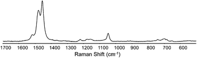
Resonance enhancement of Raman scattering can be achieved by exciting at or near an optical absorption band.10 The Raman spectrum of the neutral polymer film on ITO was recorded at λexc 488 nm (Fig. 8) and 532 nm (Fig. S7†). Three characteristic bands are observed at 1045, 1455 and 1480 cm−1. The band at 1045 cm−1 can be assigned to the Cβ–H bending, the bands at 1455 and 1480 cm−1 arise from the C![[double bond, length as m-dash]](https://www.rsc.org/images/entities/char_e001.gif) C symmetric and antisymmetric stretching modes of the thiophene backbone.15,16 However other known vibrations are not observed when analysing the polymer at this wavelength, such as the bands around 700 cm−1 where the Cα–S–Cα symmetric deformation is expected.17
C symmetric and antisymmetric stretching modes of the thiophene backbone.15,16 However other known vibrations are not observed when analysing the polymer at this wavelength, such as the bands around 700 cm−1 where the Cα–S–Cα symmetric deformation is expected.17
The neutral polymer does not absorb significantly at wavelengths >600 nm. Hence, excitation at 633 and 785 nm allows for selective probing of mono- and dicationic states with little or no contribution from the neutral polymer due to the strong absorption at these wavelengths observed for both species. Raman spectroelectrochemistry of a polymer film on a gold bead electrode at both wavelengths is shown in Fig. 9 and Fig. S6.†
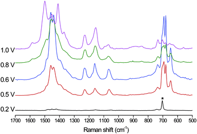 | ||
| Fig. 9 Resonance Raman spectra of the polymer on a gold bead electrode between 0.2 and 1.0 V. λexc 785 nm (Pt wire counter and Ag/AgCl reference electrodes) in CH2Cl2 (0.1 M TBAPF6) Spectra are normalized to solvent signal denoted by an asterisks and the potentials are with respect to the SCE. | ||
Raman spectra were recorded at several wavelengths, to demonstrate the bands observed were largely independent of the laser wavelength, but the signal intensity is dictated by the degree of resonance enhancement (Fig. S6 and Fig. S7†).18
Although the Raman spectrum of the neutral polymer film on a gold bead electrode is too weak to be observed at λexc 785 nm, oxidation of the polymer film at 0.85 and 1.15 V resulted in the appearance of strong Raman signals.
At 0.2 V, only vibrational modes of the solvent, dichloromethane, are observed. When the potential is increased to 0.5 V the monopolaron of the polymer is formed with bands at 1460, 1440, 1230, 1155, 1060, 690 and 680 cm−1. Oxidation at higher potentials results in the appearance of new bands at 1490 and 1415 cm−1 assigned to the dicationic state of the sexithiophene backbone. The lines at 690 and 680 cm−1 decrease in intensity at higher potentials as more of the bipolaronic state is formed. Subsequent reduction at 0.2 V leads to a complete disappearance of these bands. The pure spectra of the polaronic and bipolaronic species were obtained by scaled subtractions of the spectra (Fig. 9) at different potentials (Fig. 10). The spectrum of the monopolaron is essentially the same as that of the monocation of the model compound 2 (Fig. S4†). Similar spectral changes are observed at 532 and 632.8 nm, but with different relative intensity between the bands of each species (see Fig. S6 and Fig. S8†).
 | ||
| Fig. 10 Resonance Raman spectra of mono (lower) and bipolaronic state (upper) of the polymer on a gold working electrode (obtained by subtraction, see text for details) at λexc 785 nm. | ||
At 633 nm the polaronic and bipolaronic states are resonantly enhanced, however at 532 nm all three states (neutral, polaron and bipolaron) are expected to be resonantly enhanced. To demonstrate this Raman spectroelectrochemistry was carried out at λexc 532 nm. The dry polymer showed signals corresponding to the spectrum obtained at λexc 488 nm. When the polymer film is in contact with electrolyte solution strong fluorescence relative to the Raman scattering was observed. Upon doping the film the fluorescence intensity decreased and Raman spectra of the polaron and bipolaron could be obtained (Fig. S8†).
When a thicker polymer film is analysed directly after polymerisation a mixture of bands of the mono- and bipolaronic species are observed in the Raman spectra recorded at 785 nm.
Dependence of charge trapping in the polymer film on film thickness
As noted above, as the polymer film becomes thicker the full neutralisation of the polymer becomes increasingly difficult due to the more rapid reduction of polarons near the electrode, which creates an insulating region preventing full reduction. In situ resonance Raman spectroelectrochemistry was employed to monitor this effect in real time as the film is being deposited by cyclic voltammetry. The cyclic voltammogram is shown in Fig. 11 together with Raman spectra recorded in real time at 1.0 V and 0.1 V (Fig. 12 and Fig. 13).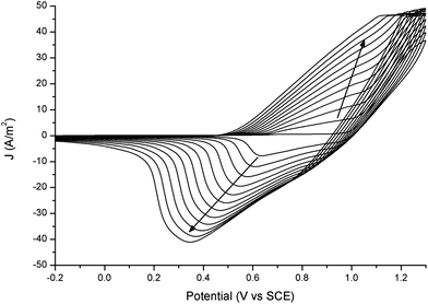 | ||
| Fig. 11 Electropolymerisation on a gold bead electrode followed with Raman spectroscopy (see fig. 12 and 13) (scan rate 0.1 V s−1), 1 mM 1 in CH2Cl2 (0.1M TBAPF6). | ||
 | ||
| Fig. 12 Polymerisation followed with Raman at λexc 785 nm in situ on a gold-bead, spectra taken during cyclic voltammetry, during the section of the cycle from 1.0 V to 1.3 V and back to 1.0 V; Raman spectra are 3 accumulations of 2 s each. The asterisk denotes solvent band. | ||
 | ||
| Fig. 13 Polymerisation followed with Raman at λexc 785 nm in situ on a gold-bead, spectra taken during cyclic voltammetry, during the section of the cycle from 0.1 V to −0.2 V and back to 0.1 V; Raman spectra are 3 accumulations of 2 s each. Asterisk denotes solvent band. | ||
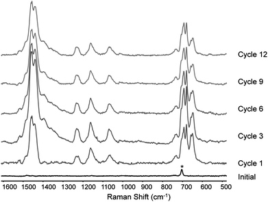
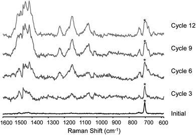
At high potentials (ca. 1.0 V), the Raman spectra of, primarily, the polaronic state is observed after the first cycle and increases in intensity with cycle number for the first few cycles (Fig. 12). At low potentials (0.1 V), the Raman scattering of the polaronic state is weak for the first six cycles however thereafter the Raman signal of the oxidised polymer increases in intensity (Fig. 13). The persistence of signals due to the polaronic state when the potential is returned to 0.1 V after more than six cycles is ascribed to trapping of charges at the outer layers of the polymer film upon neutralisation (and hence loss of conductivity) of the inner layers of the film.
Microfluidic channel surface modification
The solubility of monomer 1 in CH3CN is limited, however solvents in which it is more soluble are less compatible with the material (PDMS) used to form the microchannels employed in the present study.19 Nevertheless, despite the lower concentration of monomer 1 in CH3CN (<0.5 mM), electropolymerisation could be achieved within the channel potentiostatically.20 After polymerisation the channel was rinsed with CH3CN and emptied to remove excess monomer and electrolyte prior to analysis.Examination of the channel by optical microscopy after electropolymerisation of 1 allowed for observation of the charging and discharging of the polymer film charges during cyclic voltammetry, manifested as a colour change from orange to green, and then to orange upon re-reduction (Fig. 14).
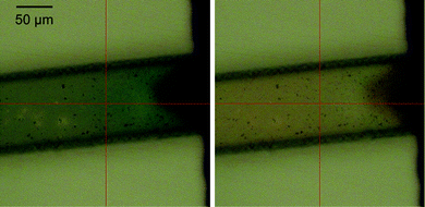 | ||
| Fig. 14 Colour change of the polymer film in a microfluidic channel. Polymer at oxidative potential (1.0 V) turns green (right) and returns to slightly orange once reduced back (left). | ||
Resonance Raman spectroscopy was used to analyse the polymer modified electrodes inside the microchannels. Direct microRaman analysis of the polymer film while undergoing oxidation and reduction within the channel was not practical due to rapid heating and evaporation of the solvent. Nevertheless non-destructive in situ microRaman analysis of the polymer modified electrodes within the microchannels was possible after the channel was drained of solvent enabling identification of the presence of polarons and bipolarons in the polymer film.
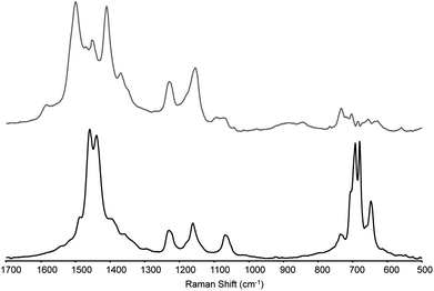
The resonance Raman spectra of a relatively thick polymer film on a glassy carbon electrode and a gold electrode within the microchannel after potentiostatic deposition of the polymer, washing with monomer free solution and draining of the solvent, correspond well (Fig. 15). The incomplete reduction of the polymer films results in the observation of resonantly enhanced spectra in which a mixture of the mono- and bipolarons are observed. The Raman spectrum in both cases indicate that the film contains polarons and bipolarons (trapped charges). Application of a potential of 1.0 V to a polymer modified electrode within the microchannel, after which the channel is emptied and rinsed to remove electrolyte solution, results in an increase in the intensity of the polaronic and bipolaronic Raman signals as expected for an increased oxidation state.
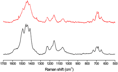 | ||
| Fig. 15 Resonance Raman spectra at λexc 785 nm of polymer on a gold electrode in a microfluidic channel (upper) and on 3 mm glassy carbon electrode (lower), both are (dry) deposited polymers, resonance enhanced signals arise due to incomplete reduction of the polymer film. At 785 nm only polarons and bipolarons are observed as the Raman spectrum of neutral polymer is not resonantly enhanced at this wavelength. | ||
To verify that the electropolymerisation occurred only at the working electrode within the microchannel, a microfluidic channel with several gold electrodes was used, in which only one electrode was connected to the potentiostat. The formation of polymer occurred only on the electrode contacted (as determined by optical microscope and resonance Raman spectroscopy, Fig. S10†).
Conclusions
Here we demonstrate the successful modification of surfaces inside a microfluidic channel by electropolymerisation. A major challenge however is the subsequent characterisation of the modified surfaces. We have shown that resonance Raman spectroscopy is an effective tool in achieving the levels of sensitivity required to detect the oxidation state of the polymer films in situ albeit without solvent present within the channels during analysis. In the oxidised states the sexithiophene polymer shows strong resonance enhancement enabling application of Raman spectroscopy as a non-invasive technique to characterise thin polymer films deposited on Au electrodes within microfluidic devices. Importantly the analysis does not require destruction (opening) of the channel.Acknowledgements
The authors thank Oleksii Ivashenko for assistance with evaporation of gold and The Netherlands Organisation for Scientific Research NWO Vidi (HL, WRB) and NanoNed for financial support.Notes and references
- H. Kuhn, Thin Solid Films, 1983, 99, 1–16 CrossRef CAS; T. P. Russell, Science, 2002, 297, 964–967 CrossRef; J. Robertus, W. R. Browne and B. L. Feringa, Chem. Soc. Rev., 2010, 39, 354–378 RSC.
- Y. Liu, L. Mu, B. Liu and J. Kong, Chem.–Eur. J., 2005, 11, 2622–2631 CrossRef CAS.
- I. Wong and C. Ho, Microfluid. Nanofluid., 2009, 7, 291–306 CrossRef CAS; H. Logtenberg, M. J. Lopez-Martinez, B. L. Feringa, E. Verpoorte and W. R. Browne, Lab Chip, 2011, 11, 2030–2034 RSC.
- Y. Lu, G. Shen, C. Zhao and S. Guo, Electrochim. Acta, 2009, 54, 4253–4257 CrossRef CAS.
- J. Wang, Y. L. Bunimovich, G. Sui, S. Savvas, J. Wang, Y. Guo, J. R. Heath and H. Tseng, Chem. Commun., 2006, 3075–3077 RSC.
- T. A. Skotheim and J. R. Reynolds, Conjugated Polymers, CRC Press, 2007 Search PubMed.
- G. Shi, J. Xu and M. Fu, J. Phys. Chem. B, 2002, 106, 288–292 CrossRef CAS.
- H. T. Baytekin, T. Wirth, T. Gross, M. Sahre, W. E. S. Unger, J. Theisen and M. Schmidt, Surf. Interface Anal., 2010, 42, 1417–1431 CrossRef CAS.
- J. Areephong, T. Kudernac, J. J. D de Jong, G. T. Carroll, D. Pantorott, J. Hjelm, W. R. Browne and B. L. Feringa, J. Am. Chem. Soc., 2008, 130, 12850–12851 CrossRef CAS.
- D. P. Strommen and K. Nakamoto, J. Chem. Educ., 1977, 54, 474–478 CrossRef CAS.
- J. C. McDonald, D. C. Duffy, J. R. Anderson, D. T. Chiu, H. Wu and O. J. A. Schueller, Electrophoresis, 2000, 21, 27–40 CrossRef CAS; J. C. McDonald and G. M. Whitesides, Acc. Chem. Res., 35, 491–499 CrossRef.
- J. Areephong, J. H. Hurenkamp, M. T. W. Milder, A. Meetsma, J. L. Herek, W. R. Browne and B. L. Feringa, Org. Lett., 2009, 11, 721 CrossRef CAS; M. T. W. Milder, J. Areephong, B. L. Feringa, W. R. Browne and J. L. Herek, Chem. Phys. Lett., 2009, 479, 137 CrossRef.
- J. E. Pereira da Silva, M. L. A. Temperini and S. I. Cordoba de Torresi, Electrochim. Acta, 1999, 44, 1887 CrossRef CAS.
- Measurement of film thickness by elipsometry was impractical because the visible absorption spectrum of the film used in such an experiment could not be estimated accurately.
- T. M. Clarke, K. C. Gordon, P. Wagner and D. L. Officer, J. Phys. Chem. A, 2007, 111, 2385–2397 CrossRef CAS.
- M. Akimoto, Y. Furukawa, H. Takeuchi, I. Harada, Y. Soma and M. Soma, Synth. Met., 1986, 15, 353–360 CrossRef CAS.
- G. Louarn, J. P. Buisson, S. Lefrant and D. Fichou, J. Phys. Chem., 1995, 99, 11399–11404 CrossRef CAS.
- Furthermore although overall the differences are caused by the difference in absorption at different wavelengths, the intensity pattern in the resonance Raman spectrum of each species is also wavelength dependent. Specifically it depends on the electronic nature of the optical transition being excited into. Hence a priori differences in intensity of the Raman spectra at different excitation wavelengths cannot be directly related with the concentrations of each species present.
- J. N. Lee, C. Park and G. M. Whitesides, Anal. Chem., 2003, 75, 6544–6554 CrossRef CAS.
- Electropolymerisation was not noticeably affected by the fabrication method used to prepare the microchannel, i.e. channels bonded using UV-O3 or air-plasma were equivalent.
Footnote |
| † Electronic supplementary information (ESI) available: Additional Raman spectra and pictures of devices used. See DOI: 10.1039/c1ay05475a |
| This journal is © The Royal Society of Chemistry 2012 |