Automated sub-100 nm local anodic oxidation (LAO)-directed nanopatterning of organic monolayer-modified silicon surfaces†
Bruno
Fabre
* and
Cyril
Herrier
UMR 6226 CNRS/Université de Rennes, Sciences Chimiques de Rennes, Matière Condensée et Systèmes Electroactifs (MaCSE), Campus de Beaulieu, 35042, Rennes, France. E-mail: bruno.fabre@univ-rennes1.fr; Fax: +33 (0) 2 2323 6732; Tel: +33 (0) 2 2323 6550
First published on 3rd November 2011
Abstract
The fabrication of silicon oxide nanopatterns using the local anodic oxidation (LAO) by a conducting AFM tip of different organic monolayer (decyl, dodecyl, hexadecyl and undecanoic acid)-modified Si(111) surfaces is reported. It is demonstrated that the threshold bias voltage of oxide formation increases with the monolayer thickness and decreases when acid end groups are used instead of methyl. The automatization of the LAO process has allowed the perfect replication of vectorized complex drawings (e.g. compass card and longship) on silicon using the undecanoic acid monolayer as the model molecular resist. Under optimized experimental conditions (namely, bias voltage of 8 V applied to the surface and writing rate of 1 μm s−1), highly reproducible and uniform 2–3 nm thick oxide patterns have been electrogenerated with a minimum lateral resolution of 80 nm. Interestingly, the silicon oxide nanopatterns have been selectively dissolved in diluted hydrogen fluoride solution to generate potentially reactive hydrogenated areas. These hydrogenated sites have then been used for the electroless deposition of gold nanoparticles by galvanic displacement. This approach was found to be convenient and fast to metallize the patterns initially produced by LAO. The average diameter of deposited gold particles decreased from 20 to 2 nm with decreasing the gold salt concentration from 100 to 1 μM.
1. Introduction
Scanning probe microscopy (SPM)-based techniques, i.e. scanning tunneling microscopy (STM), atomic force microscopy (AFM) and near-field scanning optical microscopy (NSOM), have been demonstrated to be powerful and reliable lithographic methods for the fabrication of functional micro- and nanostructures on surfaces with high control on both their composition and spatial resolution.1–4 The patterning of surfaces using SPM can be categorized into four principal modes: the mechanical scribing of the surface using a hard probe tip,5,6 the dip-pen nanolithography using a tip coated with a molecular “ink”,7,8,9 the electrochemical patterning using a conducting tip10,11 and the optical lithography using a transparent tip as a waveguide.3,12 These have been successfully used for the controlled positioning or the fabrication of nanometre-sized structures on different types of substrates, semiconducting, metallic and carbon-based surfaces. Among the electrochemically directed lithographic methods, the local anodic oxidation (LAO) of oxygen-free hydrogen-terminated silicon (H–Si)13–23 and self-assembled organic monolayers on H–Si,24–30 oxidized silicon31–39 and gold40 surfaces resulted in both the desorption of the monolayer and the growth of silicon oxide when high bias voltages were applied. For lower voltages, it has been demonstrated that this process led to the conversion of the end groups of the monolayer into carboxyl moieties28,31–32,39 or to the cleavage of bonds in the organic chains.41,42 Compared with unmodified H–Si, the organic monolayer covalently bound to H–Si played the role of the molecular resist enabling the formation of well-defined patterns on the surface and also preventing the oxidation process from propagating around the patterned region during and after the LAO step. Therefore, the densest possible packing of the monolayer is sought in order to provide an efficient passivating and insulating environment. There are several advantages to this convenient and flexible lithographic approach involving monolayer-modified silicon surfaces. For some applications, it may be convenient to keep the electrogenerated oxide patterns intact or to react them with some organosilane derivatives (trialkoxy- and trichlorosilanes) in order to introduce patterned assemblies of functional molecules to silicon. Furthermore, one may also take advantage of the fact that the oxide features electrogenerated on silicon are easily removed by exposure to aqueous solutions of HF while the unexposed surrounding monolayer is inert,43 provided that it is attached to the silicon surface through Si–C interfacial bonds. Thus, the newly hydrogen-terminated areas can react with substituted 1-alkenes and 1-alkynes to yield ω-functionalized monolayers through a hydrosilylation route.44–46 However, the development of such functional patterned interfaces requires as a prerequisite that the process of tip-induced surface oxidation is optimized and well-mastered in order to electrogenerate uniform and spatially resolved patterns with high reproducibility.Herein, we discuss the effects of key experimental factors (namely bias voltage and oxidation rate) as well as the grafted monolayer (chain length and nature of the end group) on the formed oxide topography. Moreover, we also present an automated LAO platform devoted to the writing of nanopatterns with complicated geometrical shapes on modified silicon surfaces using undecanoic acid monolayer as the model molecular resist. Compared with previously reported examples focusing on LAO of modified silicon surfaces, our approach enables the fabrication of nanopatterns with a much higher level of complexity. The nanopatterned surfaces were then used for the selective deposition of gold nanoparticles.
2. Experimental
2.1. Reagents
Acetone (MOS electronic grade, Erbatron from Carlo Erba), anhydrous ethanol (RSE electronic grade, Erbatron from Carlo Erba), acetic acid (99.7%, Acros) and trichloroethylene (VLSI electronic grade from Carlo Erba) were used without further purification. Dichloromethane (min. 99.5%, AnalaR Normapur from VWR) from SDS was distilled over phosphorus pentoxide (Sicapent from Merck) before use.The chemicals used for cleaning and etching of silicon wafer pieces (30% H2O2, 96–97% H2SO4, 40% NH4F and 50% HF solutions) were of VLSI semiconductor grade (Riedel-de-Haën). 1-Decene, 1-dodecene and 1-hexadecene (Fluka, 95%) were passed through a neutral, activated alumina column, then distilled over sodium and stored under argon in a fridge. Undecylenic acid (Aldrich, 98%) was passed through a neutral, activated alumina column prior to use to remove residual water and peroxides.
2.2. Preparation of the modified n-type Si(111) surfaces
All Teflon vials used for cleaning of silicon were previously decontaminated in 3![[thin space (1/6-em)]](https://www.rsc.org/images/entities/char_2009.gif) :1 v/v concentrated H2SO4/30% H2O2 at 100 °C for 30 min, followed by copious rinsing with ultra-pure water.
:1 v/v concentrated H2SO4/30% H2O2 at 100 °C for 30 min, followed by copious rinsing with ultra-pure water.
Caution: The concentrated H2SO4:H2O2 (aq) piranha solution is very dangerous, particularly in contact with organic materials, , and should be handled extremely carefully.
Single side polished silicon(111) samples (n-type, phosphorus doped, 5–10 Ω cm, thickness = 525 ± 25 μm, from Siltronix) were cut into 1.5 × 5.0 cm2 pieces from the same silicon wafer to ensure the maximum reproducibility of hydrogen-terminated and further molecular monolayer-modified surfaces. The sample was sonicated for 10 min successively in acetone, ethanol and ultra-pure 18.2 MΩ cm water (Elga Purelab Classic UV, Veolia Water STI). It was then cleaned in 3:1 v/v concentrated H2SO4/30% H2O2 at 100 °C for 30 min, followed by copious rinsing with ultra-pure water. The surface was etched with argon-deaerated ppb grade 40% aqueous NH4F for 15–20 min at room temperature to obtain atomically flat monohydride-terminated Si(111) (H–Si(111)).47 It was then dipped in argon-deaerated water for a few seconds, dried under an argon stream, and transferred immediately into a Pyrex Schlenk tube containing ca. 20 mL of neat alkene (namely, 1-decene, 1-dodecene, 1-hexadecene or undecylenic acid), previously deoxygenated at 100 °C for 1 h at least, then allowed to cool down to ca. 30–40 °C before introducing H–Si(111). After additional argon bubbling for 30 min, the Schlenk tube was thoroughly sealed and irradiated in a Rayonet photochemical reactor at 300 nm for 3 h. The alkyl monolayer-modified silicon surface was rinsed copiously with trichloroethylene and acetone, and dried under an argon stream. The undecanoic acid-modified surface was rinsed copiously with dichloromethane, then dipped in hot acetic acid (65 °C) for 2 × 20 min and dried under an argon stream. It has been demonstrated that the rinsing in hot acetic acid leaves the functionalized surface smooth and perfectly free of physisorbed contaminants.48
2.3. Deposition of gold nanoparticles on nanopatterned Si(111) surfaces
After the LAO experiments, the nanopatterned surfaces were dipped in aqueous HF 2% for 2 min to convert the oxide to hydrogenated areas and then dipped for a few seconds in an aqueous gold salt solution containing HF 0.25% and hydrogen tetrachloroaurate(III) hydrate HAuCl4 (Strem Chemicals) at 100, 10 or 1 μM. The surface was thoroughly rinsed with ultra-pure water and dried under an argon stream.2.4. Surface characterizations
2.5. Automated LAO-directed nanopatterning of monolayer-modified Si(111) surfaces
The simplified experimental setup to produce complex patterns from LAO using a conducting AFM tip is shown in Fig. S1 (Supporting Information).† The automated lithography requires a system of vectors describing the AFM tip motion. The first step consists in obtaining a numerical picture of the desired feature. Computer Assisted Drawing (CAD) software such as AutoCAD is powerful software for obtaining numerical drawings which are easily manipulated between different computers. The generated black and white image is then converted into a vector system using the Scan2CAD Computer Assisted Manufacture software (version 8 from Avia). The dxf (Drawing Exchange Format) file containing the vector coordinates is then read from the PicoLith lithography software (from Scientec) driving the multipurpose XYZ closed-loop scanner (see the movie in Supporting Information†). Interestingly, if desired, different lithography parameters such as the tip speed, the force setpoint and the voltage can be assigned to each vector. Compared with an open-loop scanner (that does not have sensors for closed-loop feedback correction), the closed-loop scanner can replicate perfectly the pattern drawn in the graphics interface (Fig. S2 in Supporting Information†). LAO experiments were performed in contact mode in ambient conditions at a controlled 50 ± 5% relative humidity. Humidity values lower than 35% and higher than 70% were found to lead to nonuniform and poorly reproducible silicon oxide patterns. During the LAO experiment, force setpoint was maintained at around 20 nN. After patterning, AFM imaging was performed in contact mode with the same tip.3. Results and discussion
Before performing LAO-directed nanopatterning experiments on modified Si(111) surfaces, it is a prerequisite to control both the quality, the compactness, and the cleanliness of the grafted organic monolayers because such characteristics could considerably affect the oxide growth process. First, static water contact angles of the prepared alkyl (i.e.decyl, dodecyl and hexadecyl) monolayer-modified Si(111) are relatively constant at 108° (Table S1 in Supporting Information†), in line with usually reported values for densely packed alkyl monolayers.49–51 In contrast, due to the hydrophilic character of the acid headgroup, the undecanoic acid-modified surface showed a lower contact angle of 45°, also in agreement with other reported data.52–54 The AFM images of all prepared monolayers show atomically flat, defect-free terraces of Si(111) with ca. 3 Å step heights corresponding to a silicon bilayer, and a root mean square (rms) roughness of approximately 1.5 Å, which is not significantly dependent on both the length of the alkyl chain and the nature of the headgroup (Fig. S3†). This topography is identical to that of H–Si(111)55,56 and other methyl-terminated57 or ω-functionalized alkyl monolayers.48,52,58–61 All these data clearly demonstrate that the prepared monolayers are smooth, dense and high-quality.Then, preliminary LAO experiments have been performed on these differently modified Si(111) surfaces in order to determine the optimum experimental conditions enabling the fabrication of spatially resolved silicon oxide patterns with high reproducibility. Toward this goal, the effects of several parameters have been studied, namely the bias voltage, the scan (i.e. writing) rate of the AFM tip and the nature of the grafted monolayer. First, the effects of the bias voltage are illustrated in Fig. 1 with the LAO-directed fabrication of oxide lines on dodecyl-modified Si(111). Fig. 1 shows AFM topography and lateral force microscopy images obtained at different bias voltages for a constant writing rate of 0.1 μm s−1. For low voltages (lower than 5 V), we observe a weakly negative friction contrast in the lines indicating a more hydrophilic character and barely detectable height changes in the AFM topography (smaller than 2 Å). In this range, carboxylic acid groups are formed upon the oxidation of the methyl end groups of the monolayer. Upon increasing the voltage (6 and 7 V), the monolayer degradation occurs simultaneously accompanied by the oxidation of the underlying silicon, as evidenced by an increase in both negative friction and positive height contrasts. At the highest voltages, the monolayer is completely degraded followed by the growth of silicon oxide lines. As already reported for H–Si20 and alkyl-modified Si,25,26 an inverse logarithmic dependence between the line height and the writing rate is observed (Fig. 2), consistent with a field-induced electrochemical process and limited by the charge migration through the oxide layer. The LAO process at high bias voltages can be divided into three stages:25,40 in the first stage, the oxidizing species, presumably hydroxide anions produced from the reduction of water at the AFM tip, oxidize the end groups of the monolayer, then they can penetrate into the alkyl monolayer to degrade the carbon chains, and reach the silicon substrate causing its oxidation (Fig. 1D).
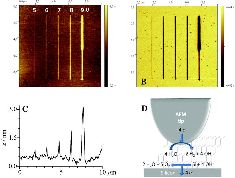 | ||
| Fig. 1 AFM topography (A) and friction (B) images of silicon oxide lines electrogenerated on dodecyl monolayer-modified Si(111) at different voltage values (5 to 9 V) and for a constant writing rate (0.1 μm s−1). (C) Corresponding cross-section profile taken in the middle of the image. (D) Mechanism of oxide growth on monolayer-modified silicon surface. Relative humidity is 50 ± 5%. Potential is applied to the sample and the tip is grounded. | ||
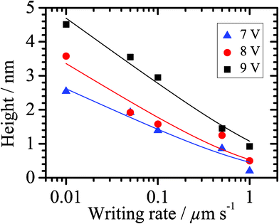 | ||
| Fig. 2 Oxide height vs. writing rate plots for different sample bias voltages applied on a dodecyl-modified Si(111) surface. The solid lines correspond to the data fitted curves using a logarithmic function. | ||
Similar oxide lines can be electrogenerated on the other modified surfaces and representative data are reported in Fig. 3. A linear dependence between the line height and the voltage is observed for all the prepared alkyl monolayers. Furthermore, a similar slope is obtained which indicates that there is no significant effect of the monolayer thickness on the growth kinetics. In contrast, the threshold bias voltage of oxide formation increases with the monolayer thickness. This threshold bias voltage is also decreased when acid end groups are used instead of methyl (compare undecanoic acid against dodecyl monolayers) which can be explained by a better stabilization of the water meniscus owing to the hydrophilic character of the acid monolayer.
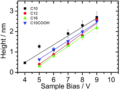 | ||
| Fig. 3 Mean oxide height vs. sample bias voltage plots as a function of the nature of the organic monolayer covalently bound to Si(111). The silicon oxide patterns were electrogenerated by LAO using a writing speed of 0.1 μm s−1. | ||
From these preliminary experiments, it has been thus deduced that a bias voltage of 8 V applied on undecanoic acid-modified Si(111) and a writing rate of 1 μm s−1 are appropriate LAO parameters for the automated fabrication of complex and spatially resolved silicon oxide patterns with high reproducibility and an appreciable rate. Under these conditions, it has been possible to electrogenerate various complex features as those shown in Fig. 4. These 2–3 nm thick oxide patterns have been drawn in about 15–20 min and the minimum lateral resolution that can be reached is ca. 80 nm.
 | ||
| Fig. 4 AFM images and corresponding cross-section profiles (taken in the middle of the images) of oxide compass card and longship drawings electrogenerated using automated LAO of undecanoic acid-modified Si(111) surfaces (applied sample bias of 8 V, writing rate of 1 μm s−1) before (left side) and after (right side) etching in aq HF 2% for 2 min. | ||
As already demonstrated for photochemically micropatterned silicon surfaces,62,63 an interest of this electrochemical lithography method is that the silicon oxide patterns can be selectively dissolved in diluted hydrogen fluoride solution to generate potentially reactive hydrogenated areas. The AFM analysis demonstrates that the oxidized areas have been converted to 2–3 nm deep hydrogenated channels after etching in HF for 2 min and correct positioning of the AFM tip on top of the patterned area (Fig. 4).
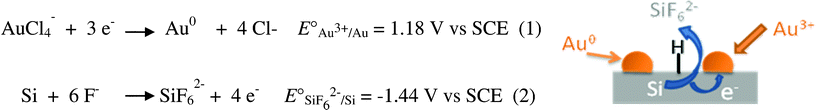
As an example of spatially localized functionalization, we have used the hydrogenated patterns for the selective deposition of metallic nanoparticles like gold using the electroless deposition by galvanic displacement.64–68 If we refer to the redox potentials of the Au3+/Au and SiF62−/Si redox couples (Scheme 1), the spontaneous oxidation of silicon into soluble hexafluoride silicon salt is expected in the presence of gold(III) salt and hydrogen fluoride. The semiconductor acts as a source of electrons that reduce the gold(III) salt to metallic gold on the surface and hydrogen fluoride is required to ensure continuous metallic growth. Using a HF concentration of 0.25% and a gold salt concentration of 100 μM, we obtain after only 5 s a high density of gold nanoparticles in the patterns (Fig. 5). The average diameter of these particles is found to be 20 ± 5 nm. However, the electrochemical reduction of metal salt at the remaining H–Si sites, after diffusion through pinholes and defects of the resist monolayer, is certainly responsible for the presence of nanoparticles around the patterns. Changing the metal concentration results in the significant improvement of the deposition selectivity. A gold salt concentration of 10 μM leads to a continuous deposition of nanoparticles inside the channels with an average diameter of 5 nm and only some nanoparticles around the patterns are observed. For the most diluted solution (1 μM), we observe a discontinuous deposition of 2 nm diameter nanoparticles inside the channels and almost no particles around the patterns.
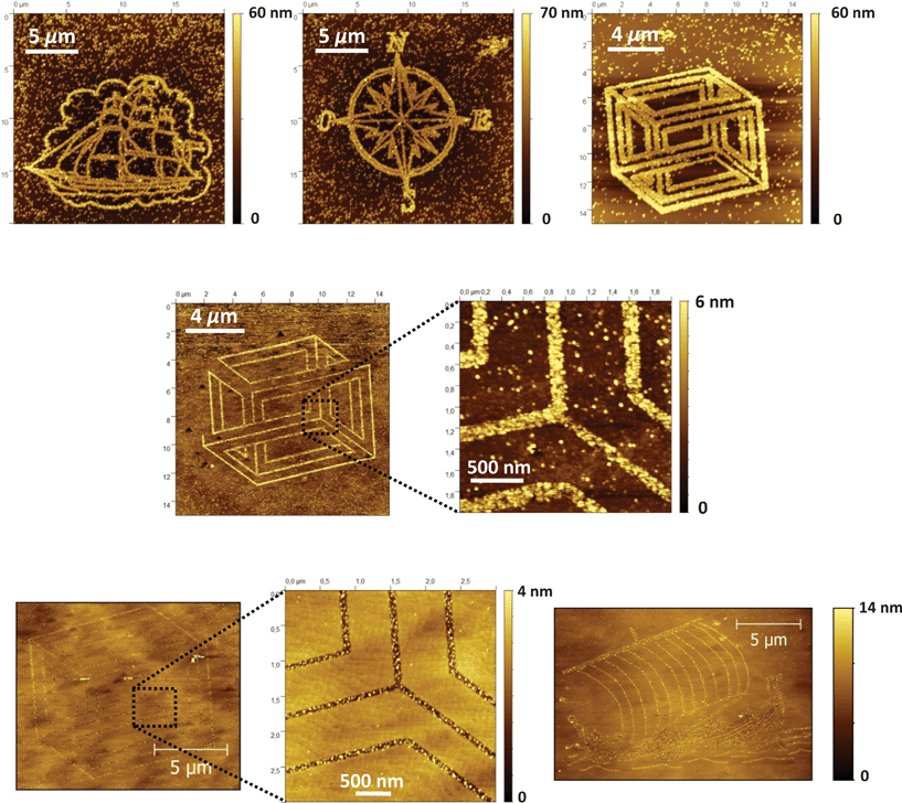 | ||
| Fig. 5 AFM images of gold nanoparticles deposited on nanopatterned undecanoic acid-modified Si(111) after etching in HF 2% for 2 min and dipping for 5 s in a gold salt solution containing HF 0.25% and HAuCl4 at 100 (top), 10 (middle) or 1 μM (bottom). | ||
 | ||
| Scheme 1 Deposition of gold nanoparticles on silicon surfaces by galvanic displacement. | ||
4. Conclusion
In conclusion, we have demonstrated that the automated local anodic oxidation is a flexible, efficient and precise method for nanopatterning molecular resist-modified silicon surfaces in ambient conditions with sub-100 nm complex drawn features. Interestingly, the electrogenerated patterns could be further functionalized using common silicon surface reactions such as the silanization and hydrosilylation methods. In this work, the hydrogenated nanopatterns have been used for the self-directed electroless deposition of gold nanoparticles and this reaction resulted in the formation of gold–silicon intermetallics. However, gold deposition was also observed in the unpatterned areas to a much lesser extent as a result of the presence of some H–Si sites remaining after the grafting step of the organic monolayer. It is very likely that the deposition selectivity could be improved by using either alkyne-derived monolayers as molecular resists which show a higher surface coverage than alkene-derived monolayers or metal salts with lower oxidation potentials, like Pt or Ag, in order to reduce the driving force for galvanic displacement. Such interfaces could be of interest for the fabrication of metallic interconnects and electrode networks but also for the controlled cell adhesion and growth.Acknowledgements
This work was financially supported by CNRS, UMR 6226 CNRS/Université de Rennes 1 and Agence Nationale de la Recherche (ANR-07-BLAN-0170-02, Project “CLUSTSURF”). C.H. acknowledges “Région Bretagne” for a PhD grant.References
- D. Wouters and U. S. Schubert, Nanolithography and Nanochemistry: Probe-Related Patterning Techniques and Chemical Modification for Nanometer-Sized Devices, Angew. Chem., Int. Ed., 2004, 43, 2480–2495 CrossRef CAS.
- S. Krämer, R. R. Fuierer and C. B. Gorman, Scanning Probe Lithography Using Self-Assembled Monolayers, Chem. Rev., 2003, 103, 4367–4418 CrossRef.
- R. M. Nyffenegger and R. M. Penner, Nanometer-Scale Surface Modification Using the Scanning Probe Microscope: Progress since 1991, Chem. Rev., 1997, 97, 1195–1230 CrossRef CAS.
- R. Garcia, R. V. Martinez and J. Martinez, Nano-Chemistry and Scanning Probe Nanolithographies, Chem. Soc. Rev., 2006, 35, 29–38 RSC.
- L. Yang, Y.-Y. Lua, M. V. Lee and M. R. Linford, Chemomechanical Functionalization and Patterning of Silicon, Acc. Chem. Res., 2005, 38, 933–942 CrossRef CAS.
- R. W. Carpick and M. Salmeron, Scratching the Surface: Fundamental Investigations of Tribology with Atomic Force Microscopy, Chem. Rev., 1997, 97, 1163–1194 CrossRef CAS.
- R. D. Piner, J. Zhu, F. Xu, S. Hong and C. A. Mirkin, “Dip-Pen” Nanolithography, Science, 1999, 283, 661–663 CrossRef CAS.
- D. S. Ginger, H. Zhang and C. A. Mirkin, The Evolution of Dip-Pen Nanolithography, Angew. Chem., Int. Ed., 2004, 43, 30–45 CrossRef.
- B. Basnar and I. Willner, Dip-Pen-Nanolithographic Patterning of Metallic, Semiconductor, and Metal Oxide Nanostructures on Surfaces, Small, 2009, 5, 28–44 CrossRef CAS.
- D. Wouters, S. Hoeppener and U. S. Schubert, Local Probe Oxidation of Self-Assembled Monolayers: Templates for the Assembly of Functional Nanostructures, Angew. Chem., Int. Ed., 2009, 48, 1732–1739 CrossRef CAS.
- F. C. Simeone, C. Albonetti and M. Cavallini, Progress in Micro- and Nanopatterning via Electrochemical Lithography, J. Phys. Chem. C, 2009, 113, 18987–18994 CAS.
- R. C. Dunn, Near-Field Scanning Optical Microscopy, Chem. Rev., 1999, 99, 2891–2928 CrossRef CAS.
- J. A. Dagata, J. Schneir, H. H. Harary, C. J. Evans, M. T. Postek and J. Bennett, Modification of Hydrogen-Passivated Silicon by a Scanning Tunneling Microscope Operating in Air, Appl. Phys. Lett., 1990, 56, 2001–2003 CrossRef CAS.
- J. A. Dagata, Device Fabrication by Scanned Probe Oxidation, Science, 1995, 270, 1625–1626 CrossRef CAS.
- H. C. Day and D. R. Allee, Selective Area Oxidation of Silicon with a Scanning Force Microscope, Appl. Phys. Lett., 1993, 62, 2691–2693 CrossRef CAS.
- N. Barniol, F. Perez-Murano and X. Aymerich, Modification of HF-Treated Silicon (100) Surfaces by Scanning Tunneling Microscopy in Air under Imaging Conditions, Appl. Phys. Lett., 1992, 61, 462–464 CrossRef CAS.
- L. Tsau, D. Wang and K. L. Wang, Nanometer Scale Patterning of Silicon (100) Surfaces by an Atomic Force Microscope Operating in Air, Appl. Phys. Lett., 1994, 64, 2133–2135 CrossRef CAS.
- P. Fay, R. T. Brockenbrough, G. Abeln, P. Scott, S. Agarwala, I. Adesida and J. W. Lyding, Scanning Tunneling Microscope Stimulated Oxidation of Silicon (100) Surfaces, J. Appl. Phys., 1994, 75, 7545–7549 CrossRef CAS.
- T. Teuschler, K. Mahr, S. Miyazaki, M. Hundhausen and L. Ley, Nanometer-Scale Field-Induced Oxidation of Si(111):H by a Conducting-Probe Scanning Force Microscope: Doping Dependence and Kinetics, Appl. Phys. Lett., 1995, 67, 3144–3146 CrossRef CAS.
- P. Avouris, T. Hertel and R. Martel, Atomic Force Microscope Tip-Induced Local Oxidation of Silicon: Kinetics, Mechanism, and Nanofabrication, Appl. Phys. Lett., 1997, 71, 285–287 CrossRef CAS.
- P. A. Fontaine, E. Dubois and D. Stiévenard, Characterization of Scanning Tunneling Microscopy and Atomic Force Microscopy-Based Techniques for Nanolithography on Hydrogen-Passivated Silicon, J. Appl. Phys., 1998, 84, 1776–1781 CrossRef CAS.
- E. S. Snow, G. G. Jernigan and P. M. Campbell, The Kinetics and Mechanism of Scanned Probe Oxidation of Si, Appl. Phys. Lett., 2000, 76, 1782–1784 CrossRef CAS.
- C. R. Kinser, M. J. Schmitz and M. C. Hersam, Kinetics and Mechanism of Atomic Force Microscope Local Oxidation on Hydrogen-Passivated Silicon in Inert Organic Solvents, Adv. Mater., 2006, 18, 1377–1380 CrossRef CAS.
- M. Ara, H. Graaf and H. Tada, Nanopatterning of Alkyl Monolayers Covalently Bound to Si(111) with an Atomic Force Microscope, Appl. Phys. Lett., 2002, 80, 2565–2567 CrossRef CAS.
- M. Yang, Z. Zheng, Y. Liu and B. Zhang, Kinetics of Atomic Force Microscope-Based Scanned Probe Oxidation on an Octadecylated Silicon(111) Surface, J. Phys. Chem. B, 2006, 110, 10365–10373 CrossRef CAS.
- H. Graaf, T. Baumgärtel, M. Vieluf and C. von Borczyskowski, Local Anodic Oxidation on Dodecyl Terminated Silicon(100), Superlattices Microstruct., 2008, 44, 402–410 CrossRef CAS.
- T. Baumgärtel, H. Graaf and C. von Borczyskowski, Effect of Chemical Termination of Self-Assembled Organic Monolayers on the Tip Induced Local Anodic Oxidation of Silicon(100), Thin Solid Films, 2011, 519, 3443–3447 CrossRef.
- M. Yang, D. Wouters, M. Giesbers, U. S. Schubert and H. Zuilhof, Local Probe Oxidation of Self-Assembled Monolayers on Hydrogen-Terminated Silicon, ACS Nano, 2009, 3, 2887–2900 CrossRef CAS.
- H. Sugimura, S. Nanjo, H. Sano and K. Murase, Gold Nanoparticle Arrays Fabricated on a Silicon Substrate Covered with a Covalently Bonded Alkyl Monolayer by Electroless Plating Combined with Scanning Probe Anodization Lithography, J. Phys. Chem. C, 2009, 113, 11643–11646 CAS.
- S. H. Lee, T. Ishizaki, N. Saito and O. Takai, Electrochemical Soft Lithography of an 1,7-Octadiene Monolayer Covalently Linked to Hydrogen-Terminated Silicon using Scanning Probe Microscopy, Surf. Sci., 2007, 601, 4206–4211 CrossRef CAS.
- R. Maoz, E. Frydman, S. R. Cohen and J. Sagiv, “Constructive Nanolithography”: Inert Monolayers as Patternable Templates for In situ Nanofabrication of Metal–Semiconductor–Organic Surface Structures—A Generic Approach, Adv. Mater., 2000, 12, 725–731 CrossRef CAS.
- S. Liu, R. Maoz and J. Sagiv, Planned Nanostructures of Colloidal Gold via Self-Assembly on Hierarchically Assembled Organic Bilayer Template Patterns with In situ Generated Terminal Amino Functionality, Nano Lett., 2004, 4, 845–851 CrossRef CAS.
- H. Sugimura, O. Takai and N. Nakagiri, Scanning Probe Lithography for Electrode Surface Modification, J. Electroanal. Chem., 1999, 473, 230–234 CrossRef CAS.
- Q. Li, J. Zheng and Z. Liu, Site-Selective Assemblies of Gold Nanoparticles on an AFM Tip-Defined Silicon Template, Langmuir, 2003, 19, 166–171 CrossRef CAS.
- H. Sugimura, T. Hanji, K. Hayashi and O. Takai, Surface Potential Nanopatterning Combining Alkyl and Fluoroalkylsilane Self-Assembled Monolayers Fabricated via Scanning Probe Lithography, Adv. Mater., 2002, 14, 524–526 CrossRef CAS.
- X. N. Xie, H. J. Chung, C. H. Sow and A. T. S. Wee, Oxide Growth and its Dielectrical Properties on Alkylsilated Native-SiO2/Si Surface, Chem. Phys. Lett., 2004, 388, 446–451 CrossRef CAS.
- D. Wouters, R. Willems, S. Hoeppener, C. F. J. Flipse and U. S. Schubert, Oxidation Conditions for Octadecyl Trichlorosilane Monolayers on Silicon: A Detailed Atomic Force Microscopy Study of the Effects of Pulse Height and Duration on the Oxidation of the Monolayer and the Underlying Si Substrate, Adv. Funct. Mater., 2005, 15, 938–944 CrossRef CAS.
- S. Hoeppener, J. H. K. van Schaik and U. S. Schubert, Force Spectroscopic Investigations During the Local Oxidation of n-Octadecyltrichlorosilane Monolayers, Adv. Funct. Mater., 2006, 16, 76–82 CrossRef CAS.
- D. A. Unruh, C. Mauldin, S. J. Pastine, M. Rolandi and J. M. J. Fréchet, Bifunctional Patterning of Mixed Monolayer Surfaces Using Scanning Probe Lithography for Multiplexed Directed Assembly, J. Am. Chem. Soc., 2010, 132, 6890–6891 CrossRef CAS.
- J.-W. Jang, R. G. Sanedrin, D. Maspoch, S. Hwang, T. Fujigaya, Y.-M. Jeon, R. A. Vega, X. Chen and C. A. Mirkin, Electrically Biased Nanolithography with KOH-Coated AFM Tips, Nano Lett., 2008, 8, 1451–1455 CrossRef CAS.
- Z. M. Fresco, I. Suez, S. A. Backer and J. M. J. Fréchet, AFM-Induced Amine Deprotection:_ Triggering Localized Bond Cleavage by Application of Tip/Substrate Voltage Bias for the Surface Self-Assembly of Nanosized Dendritic Objects, J. Am. Chem. Soc., 2004, 126, 8374–8375 CrossRef CAS.
- Z. M. Fresco and J. M. J. Fréchet, Selective Surface Activation of a Functional Monolayer for the Fabrication of Nanometer Scale Thiol Patterns and Directed Self-Assembly of Gold Nanoparticles, J. Am. Chem. Soc., 2005, 127, 8302–8303 CrossRef CAS.
- R. Boukherroub, F. Bensebaa, S. Morin and D. D. M. Wayner, New Synthetic Routes to Alkyl Monolayers on the Si(111) Surface, Langmuir, 1999, 15, 3831–3835 CrossRef CAS.
- J. M. Buriak, Organometallic Chemistry on Silicon and Germanium Surfaces, Chem. Rev., 2002, 102, 1271–1308 CrossRef CAS.
- D. D. M. Wayner and R. A. Wolkow, Organic Modification of Hydrogen Terminated Silicon Surfaces, J. Chem. Soc., Perkin Trans. 2, 2002, 23–34 CAS.
- S. Ciampi, J. B. Harper and J. J. Gooding, Wet Chemical Routes to the Assembly of Organic Monolayers on Silicon Surfaces via the Formation of Si–C Bonds: Surface Preparation, Passivation and Functionalization, Chem. Soc. Rev., 2010, 39, 2158–2183 RSC.
- C. P. Wade and C. E. D. Chidsey, Etch-Pit Initiation by Dissolved Oxygen on Terraces of H-Si(111), Appl. Phys. Lett., 1997, 71, 1679–1682 CrossRef CAS.
- A. Faucheux, A. C. Gouget-Laemmel, C. Henry de Villeneuve, R. Boukherroub, F. Ozanam, P. Allongue and J. N. Chazalviel, Well-Defined Carboxyl-Terminated Alkyl Monolayers Grafted onto H–Si(111): Packing Density from a Combined AFM and Quantitative IR Study, Langmuir, 2006, 22, 153–162 CrossRef CAS.
- Q.-Y. Sun, L. C. P. M. de Smet, B. van Lagen, A. Wright, H. Zuilhof and E. J. R. Sudhölter, Covalently Attached Monolayers on Hydrogen-Terminated Si(100): Extremely Mild Attachment by Visible Light, Angew. Chem., Int. Ed., 2004, 43, 1352–1355 CrossRef CAS.
- A. B. Sieval, R. Opitz, H. P. A. Maas, M. G. Schoeman, G. Meijer, F. J. Vergeldt, H. Zuilhof and E. J. R. Sudhölter, Monolayers of 1-Alkynes on the H-Terminated Si(100) Surface, Langmuir, 2000, 16, 10359–10368 CrossRef CAS.
- O. Yaffe, L. Scheres, L. Segev, A. Biller, I. Ron, E. Salomon, M. Giesbers, A. Kahn, L. Kronik, H. Zuilhof, A. Vilan and D. Cahen, Hg/Molecular Monolayer–Si Junctions: Electrical Interplay between Monolayer Properties and Semiconductor Doping Density, J. Phys. Chem. C, 2010, 114, 10270–10279 CAS.
- B. Fabre and F. Hauquier, Single-Component and Mixed Ferrocene-Terminated Alkyl Monolayers Covalently Bound to Si(111) Surfaces, J. Phys. Chem. B, 2006, 110, 6848–6855 CrossRef CAS.
- R. Voicu, R. Boukherroub, V. Bartzoka, T. Ward, J. T. C. Wojtyk and D. D. M. Wayner, Formation, Characterization, and Chemistry of Undecanoic Acid-Terminated Silicon Surfaces: Patterning and Immobilization of DNA, Langmuir, 2004, 20, 11713–11720 CrossRef CAS.
- Y. J. Liu, N. M. Navasero and H.-Z Yu, Structure and Reactivity of Mixed ω-Carboxyalkyl/Alkyl Monolayers on Silicon: ATR-FTIR Spectroscopy and Contact Angle Titration, Langmuir, 2004, 20, 4039–4050 CrossRef CAS.
- P. Allongue, C. Henry de Villeneuve, S. Morin, R. Boukherroub and D. D. M. Wayner, The Preparation of Flat H–Si(111) Surfaces in 40% NH4F Revisited, Electrochim. Acta, 2000, 45, 4591–4598 CrossRef CAS.
- M. Ramonda, P. Dumas and F. Salvan, On the Roughness of Ideally Planar H–Si(111) Surfaces. An Atomic Force Microscopy Approach, Surf. Sci., 1998, 411, L839–L843 CrossRef CAS.
- X. Wallart, C. Henry de Villeneuve and P. Allongue, Truly Quantitative XPS. Characterization of Organic Monolayers on Silicon: Study of Alkyl and Alkoxy Monolayers on H–Si(111), J. Am. Chem. Soc., 2005, 127, 7871–7878 CrossRef CAS.
- D. Zigah, C. Herrier, L. Scheres, M. Giesbers, B. Fabre, P. Hapiot and H. Zuilhof, Tuning the Electronic Communication Between Redox Centers Bound to Insulating Surfaces, Angew. Chem., Int. Ed., 2010, 49, 3157–3160 CrossRef CAS.
- L. C. P. M. De Smet, A. V. Pukin, Q.-Y. Sun, B. J. Eves, G. P. Lopinski, G. M. Visser, H. Zuilhof and E. J. R. Sudhölter, Visible-Light Attachment of Si-C Linked Functionalized Organic Monolayers on Silicon Surfaces, Appl. Surf. Sci., 2005, 252, 24–30 CrossRef CAS.
- B. Fabre, S. Ababou-Girard and F. Solal, Covalent Integration of Pyrrolyl Units with Modified Monocrystalline Silicon Surfaces for Macroscale and Sub-200 nm-Scale Localized Electropolymerization Reactions, J. Mater. Chem., 2005, 15, 2575–2582 RSC.
- B. Fabre, G. P. Lopinski and D. D. M. Wayner, Photoelectrochemical Generation of Electronically Conducting Polymer-Based Hybrid Junctions on Modified Si(111) Surfaces, J. Phys. Chem. B, 2003, 107, 14326–14335 CrossRef CAS.
- J. T. C. Wojtyk, M. Tomietto, R. Boukherroub and D. D. M. Wayner, “Reagentless” Micropatterning of Organics on Silicon Surfaces: Control of Hydrophobic/Hydrophilic Domains, J. Am. Chem. Soc., 2001, 123, 1535–1536 CrossRef CAS.
- B. Fabre and D. D. M. Wayner, Electrochemically Directed Micropatterning of a Conducting Polymer Covalently Bound to Silicon, Langmuir, 2003, 19, 7145–7146 CrossRef CAS.
- S. Y. Sayed, F. Wang, M. Malac, A. Meldrum, R. F. Egerton and J. M. Buriak, Heteroepitaxial Growth of Gold Nanostructures on Silicon by Galvanic Displacement, ACS Nano, 2009, 3, 2809–2817 CrossRef CAS.
- X. Zhang, Y. Qiao, L. Xu and J. M. Buriak, Constructing Metal-Based Structures on Nanopatterned Etched Silicon, ACS Nano, 2011, 5, 5015–5024 CrossRef CAS.
- N. Ferralis, R. Maboudian and C. Carraro, Structure and Morphology of Annealed Gold Films Galvanically Displaced on the Si(111) Surface, J. Phys. Chem. C, 2007, 111, 7508–7513 CAS.
- C. Carraro, R. Maboudian and L. Magagnin, Metallization and Nanostructuring of Semiconductor Surfaces by Galvanic Displacement Processes, Surf. Sci. Rep., 2007, 62, 499–525 CrossRef CAS.
- S. Warren, A. Reitzle, A. Kazimirov, J. C. Ziegler, O. Bunk, L. X. Cao, F. U. Renner, D. M. Kolb, M. J. Bedzyk and J. A. Zegenhagen, Structure Study of the Electroless Deposition of Au on Si(1 1 1):H, Surf. Sci., 2002, 496, 287–298 CrossRef CAS.
Footnote |
| † Electronic supplementary information (ESI) available: Characteristics of different organic monolayers covalently bound to Si(111) surfaces (water contact angle, roughness and AFM topography), experimental setup for automated LAO-directed nanopatterning, movie describing the automated motion of the AFM tip and AFM images of patterns generated using an open-loop scanner. See DOI: 10.1039/c1ra00450f |
| This journal is © The Royal Society of Chemistry 2012 |