p–n Heterojunction on dye-sensitized ZnO nanorod arrays and macroporous polyaniline network
Qunwei
Tang
a,
Lin
Lin
b,
Zhengping
Mao
c and
Jihuai
Wu
*a
aInstitute of Materials Physical Chemistry, Huaqiao University, Quanzhou, 362021, P. R. China
bDepartment of Chemistry, Tongji University, Shanghai, 200092, P. R. China
cDepartment of Mechanical Engineering, University of South Carolina, Columbia SC, 29208, U.S.A. E-mail: jhwu@hqu.edu.cn; Fax: +86 595-22692229; Tel: +86 595-22693899
First published on 4th January 2012
Abstract
Recently, there has been growing interest in the design of ZnO based p–n heterojunctions. Because of the low interception of photons and creation of excitons, we introduce a version of the heterojunction photodiode in which the traditional ZnO nanoparticle film is replaced by a dense array of aligned and crystalline ZnO nanorods. The macroporous polyaniline (PANi) network is applied to the cathode and features a high surface area. To better accelerate the production of excitons on ZnO nanorod surfaces under sunlight, N719 dye is added to intercept photons and create excitons that are rapidly split at the ZnO nanorod surface, the electrons are injected into the ZnO nanorod and transferred to the FTO electrode and holes, leaving via the opposite side of the device. The direct electron pathways provided by the ZnO nanorods and adsorption of dye in the PANi network ensure the rapid collection of carriers generated throughout the device, and a rectification ratio of 3.21 under an illumination intensity of 100 mW cm−2 is demonstrated, which is higher than the 1.12 for the FTO/ZnO nanorods:macroporous PANi network/Al heterojunction. The research is expected to open a new avenue for the development of highly efficient p–n heterojunctions and possibly serve as building blocks for future nanoelectronics.
1. Introduction
The development of a p–n heterojunction diode is a persistent goal for technology development. It is formed by combining p-type and n-type semiconductors together in very close contact.1,2 The p–n heterojunction possesses many interesting properties which have useful applications in modern electronics and energy devices. A large research effort has been devoted to the design of such devices based on the integration of ZnO and conducting polymers.3–6 The main goal in this research is to permit current flow predominantly in only one direction.7 The photogenerated electrons may experience a million electron traps whilst attempting to recombine with the photogenerated holes. One promising solution to this problem is to increase the electron and hole diffusion length by replacing the n-type and p-type semiconductor nanoparticle films with an array of aligned nano-/micro-structures. To meet this requirement, the p-type conducting polymers or n-type ZnO should be designed to align nano-/micro-structures with close contact.However, to the best of our knowledge, the integration of aligned n-nanorods to p-macroporous networks has never been reported. Also there has been no report on the fabrication of conjugated polyaniline (PANi) networks using eggshell membranes (ESM) as a template for dye loading. Herein, we report a facile approach for designing heterojunctions from aligned ZnO nanorods and a macroporous PANi network. The main goal in this research field is to increase the density of the p–n digits, the ideal situation is to reach one p–n junction per nanorod, the feasibility of which has been demonstrated recently with CdSe quantum dots.8 Therefore, the devices created by incorporating aligned ZnO nanorods and ESM templated PANi can fabricate a large number of single p–n junctions when subjected to mechanical pressure. To better accelerate the production of excitons on ZnO nanorod surfaces under sunlight, RuL2(NCS)2 (2,2′-bipyridyl-4,4′-dicarboxylic acid, N719) dye is used to intercept photons to create excitons that are rapidly split at the ZnO nanorod surfaces, with electrons injected into the ZnO nanorods and transferred to the FTO electrode and holes, leaving on the opposite side of the device. Because of the lack of light-trapping sites on the aligned ZnO nanorod surfaces, the N719 dye is loaded in the macroporous PANi network to act as the dye source.
2. Experimental
Growth of aligned ZnO nanorods
An aligned ZnO nanorod array was synthesized by the following procedure: a mixture of 25 mL of 100 mM zinc nitrate (from Sigma Aldrich) and 25 mL of 100 mM methenamine (from Sigma Aldrich) were prepared in a bottle with an autoclavable screw cap. An FTO glass substrate, washed with MilliQ+ water and acetone and dried under N2 gas flow, was leant against the inside wall of the bottle with the FTO surface oriented downward. The bottle was then heated at a constant temperature of 95 °C for 10 h in a regular laboratory oven. Subsequently, the homogeneous array of aligned ZnO nanorods was thoroughly washed with MilliQ+ water and dried with an N2 gas flow.Separation of ESM
Commercial eggs were gently broken and emptied via the blunt end. The eggshells were washed with deionized water and then the inner shell membrane and the limiting membrane were manually removed. The remaining eggshells were immersed in 1 M HCl aqueous solution to dissolve the CaCO3 shell, leaving the organic outer shell membrane. After the outer shell membrane was washed with water thoroughly, the resultant ESM was kept in MilliQ+ water.In situ polymerization of PANi
The macroporous PANi network was synthesized by an aqueous solution polymerization method. A typical synthesis procedure was as follows: 2 mL of aniline monomer was mixed with 300 mL of MilliQ+ water, and then the pH of aniline solution was adjusted to 2.5 using a 1 M HCl solution. The wet ESMs were put in the above solutions at 0 °C for 24 h, after that, 300 mL potassium peroxydisulfate (KPS) aqueous solutions were added into aniline (molar ratio of KPS to aniline is 1![[thin space (1/6-em)]](https://www.rsc.org/images/entities/char_2009.gif) :
:![[thin space (1/6-em)]](https://www.rsc.org/images/entities/char_2009.gif) 1) solution. After in situpolymerization of PANi at 0 °C for 24 h, the ESMs were washed with enough MilliQ+ water to remove the weakly adsorbed and low molecular weight polymers and then dried at 60 °C under vacuum for 12 h.
1) solution. After in situpolymerization of PANi at 0 °C for 24 h, the ESMs were washed with enough MilliQ+ water to remove the weakly adsorbed and low molecular weight polymers and then dried at 60 °C under vacuum for 12 h.
Loading of N719 dye
The FTO glass supported array of aligned ZnO nanorods and macroporous PANi network were both immersed in a 3 × 10⁻⁴ mM ethanol solution of N719 dye for 24 h in dark, resulting in the sufficient adsorption of the N719 dye onto the ZnO nanorods and PANi network. After adequate washing with anhydrous alcohol and drying in moisture-free air, a dye-sensitized ZnO electrode and macroporous PANi network were obtained.Assembly and characterization of the p–n heterojunctions
The dye-sensitized ZnO nanorods were sandwiched between an FTO glass substrate and dye-loaded macroporous PANi network, and a Al foil was covered on the PANi network, the device was compressed at a pressure of about 20 kg cm−2 and clamped by two tweezers. The photoelectric tests of the heterojunctions were carried out by measuring the current–voltage (I–V) characteristics of the devices under AM 1.5 simulated solar illumination at 0–100 mW cm−2. A 100 W Xe arc lamp (XQ-500W, Shanghai Photoelectricity Device, P.R. China) was used under ambient conditions.Characterizations
The samples were mounted on a metal stub, attached with Ag coating and their surfaces were coated with gold. The morphology was observed and photographed by an S-4700 Hitachi cold field emission scanning electron microscopy (FESEM). The X-ray diffraction (XRD) analysis of the samples were carried out using a D8 ADVANCE X-ray diffractometer of Germany BRUKER Co., Cu-Kα of 0.1540 nm wavelength, running at 40 kV and 30 mA, scanning from 2 to 80° at a speed of 5° min−1. Fourier transform infrared (FTIR) spectra were identified using a Nicolet Nexus 470 FTIR spectrophotometer equipped with an IR data management system. The pellets were prepared by adding the finely powdered samples to solid KBr, grinding and pressing into a pellet. The curves of the samples were obtained using KBr as the background. The Raman spectrum was recorded on a LabRAM HR UV/vis/NIR (HORIBA Jobin Yvon, France) using a HeNe laser (633 nm) as an excitation source. The UV-vis spectrum was measured with a double beam mc2spectrophotometer (Safas, Monaco). To measure the UV-vis spectrum of PANi aqueous solution, the spectrum of the deionized water was taken as the reference. We used a conventional three-electrode setup (CHI 604B, CH Instrument, Austin, TX, USA) comprising an Ag/AgCl reference electrode (CHI 111), a platinum wire as a counter electrode (CHI 115) and a macroporous PANI network as a working electrode. The curve was recorded by scanning the potential from − 0.1 to + 0.9 V and back to − 0.1 V at a scanning rate of 50 mV s−1. The cyclic voltammogram (CV) curve was first performed on the pristine electrode. The experiment was only continued if the potential difference between the oxidation and reduction peak of ferrocyanide was lower than 80 mV. The CV curve was scanned in the presence of 1 mM K4Fe(CN)6 (Sigma-Aldrich, ref P9387) + 0.15 M NaCl solution. Before the measurement, the electrolyte was degassed using nitrogen bubbling for 10 min and the cell was kept under flowing nitrogen during the experiments.3. Results and discussion
Morphology observation
Design of ZnO nanostructures with novel morphology and, in particular, highly porous, good connection and well-defined anisotropy is significantly important for various applications. Recently, the main aim of ZnO materials has been focused on the fabrication of highly oriented three-dimensional arrays; however, coating a ZnO seed layer on a glass substrate or homogeneous nucleation of ZnO seeds on conducting substrates such as FTO is necessary before the growth of oriented ZnO nanostructures. As is well known, the nucleation of ZnO nanostructures on ZnO seeds has a lower free energy barrier of activation than on conducting substrates.9 In the current work, FTO glass substrate without the deposition of a ZnO seed layer was used for the growth of oriented ZnO nanotube arrays. We recorded SEM images to demonstrate the morphology and size of the aligned ZnO nanorods. The top-view in Fig. 1a indicates that well-aligned ZnO nanorods with an average diameter of 300 nm grow uniformly in the large scale, and the well-defined crystallographic planes of the hexagonal single-crystalline nanorods can be clearly identified, as demonstrated in the subsequent XRD analysis, providing strong evidence that the nanorods grow along the [001] direction.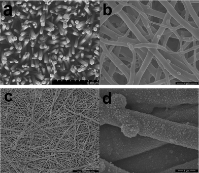 | ||
| Fig. 1 SEM photographs of (a) aligned ZnO nanorods, (b) ESM, and (c) & (d) ESM templated PANi network. | ||
Fig. 1b shows the typical SEM image of the natural ESM template used in this work. It reveals that the membrane is a macroporous network composed of interwoven and coalescing shell membrane fibers ranging in diameter from 0.5 to 1 μm. The presence of macropores with pore sizes of 1–3 μm is evident. The ESM contains amines, amides, and carboxylic surface functional groups that may interact with the aniline or pyrrole monomers, anchoring the monomer molecules to the membrane fiber surface where solution polymerization can occur. SEM images of the resultant hierarchically ordered macroporous PANi network obtained from in situpolymerization of the aniline under acidic conditions are shown in Fig. 1c & 1d. The as-obtained macroporous PANi network is composed of interwoven and coalescing PANi fibers ranging in diameter from 1 to 5 μm, slightly bigger than the diameters of the initial ESM fibers, indicating an approximate PANi thickness of 0.25–2 μm. The PANi chains are formed along the fibers without any change to the ESM conformations. Due to the presence of the ESM fibers, the resultant PANi network is flexible and can be bent many times with no breakage. Furthermore, we note that the macroporous PANi network shows little trace of granular structures. It is well-known that the strong intra- and inter-molecular H-bonding interactions in PANi molecules can lead to extensive coiling of the polymer chains, resulting in granular morphology. In such a coiled configuration, the planarity of the backbone is lost, which is expected to have an adverse effect on the π-electron delocalization. Due to the strong H-bonding and electrostatic interactions with the amines, amides, and carboxylic surface functional groups, the aniline monomer can be strongly adsorbed onto the fibers of ESM. The in situpolymerization helps to open up these coiled-up chains and achieve a chain-extended configuration, as can be seen from Fig. 1d. While in such a configuration, the electron delocalization along a single chain is much more facile, it also helps the individual chains interact better among themselves, leading to a more efficient three-dimensional delocalization of electronic wave functions. Thus, one might expect to achieve rapid hole-transport.
Structural analysis
The crystal structures of the as-grown ZnO nanorods and PANi network were identified by XRD. As shown in Fig. 2a, the positions in the XRD pattern of the aligned ZnO nanorods perfectly match the standard Powder Diffraction File values (JCPDS # 800075 file). All the diffraction peaks can be indexed to a pure wurtzite hexagonal phase of bulk ZnO.10 No impurity phase can be detected within the sensitivity limit of our XRD apparatus. The location of the strongest peak at 36.2° may originate from the oriented growth of the resultant nanorods along the c-axis in the (001) direction,11 which is consistent with the result of SEM observation. To further determine the conformational changes and also to study the crystalline structures of the macroporous PANi network, large-scale PANi network was subjected to wide-angle XRD analysis. The XRD pattern of the flexible PANi is given in Fig. 2b. The XRD pattern of the macroporous PANi network by our method shows five typical diffraction peaks at 2θ = 8.1, 13.9, 20.1, 24.7, and 27.4°. The peak centered at 2θ = 20.1° is ascribed to periodicity parallel to the polymer chain, while the peak at 2θ = 25.5° is caused by the periodicity perpendicular to the polymer chains.12–14 The three peaks at 13.9, 20.1 and 25.5° are generally observed in conventionally synthesized PANi products, but the peak at around 2θ = 8.1° is only observed for highly ordered PANi in which PANi chain distance increases by the effective interdigitation of dopant molecules.15 The peak intensity at 2θ = 8.1° indicates the ordering degree of acid doped PANi in the molecular chains. The crystallinity of the macroporous PANi network has great influence on the electrical conductivity and electrochemical property and further affects the hole-transport ability of the PANi network in the device.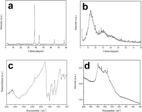 | ||
| Fig. 2 XRD pattern of the (a) aligned ZnO nanorods, and (b) XRD pattern, (c) FTIR spectrum and (d) Raman spectrum of the macroporous PANi network. | ||
Infrared spectrography is a useful technique in characterizing structures of materials. From the microtransformations in the FTIR spectra, we can detect the changes in structure and analyze the potential mechanism. Fig. 2c shows the FTIR spectrum of the macroporous PANi network. The characteristic band at 1506 cm−1 corresponds to the C![[double bond, length as m-dash]](https://www.rsc.org/images/entities/char_e001.gif) C stretching deformation mode of the benzenoid units (related to the reduced state of the polymer), while the band at 1652 cm−1 corresponds to C
C stretching deformation mode of the benzenoid units (related to the reduced state of the polymer), while the band at 1652 cm−1 corresponds to C![[double bond, length as m-dash]](https://www.rsc.org/images/entities/char_e001.gif) N stretching of the quinoid units produced when PANi is oxidized. The band at 1303 cm−1 could be interpreted as a C–N stretching vibration in the polaron structure. The aromatic C–H in-plane bending vibration mode, which is formed during protonation,16 locates at 1246 cm−1. Bands at 1145 and 694 cm−1 are the results of C–H out-of-plane bending of 1,2,4 ring and C–H out-of-plane bending of the 1,2 ring, respectively. Out-of-plane deformations of C–H on 1,4-disubstituted rings are located at 827 cm−1, and the absorption peak at 605 cm−1 is caused by the deformations of the benzene ring.17 The bands observed at 800–900 cm−1 are characteristic of para substitution of the aromatic ring and reveal that the polymerization has proceeded via a head-to-tail mechanism. Upon acid protonation of the emeraldine base, the quinonoid units are believed to be converted to benzenoid units by a proton-induced spin-unpairing mechanism. In the case of protonated emeraldine, the long absorption tail above 2000 cm−1, which masks the N–H stretching vibration in the 3100–3500 cm−1 region, and the appearance of the intense broad band at about 1246 cm−1 have been associated with high electrical conductivity and a high degree of electron delocalization in PANi.18,19 The band at 1382 cm−1 may come from the ESM template. Raman spectroscopy was also used to confirm the presence of PANi. The information in the Raman spectrum gives us an insight into the oxidation state of PANi network. The Raman spectrum of the macroporous PANi network (emeraldine) base obtained using a 633 nm excitation line contains the peak connected with the C–C and C
N stretching of the quinoid units produced when PANi is oxidized. The band at 1303 cm−1 could be interpreted as a C–N stretching vibration in the polaron structure. The aromatic C–H in-plane bending vibration mode, which is formed during protonation,16 locates at 1246 cm−1. Bands at 1145 and 694 cm−1 are the results of C–H out-of-plane bending of 1,2,4 ring and C–H out-of-plane bending of the 1,2 ring, respectively. Out-of-plane deformations of C–H on 1,4-disubstituted rings are located at 827 cm−1, and the absorption peak at 605 cm−1 is caused by the deformations of the benzene ring.17 The bands observed at 800–900 cm−1 are characteristic of para substitution of the aromatic ring and reveal that the polymerization has proceeded via a head-to-tail mechanism. Upon acid protonation of the emeraldine base, the quinonoid units are believed to be converted to benzenoid units by a proton-induced spin-unpairing mechanism. In the case of protonated emeraldine, the long absorption tail above 2000 cm−1, which masks the N–H stretching vibration in the 3100–3500 cm−1 region, and the appearance of the intense broad band at about 1246 cm−1 have been associated with high electrical conductivity and a high degree of electron delocalization in PANi.18,19 The band at 1382 cm−1 may come from the ESM template. Raman spectroscopy was also used to confirm the presence of PANi. The information in the Raman spectrum gives us an insight into the oxidation state of PANi network. The Raman spectrum of the macroporous PANi network (emeraldine) base obtained using a 633 nm excitation line contains the peak connected with the C–C and C![[double bond, length as m-dash]](https://www.rsc.org/images/entities/char_e001.gif) C vibrations in benzenoid and quinonoid rings observed at 1592 cm−1 and the band at 1492 cm−1 assigned to the C
C vibrations in benzenoid and quinonoid rings observed at 1592 cm−1 and the band at 1492 cm−1 assigned to the C![[double bond, length as m-dash]](https://www.rsc.org/images/entities/char_e001.gif) N vibration in quinonoid units, which dominates the spectrum, and a band of C–N stretching vibrations at 1335 cm−1 is observed.
N vibration in quinonoid units, which dominates the spectrum, and a band of C–N stretching vibrations at 1335 cm−1 is observed.
The UV-vis spectrum of the macroporous PANi network is conducted at room temperature and the result is presented in Fig. 3a. In the UV-vis spectrum, three peaks are detected. The peaks at around 352 nm is attributed to the polaron band → π* transition of PANi. Two bands at 432 nm and 738 nm are assigned to the π → localized polaron band. These bands indicate that H+-doped PANi is in its conducting form (i.e., the emeraldine salt).20 From the long tail located in infrared region, H+ attached to the N sites in the backbone can be expected to increase the torsional angle appended by the trans–cisazobenzene photoisomerization between adjacent rings. This will cause the extent of orbital overlap between the phenyl π electrons and the nitrogen lone pairs. This also decreases the extent of the π conjugation, resulting in increasing the energy level of πq. Fig. 3b shows the CV curves of macroporous PANi network. Experimental values of the lowest unoccupied molecular orbital (LUMO), highest occupied molecular orbital (HOMO), and band gap (Eg) of the PANi, which are important to reveal the transport mechanism, can be obtained by the CV curve and UV-vis spectrum.21,22 During the scan process, the PANi network exhibits the first oxidation peak at 0.215 V vs.Ag/AgCl. The HOMO energy level can be calculated from the first oxidation potential [Eox(onset)] based on the reference energy level of ferrocene (− 4.8 eV):
 | (1) |
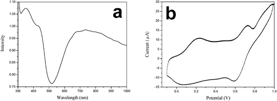 | ||
| Fig. 3 (a) UV-vis spectrum and (b) cyclic voltammogram (CV) of the macroporous PANi network. The CV was measured in 1 mM K4Fe(CN)6 + 0.15 M NaCl solution at a scan rate of 50 mV s−1. | ||
Performances of heterojunctions
Fig. 4a shows the schematic diagram describing the assembly of dye-sensitized FTO/ZnO nanorods:macroporous PANi network/Al heterojunctions. From Fig. 1, one can see that the diameter of the ZnO nanorods and pore size of the PANi network are 300 nm and 2–3 μm, respectively. Once the dye-loaded macroporous PANi network is compressed on the ZnO nanorods, the aligned nanorods can be inserted into the pores of PANi network which acts as the dye source for ZnO nanorods (Fig. 4b). ESM is a hierarchically ordered macroporous network (Fig. 5a), its backside is formed by a layer of dense microparticles (Fig. 5b). Therefore, some ZnO nanorods can penetrate the first few layers of PANi network and contact with the inner fibers. The N719 dye contains attachment groups such as carboxylate and carboxylic acid to firmly graft it to the PANi backbone and ZnO nanorods. Upon excitation it can inject electrons into the ZnO with a quantum yield of unity.23 To examine the application of the dye-sensitized FTO/ZnO nanorods:macroporous PANi network/Al heterojunction, the energy level diagram of the device is analyzed (Fig. 4c). The PANi network provides a largely rough surface area for the anchoring of sufficient N719 dye to yield high light absorption in the long wavelength region, where much of the solar flux is incident. During operation, photons intercepted by the dye molecules with a LUMO of − 3.25 eV and HOMO of − 5.05 eV create excitons that are rapidly split on the ZnO nanorod surfaces, with electrons injected into the VB (− 4.2 eV) of the ZnO nanorods and holes, leaving the opposite side to the HOMO (− 4.6 eV) of PANi because of the inherent nature of a good hole-transport material.24 Herein, the 1D ZnO nanorods produce a lower diffusion resistance than the traditional nanoparticle film facilitating the transport of charge carriers. Thus, an enhanced photocurrent could be generated in the FTO/ZnO nanorods:macroporous PANi network/Al heterojunction, which would be an effective energy source for a circuit. | ||
| Fig. 4 Schematic diagrams describing (a) the structure of dye-sensitized FTO/ZnO nanorods:macroporous PANi network/Al heterojunction, (b) interpenetration of aligned ZnO nanorods and macroporous PANi network, and (c) energy level for the device with energy levels in eV relative to vacuum. | ||
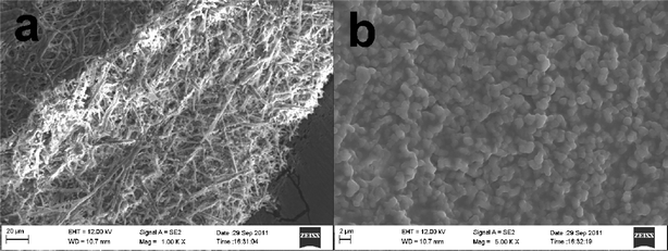 | ||
| Fig. 5 (a) Cross-sectional and (b) backside SEM views of ESM. | ||
The dark I–V characteristic of the p–n heterojunction based on the aligned ZnO nanorods:macroporous PANi network measured under various illumination intensities at room temperature show typical rectifying behaviors (Fig. 6a), indicating the formation of a diode between the ZnO nanorods and the macroporous PANi network.25,26 Li and co-workers have analyzed the formation mechanism of a p–n heterojuntion between ZnO and PANi,26 which is also applicable in the current research. The dark current is responsible for the transport of electrons involving the shallow donor (intrinsic Zn interstitial27 or/and extrinsic hydrogen28) levels to the PANi side. Both the forward and the backward currents increase with an increasing illumination intensity from zero to 100 mW cm−2. It is well known that the abundant defects on the ZnO nanorods surfaces can act as gas adsorption sites to trap oxygen molecules.29 The chemisorbed oxygen can capture free electrons in the darkness from the conduction band of ZnO nanorods and form oxygen ions (O2−), creating a depletion layer at the interface of ZnO and PANi and resulting in a low current. Under visible light illumination, partial photogenerated holes migrate to the surface of ZnO nanorods and are neutralized by the negatively charged surface O2− ions,30 leaving the excited electrons unpaired. Therefore, there is an increased current flow through the junction and the external circuit for both the forward and reverse biases under visible light illumination. Interestingly, the rectification ratio (defined as the forward current divided by the backward current at a bias) as shown in Fig. 6b shows a linear relationship between the rectification ratio (R) and illumination intensity (P), which can be fitted by equation of R = 7.43 × 10⁻⁴P + 1.05.
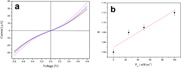 | ||
| Fig. 6 (a) Current–voltage (I–V) curve of FTO/ZnO nanorods:macroporous PANi network/Al heterojunction under various illumination intensities: 0 (black), 25 (red), 50 (blue) and 100 mW cm−2 (magenta). (b) The rectification ratio as a function of illumination intensity. | ||
The I–V characteristics of the dye-sensitized FTO/ZnO nanorods:macroporous PANi network/Al heterojunction were measured under illumination intensities ranging from 0 to 100 mW cm−2 (Fig. 7a). Compared with the bared FTO/ZnO nanorod![[thin space (1/6-em)]](https://www.rsc.org/images/entities/char_2009.gif) :
:![[thin space (1/6-em)]](https://www.rsc.org/images/entities/char_2009.gif) macroporous PANi network/Al heterojunction, a strong increase in the forward and the backward currents and rectification ratio was observed in the dye-sensitized heterojunction under the same illumination intensity. To explore the potential mechanism, much more photons were intercepted by the dye molecules which created excitons that were rapidly split at the ZnO nanorod surfaces, producing more electrons and holes. Also, a linear relationship between R and the illumination intensity was observed in Fig. 7b, showing R = 5.78 × 10⁻³P + 2.62. Overall, the FTO/ZnO nanorods:macroporous PANi network/Al heterojunction acts as a diode and exhibits typical rectifying properties under visible illumination at room temperature. These characters are highly desirable for high performance light photodetectors and the optoelectronic devices.
macroporous PANi network/Al heterojunction, a strong increase in the forward and the backward currents and rectification ratio was observed in the dye-sensitized heterojunction under the same illumination intensity. To explore the potential mechanism, much more photons were intercepted by the dye molecules which created excitons that were rapidly split at the ZnO nanorod surfaces, producing more electrons and holes. Also, a linear relationship between R and the illumination intensity was observed in Fig. 7b, showing R = 5.78 × 10⁻³P + 2.62. Overall, the FTO/ZnO nanorods:macroporous PANi network/Al heterojunction acts as a diode and exhibits typical rectifying properties under visible illumination at room temperature. These characters are highly desirable for high performance light photodetectors and the optoelectronic devices.
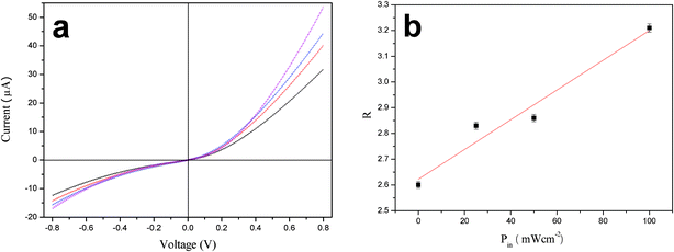 | ||
| Fig. 7 (a) Current–voltage (I–V) curve of dye-sensitized FTO/ZnO nanorods:macroporous PANi network/Al heterojunction under various illumination intensities: 0 (black), 25 (red), 50 (blue) and 100 mW cm−2 (magenta). (b) The rectification ratio as a function of illumination intensity. | ||
4. Conclusions
In conclusion, the results of our study have demonstrated N719 dye-sensitized FTO/ZnO nanorods:macroporous PANi network/Al heterojunctions. The SEM observations revealed that the average diameter of the aligned ZnO nanorods is 300 nm and the diameter of macroporous PANi network composing of interwoven and coalescing PANi fibers is in the range of 1 ∼ 5 μm with a pore size of 1 ∼ 3 μm. The good electron transport in crystalline ZnO nanorods and hole transport in the PANi network exhibit a rectification ratio of 3.21 under an illumination intensity of 100 mW cm−2, which is higher than 1.12 in the bared heterojunction. The insertion of ZnO nanorods into the macroporous PANi network and the dye loading in the network to provide a dye source which is used for photon trapping. The fundamental studies in the current work will be definitely helpful to understand the work mechanism of aligned inorganic semiconductor/porous conjugated polymer heterojunctions, and to set a bridge between well-aligned, continuous and crystalline inorganic nanostructures and network-fabricated conjugated polymers and modern photovoltaic devices.Acknowledgements
The authors gratefully acknowledge the financial support of the National High Technology Research and Development Program of China (No. 2009AA03Z217), the National Natural Science Foundation of China (No. 90922028).References
- R. Charvet, S. Acharya, J. P. Hill, M. Akada, M. Liao, S. Seki, Y. Honsho, A. Saeki and K. Ariga, J. Am. Chem. Soc., 2009, 131, 18030–18031 CrossRef CAS.
- T. Lohmann, K. Klitzing and J. H. Smet, Nano Lett., 2009, 9, 1973–1979 CrossRef CAS.
- D. C. Olson, S. E. Shaheen, R. T. Collins and D. S. Ginley, J. Phys. Chem. C, 2007, 111, 16670–16678 CAS.
- A. Joshi, D. K. Aswal, S. K. Gupta, J. V. Yakhmi and S. A. Gangal, Appl. Phys. Lett., 2009, 94, 103115–103117 CrossRef.
- M. Nakano, T. Makino, A. Tsukazaki, K. Ueno, A. Ohtomo, T. Fukumura, H. Yuji, S. Akasaka, K. Tamura, K. Nakahara, T. Tanabe, A. Kamisawa and M. Kawasaki, Appl. Phys. Lett., 2008, 93, 123309 CrossRef.
- M. Chang, X. Cao and H. Zeng, J. Phys. Chem. C, 2009, 113, 15544–15547 CAS.
- E. B. Salomsom, M. B. Munoz, R. M. Vequizo and E. P. Jacosalem, http://physics.msuiit.edu.ph/spvm/papers/2005/salomsom.pdf..
- B. C. Das, S. K. Batabyal and A. J. Pal, Adv. Mater., 2007, 19, 4172–4176 CrossRef CAS.
- R. B. Peterson, C. L. Field and B. A. Gregg, Langmuir, 2004, 20, 5114–5118 CrossRef CAS.
- Q. W. Tang, J. H. Wu, Y. Li, J. M. Lin, Z. Y. Tang and M. L. Huang, J. Mater. Chem., 2011, 21, 12927–12934 RSC.
- P. Jiang, J. J. Zhou, H. F. Fang, C. Y. Wang, Z. L. Wang and S. S. Xie, Adv. Funct. Mater., 2007, 17, 1303–1310 CrossRef CAS.
- Q. W. Tang, X. M. Sun, Q. H. Li, J. H. Wu and J. M. Lin, Langmuir, 2009, 25, 5253–5257 CrossRef CAS.
- J. H. Wu, Q. W. Tang, Q. H. Li and J. M. Lin, Polymer, 2008, 49, 5262–5267 CrossRef CAS.
- P. Anilkumar and M. Jayakannan, Macromolecules, 2007, 40, 7311–7319 CrossRef CAS.
- W. Lunzy and E. Banka, Macromolecules, 2000, 33, 425–429 CrossRef.
- A. Zimmermann, U. Kunzelmann and L. Dunsch, Synth. Met., 1998, 93, 17–25 CrossRef CAS.
- M. Trchova, I. Sedenkova, E. Tobolkova and J. Stejskal, Polym. Degrad. Stab., 2004, 86, 179–185 CrossRef CAS.
- J. Tang, X. Jing, B. Wang and F. Wang, Synth. Met., 1988, 24, 231–238 CrossRef CAS.
- F. L. Lu, F. Wudl, M. Nowak and A. J. Heeger, J. Am. Chem. Soc., 1986, 108, 8311–8313 CrossRef CAS.
- J. Kim, S. Cho, S. Choi, S. Baek, D. Lee, O. Kim, S. M. Park and M. Ree, Langmuir, 2007, 23, 9024–9030 CrossRef CAS.
- S. L. Lim, N. J. Li, J. M. Lu, Q. D. Ling, C. X. Zhu, E. T. Kang and K. G. Neoh, ACS Appl. Mater. Interfaces, 2009, 1, 60–71 CAS.
- Y. Z. Lee, X. W. Chen, S. A. Chen, P. K. Wei and W. S. Fann, J. Am. Chem. Soc., 2001, 123, 2296–2307 CrossRef CAS.
- M. Grätzel, J. Photochem. Photobiol., A, 2004, 164, 3–14 CrossRef.
- Q. H. Li, J. H. Wu, Q. W. Tang, Z. Lan, P. J. Li, J. M. Lin and L. Q. Fan, Electrochem. Commun., 2008, 10, 1299–1302 CrossRef CAS.
- S. Mridha and D. Basak, Appl. Phys. Lett., 2008, 92, 142111–142113 CrossRef.
- Y. H. Li, J. Gong, M. McCune, G. H. He and Y. L. Deng, Synth. Met., 2010, 160, 499–503 CrossRef CAS.
- A. F. Kohan, G. Ceder, D. Morgan and C. G. Van de Walle, Phys. Rev. B: Condens. Matter, 2000, 61, 15019–15027 CrossRef CAS.
- C. G. Van de Walle, Phys. Rev. Lett., 2000, 85, 1012–1015 CrossRef CAS.
- . C. S. Lao, M. C. Park, Q. Kuang, Y. L. Deng, A. K. Sood, D. L. Polla and Z. L. Wang, J. Am. Chem. Soc., 2007, 129, 12096–12097 CrossRef.
- C. Soci, A. Zhang, B. Xiang, S. A. Dayeh, D. P. R. Aplin, J. Park, X. Y. Bao, Y. H. Lo and D. Wang, Nano Lett., 2007, 7, 1003–1009 CrossRef CAS.
| This journal is © The Royal Society of Chemistry 2012 |
