Fast one-step silicon–hydrogen bond assembly of silver nanoparticles as excellent surface-enhanced Raman scattering substrates†
Qi
Shao
ab,
Ronghui
Que
a,
Liang
Cheng
a and
Mingwang
Shao
*a
aInstitute of Functional Nano and Soft Materials (FUNSOM) & Jiangsu Key Laboratory for Carbon-based Functional Materials and Devices, Soochow University, Suzhou, Jiangsu 215123, P. R. China. E-mail: mwshao@suda.edu.cn; Fax: +86-512-65882846; Tel: +86-512-65880953
bDepartment of Chemistry, Hefei National Laboratory for Physical Sciences at the Microscale, The University of Science and Technology of China, Hefei, Anhui 230026, P. R. China
First published on 13th January 2012
Abstract
A one-step method was reported to directly fabricate efficient surface-enhanced Raman scattering substrates based on the silicon–hydrogen bond assembly of Ag nanoparticles on a Si wafer, exhibiting an excellent surface-enhanced Raman effect in the low concentration detection (1 × 10⁻¹² M) of Rhodamine 6G and Sudan I with relative standard deviation (RSD) of <20%.
Since the first discovery of surface-enhanced Raman scattering (SERS) in the 1970s,1 several techniques have been developed for directing the self-assembly of nanocrystals into ordered aggregates, such as electron beam lithography,2,3 Langmuir–Blodgett assembly,4,5nanosphere lithography,6,7 noncovalent interactions,8 bifunctional organic molecules,9thiol groups,10surfactants,11proteins,12DNA,13polymers,14,15 bi-solvent interfaces,16 and capillary-assisted routes,17,18 which have been used to guarantee the highly reproducibility and stability of substrates.
Nevertheless, the formation of nanoparticles (NPs) based on architectures with well-defined geometric morphology remains a challenge to circumvent.19 Specifically, the above assembly methods exhibit shortcomings that cannot be qualified for prominent SERS substrates: (1) the process is often time-consuming, and two or more steps were required;20 (2) the common additives in the synthetic procedure, such as surfactants, would unnecessarily influence the SERS effect;20 (3) the effective area of SERS substrates is extremely limited because of the synthetic methods;17 (4) lastly, but most importantly, the outstanding localized surface plasmon resonance induced from assembly readily causes the aggregation and growth of metal under laser irradiation in the SERS detection.21
Here we report a one-step assembly of highly ordered Ag NPs on Si wafer scale without any templates or surfactants. The Ag NPs were epitaxially grown on the Si wafer via the reduction of silicon–hydrogen bonds,22 which made it difficult for them to grow larger under the laser irradiation. The average size of the Ag NPs is easily controllable under 30 nm. In addition, the assembly was time-saving, taking only a few seconds. More significantly, the highly ordered Ag NPs on the Si wafer acted as a probe for SERS testing, and demonstrated highly sensitive enhancement for Rhodamine 6G (R6G) and Sudan I (SDI). All of these above mentioned excellent properties would bring great convenience for practical detection.
The Si wafers were cut to a size of 1 cm × 1 cm and cleared sequentially with acetone, ethanol, H2SO4/H2O2, and water. Then, Ag2SO4 (0.0312 g, 1 × 10⁻⁴ mol), 10 mL distilled water and 5 mL 4% HF solutions were mixed and stirred in a Teflon beaker at room temperature. Then the cleared Si wafers were placed in the above solution for just 2 s, taken out, rinsed with distilled water, and dried at room temperature. In this process, the oxide layers of the Si wafers were removed by HF and Si–H bonds covered the surface. These Si–H bonds chemically reduced silver ions to elemental Ag. Therefore, the Ag NPs were in situ assembled on the Si wafers.
In order to weaken the influence of surface-enhanced resonance Raman scattering, a 633 nm He-Ne laser was employed in all the Raman detections.
Fig. 1 shows a schematic of Si–H bond assembly of Ag NPs on a Si wafer, which was based on the following consideration: there always exists an oxide layer on the surface of a Si wafer. When this oxide was removed using HF solution, the wafer was intensively covered with hydrogen atoms (Si–H), which have the ability to reduce Ag ions.22 Therefore, Ag NPs may grow in situ and assemble on the Si wafer densely. Because the Si–H bond plays a pivotal role in the experiment, we name this process “silicon–hydrogen bond assembly”.
 | ||
| Fig. 1 Schematic of Si–H bond assembly of Ag NPs on a Si wafer. | ||
An XRD pattern of Ag NPs assembling on a Si wafer is shown in Fig. S1 (ESI†), confirming the formation of silver. And an SEM image of the assembly is shown in Fig. S2 (ESI†), which exhibits the highly uniform Ag NPs. Also, according to the AFM image (Fig. 2a), the average diameter of the as-prepared Ag NPs was determined to be 30 nm.
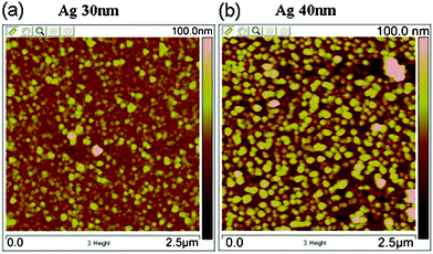 | ||
| Fig. 2 AFM images of Ag NPs (a) before and (b) after SERS detection. | ||
In order to evaluate the SERS of the Ag NP assembly, Raman spectra were collected employing R6G as the probe molecule owing to its well-established vibrational features.
A Si wafer assembled with Ag NPs was first immersed in 1 × 10⁻¹² M R6G methanol solution for 1 h, and rinsed with alcohol. After drying, SERS detection was carried out. The substrate exhibited remarkable SERS activity (upper part of Fig. 3). The obvious peaks of R6G's main vibrations in SERS, the strongest bands of carbon skeleton stretching modes at 1366, 1512, 1576, and 1650 cm−1,23 were similar to those of the normal powder Raman spectrum24 as shown in Fig. S3 (ESI†). There were also some bands centered at 1130 and 1599 cm−1 distinctly observed in the SERS, which were hardly observable in the normal Raman spectrum. The appearance of these bands proved the enhancement effect of the substrate.
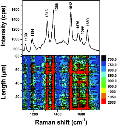 | ||
| Fig. 3 The SERS spectrum of R6G methanol solution (1 × 10⁻¹² M) on Ag NP assembly as substrate (upper part), and the SERS contour (lower part). | ||
This high SERS activity was possibly a benefit of the large electromagnetic field coupling at the junctions of the NPs.25,26 The density of Ag NPs is larger than 230 particles per square micrometre based on the AFM image (Fig. 2). Therefore, the interparticle distance among the adjacent Ag NPs was much less than the laser spot size in the Raman detection, which was calculated to be 0.86 μm according to the formula27D = 1.22 λ/NA, where λ is the wavelength of the laser used and NA is the numerical aperture of the objective. Thus the laser spot covers over one hundred Ag NPs (π × (0.86/2)2 × 230 = 133), which ensures the sensitivity and reproducibility of SERS.
Another critical point shown in the lower part of Fig. 3 is the exceptional uniformity of the substrate. The SERS contour was plotted after the line mapping which was conducted spot-to-spot at 1 × 10⁻¹² M R6G methanol solution. In all the 82 spots, each spot exhibited a favorable capability to enhance Raman signals of the R6G molecules.
To further semi-quantitatively assess the uniformity of these SERS signals, the relative standard deviation (RSD) of the intensity of the carbon skeleton stretching modes was calculated. The values of RSD of vibrations at 1313, 1366, 1512, and 1650 cm−1 (Fig. 4) are 16.3%, 19.8%, 18.3%, and 15.5%, respectively, which could vigorously indicate the uniformity of the substrate.28 Less than 20% of the RSD of the four bands in Fig. 4 further demonstrated that the as-prepared assembly was suitable for a highly sensitive SERS substrate.29
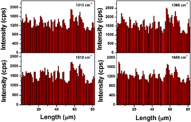 | ||
| Fig. 4 The intensities of the main Raman vibrations of R6G methanol solution (1 × 10⁻¹² M) in 82 spot SERS line-scan spectra collected on the Ag NP assembly. | ||
The Ag NP assembly was also used to detect 1× 10⁻¹² M SDI methanol solution, a common dye in plastics, oil paint, printing, and dyeing, but banned for use in food production due to its damage to DNA, RNA and enzymes.30
The SERS spectrum from the SDI-coated assembly (Fig. 5, upper part) is similar to the normal powder Raman spectrum of SDI powder (Fig. S4†). The SERS contour (Fig. 5, lower part) was obtained from the line mapping conducted spot-to-spot on the Ag NP assembly coated with 1 × 10⁻¹² M SDI methanol solution. For all the 82 spots, each spot exhibits the strong SERS signals. The values of the RSD of the Raman vibrations at 1230 and 1598 cm−1 are 17.3% and 18.4%, respectively (Fig. 6), further confirming the remarkable enhancement effect and high uniformity of the assembly.
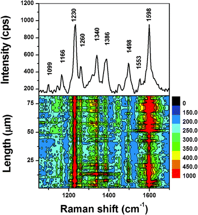 | ||
| Fig. 5 The SERS spectrum of SDI methanol solution (1 × 10⁻¹² M) on Ag NP assembly as substrate (upper part), and the SERS contour (lower part). | ||
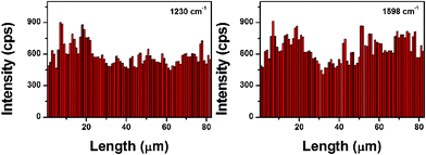 | ||
| Fig. 6 The intensities of the main Raman vibrations of SDI methanol solution (1 × 10⁻¹² M) in 82 spot SERS line-scan spectra collected on the Ag NP assembly. | ||
It should be pointed out that apart from the mentioned electromagnetic field coupling, the crystal lattice matching is another critical factor for the SERS effect. Si and Ag belong to a face-centered cubic phase with crystal parameters of 0.5430 and 0.4086 nm, respectively. There exists a simple proportional relationship between these values, that is, aSi![[thin space (1/6-em)]](https://www.rsc.org/images/entities/char_2009.gif) :
:![[thin space (1/6-em)]](https://www.rsc.org/images/entities/char_2009.gif) aAg = 4
aAg = 4![[thin space (1/6-em)]](https://www.rsc.org/images/entities/char_2009.gif) :
:![[thin space (1/6-em)]](https://www.rsc.org/images/entities/char_2009.gif) 3, with a lattice mismatch rate of less than 0.34% ((4 × 0.4086 − 5 × 0.5430)/(4 × 0.4086) = 0.34%). The above values indicate that Ag NPs may epitaxially grow on a Si wafer. And the epitaxial growth resulted in a strong adhesion between the Si wafer and the Ag NPs, and made it difficult for these NPs to aggregate or grow larger in the SERS detection, because Ag NPs usually grow large in the SERS detection due to the thermal effects of the laser and the surface plasmon. This phenomenon is harmful to the stability of SERS. In this work, the diameter of the Ag NPs only increased to 40 nm (Fig. 2b) after the SERS detection of R6G, which indicated that the epitaxial growth was an effective way to keep the Ag NPs from growing larger.
3, with a lattice mismatch rate of less than 0.34% ((4 × 0.4086 − 5 × 0.5430)/(4 × 0.4086) = 0.34%). The above values indicate that Ag NPs may epitaxially grow on a Si wafer. And the epitaxial growth resulted in a strong adhesion between the Si wafer and the Ag NPs, and made it difficult for these NPs to aggregate or grow larger in the SERS detection, because Ag NPs usually grow large in the SERS detection due to the thermal effects of the laser and the surface plasmon. This phenomenon is harmful to the stability of SERS. In this work, the diameter of the Ag NPs only increased to 40 nm (Fig. 2b) after the SERS detection of R6G, which indicated that the epitaxial growth was an effective way to keep the Ag NPs from growing larger.
Si–H bond assembly is a highly-effective and time-saving approach to fabricate uniform Ag NP assemblies on Si wafers. This method presents a new strategy for designing practical SERS substrates, which offer numerous significant merits over conventional SERS substrates. These assemblies exhibited outstanding SERS activity with high uniformity and reproducibility. They also offered various significant benefits including low-cost, mechanical robustness, and easy control.
Financial support from the National Nature Science Fund of China (No. 21071106) and the 973 Project of China (No. 2012CB932900) are appreciated.
References
- M. Fleischmann, P. J. Hendra and A. J. McQuillan, Chem. Phys. Lett., 1974, 26, 163 CrossRef CAS.
- L. Polavarapu and Q. H. Xu, Langmuir, 2008, 24, 10608 CrossRef CAS.
- Q. M. Yu, P. Guan, D. Qin, G. Golden and P. M. Wallace, Nano Lett., 2008, 8, 1923 CrossRef CAS.
- A. Tao, F. Kim, C. Hess, J. Goldberger, R. R. He, Y. G. Sun, Y. N. Xia and P. D. Yang, Nano Lett., 2003, 3, 1229 CrossRef CAS.
- Y. Lu, G. L. Liu and L. P. Lee, Nano Lett., 2005, 5, 5 CrossRef CAS.
- D. Fava, Z. H. Nie, M. A. Winnik and E. Kumacheva, Adv. Mater., 2008, 20, 4318 CrossRef CAS.
- J. C. Hulteen and R. P. Van Duyne, J. Vac. Sci. Technol., A, 1995, 13, 1553 Search PubMed.
- J. Rebek, Acc. Chem. Res., 1999, 32, 278 CrossRef CAS.
- L. Guerrini, I. Izquierdo-Lorenzo, J. V. Garcia-Ramos, C. Domingo and S. Sanchez-Cortes, Phys. Chem. Chem. Phys., 2009, 11, 7363 RSC.
- D. Y. Wu, X. M. Liu, Y. F. Huang, B. Ren, X. Xu and Z. Q. Tian, J. Phys. Chem. C, 2009, 113, 18212 CAS.
- H. Wang, C. S. Levin and N. J. Halas, J. Am. Chem. Soc., 2005, 127, 14992 CrossRef CAS.
- X. X. Han, L. Chen, J. Guo, B. Zhao and Y. Ozaki, Anal. Chem., 2010, 82, 4102 CrossRef CAS.
- G. Wei, L. Wang, Z. G. Liu, Y. H. Song, L. L. Sun, T. Yang and Z. Li, J. Phys. Chem. B, 2005, 109, 23941 CrossRef CAS.
- J. C. Heckel, L. M. Kisley, J. M. Mannion and G. Chumanov, Langmuir, 2009, 25, 9671 CrossRef CAS.
- T. Chen, H. Wang, G. Chen, Y. Wang, Y. H. Feng, W. S. Teo, T. Wu and H. Y. Chen, ACS Nano, 2010, 4, 3087 CrossRef CAS.
- K. Kim, H. B. Lee, J. W. Lee, H. K. Park and K. S. Shin, Langmuir, 2008, 24, 7178 CrossRef CAS.
- R. H. Que, M. W. Shao, S. J. Zhuo, C. Y. Wen, S. D. Wang and S. T. Lee, Adv. Funct. Mater., 2011, 21, 3337 CrossRef CAS.
- F. S. Ou, M. Hu, I. Naumov, A. Kim, W. Wu, A. M. Bratkovsky, X. M. Li, R. S. Williams and Z. Y. Li, Nano Lett., 2011, 11, 2538 CrossRef CAS.
- P. K. Sudeep, S. T. S. Joseph and K. G. Thomas, J. Am. Chem. Soc., 2005, 127, 6516 CrossRef CAS.
- X. M. Feng, F. X. Ruan, R. J. Hong, J. S. Ye, J. Q. Hu, G. Q. Hu and Z. L. Yang, Langmuir, 2011, 27, 2204 CrossRef CAS.
- K. H. Yang, Y. C. Liu, T. C. Hsu and M. Y. Juang, J. Mater. Chem., 2010, 20, 7530 RSC.
- M. W. Shao, L. Cheng, D. D. D. Ma and S. T. Lee, J. Am. Chem. Soc., 2009, 131, 17738 CrossRef CAS.
- P. Hildebrandt and M. Stockburger, J. Phys. Chem., 1984, 88, 5935 CrossRef CAS.
- M.W. Shao, L. Lu, H. Wang, S. Wang, M. L. Zhang, D. D. D. Ma and S. T. Lee, Chem. Commun., 2008, 2310 RSC.
- S. M. Nie and S. R. Emory, Science, 1997, 275, 1102 CrossRef CAS.
- K. Kneipp, Y. Wang, H. Kneipp, L. T. Perelman, I. Itzkan, R. R. Dasari and M. S. Feld, Phys. Rev. Lett., 1997, 78, 1667 CrossRef CAS.
- S. Nakashima and M. Hangyo, IEEE J. Quantum Electron., 1989, 25, 965–975 CrossRef CAS.
- H. Y. Liang, Z. P. Li, W. Z. Wang, Y. S. Wu and H. X. Xu, Adv. Mater., 2009, 21, 4614 CrossRef CAS.
- M. J. Natan, Faraday Discuss., 2006, 132, 321 RSC.
- M. L.Zhang, X. Fan, H. W. Zhou, M. W. Shao, J. A. Zapien, N. B. Wong and S. T. Lee, J. Phys. Chem. C, 2010, 114, 1969 Search PubMed.
Footnote |
| † Electronic supplementary information (ESI) available: Chemicals and characterization details, XRD pattern, SEM image and Raman spectra. See http://dx.doi.org/10.1039/c2ra00971d/ |
| This journal is © The Royal Society of Chemistry 2012 |
