DOI:
10.1039/C2RA01030E
(Paper)
RSC Adv., 2012,
2, 3791-3800
Core-shell Au–TiO2 nanoarchitectures formed by pulsed laser deposition for enhanced efficiency in dye sensitized solar cells†
Received
3rd November 2011
, Accepted 12th February 2012
First published on 8th March 2012
Abstract
Vertically aligned Au–TiO2 core–shell nanowires were synthesized by using a two step method. Au nanowires were first synthesized using a galvanostatic constant current electrodeposition technique. A shell of anatase TiO2 was subsequently grown on the Au nanowires using pulsed laser deposition. The core–shell nanostructures were then characterized using electron microscopy, electron diffraction, and X-ray diffraction techniques. The results showed that the wires were highly aligned and well separated. Dye sensitized solar cells were then fabricated using the core–shell nanowire arrays as photoanode, N535 dye as the sensitizer and I3−/I− as the redox electrolyte. The Au nanowires inside the highly crystalline TiO2 anatase nanoshell provided a direct conduction path and improved transport for electrons between the TiO2 and the conducting substrate. This efficient electron conduction out of the oxide semiconductor enhanced the current generation as well as the power conversion efficiency of the cell. The influence of the TiCl4 post-treatment on Au–TiO2 core–shell nanowire electrodes is investigated and compared to nontreated films. Cell efficiencies are improved, due to higher photocurrents as a result of this post-treatment. Optical effects of the metal nanowire may have also contributed to improved performance.
Introduction
Limited energy resources present an important problem for society in the 21st century. Solar energy, as a clean and renewable energy source, is expected to replace fossil fuels. Dye sensitized solar cells (DSSCs) have been studied as attractive alternatives for electricity generation from solar light due to their high efficiency and cost effectiveness.1 In a DSSC, a dye adsorbed onto the mesoporous TiO2 electrode absorbs a photon from solar light and forms an excited state dye which can be thought of as an electron-hole pair exciton. The excited dye transfers an electron to the semiconducting TiO2 and the electron is then transferred to the conducting substrate electrode. This process separates the electron-hole pair, leaving the hole on the dye. The hole is filled by an electron from the iodide ion supplied by the (I3−/I−) redox couple. Even though nanoparticle films provide high surface area for dye adsorption, the electron transport rate in the TiO2 is comparatively slow because of low electron diffusion coefficients. The slow diffusion is caused by TiO2 nanoparticles having multiple trapping and de-trapping events occurring in the porous semiconductor grain boundaries.2 Previous results clearly show that the electron transport process in disoriented polycrystalline mesoscopic thin films is vulnerable to trap limited electron diffusion and recombination losses at the particle interface since the electrons travel by a random walk through the network of interconnected oxide nanoparticles.3,4 This effect is likely a main cause of the high interface recombination reaction rates and limits the device efficiency. Thus, to resolve these problems, many attempts have been put forth to improve the state-of the-art DSSC design. A DSSC based on an array of one-dimensional (1D) ZnO nanostructures was first introduced by Law et al. in 2005,5 and there are reports of synthesizing nanoparticles/nanowire composites6 and nanoparticles/nanotube composites7 of TiO2 anatase phase with an aim of achieving enhanced efficiency with a good conducting media. Particularly, DSSCs made of TiO2 ordered structures as photoanode can produce improved solar cell devices due to the prolonged stability of the anatase phase, faster electron transport, and slower charge recombination. However, despite all these positive aspects of TiO2 nanoarchitectures as photoanodes in DSSCs, the wide band gap (3.2 eV) permits only use of ultraviolet light without a dye sensitizer. The need of decreasing the recombination of electrons and holes generated by band gap excitation persists, and TiO2 solar cell efficiency is limited due to the bulk defects and grain boundaries which are important causes of limited photoconversion efficiency. Three dimensional core–shell structures having TiO2 as shell and various guest metal/metal oxide as core via electrodeposition have been reported.8–13 Zhu et al. reported metal nanoparticle chains and rods inside TiO2 nanotubes using an alumina membrane as template.14,15 There are also reports of metal doped TiO2 nanobelts,16 metal coated TiO2 nanotubes17 and metal oxide TiO2 nanorod-nanotube arrays18 with suggested application as photoanode materials in photovoltaics. There are a few reports on using nanoparticle decorated ZnO–TiO2 core–shell nanorod arrays19 and of two different wide band gap semiconductors as anodes in DSSCs.20–23 Additional work applied carbon nanofiber (CNF)-TiO2 core–shell photoanode materials in DSSCs24–28 which provided easy, uninterrupted transport of electrons from the semiconductor to the collecting anode. The efficiency remained in the 1–5% range. Various explanations have been proposed for why the above approaches failed to enhance the performance of DSSCs, including lower surface area at the semiconductor surface for dye loading29 and high series resistance between the nanostructure and the electrodes.30 A thorough knowledge and critical explanation of the above new architectures is still required in order to address the mechanisms and behavior.
One possible way to boost DSSC power conversion efficiency is to increase the diffusion length, Ln, of electrons within the oxide layer relative to the thickness of the oxide film, d, so that, Ln/d ≫ 1 and d > α−1, where α is the wavelength dependent absorption coefficient of the dye film.20 Current can be increased by making Ln ≫ d. The best TiO2 cells have Ln/d ≤ 2.31 A higher Ln/d ratio of the nanocrystalline film can be achieved by decreasing d while maintaining d > α−1 by using high molar absorption coefficient dyes32 or TiO2 semiconductors with very high surface areas.33
Since one of the major problems in achieving high efficiency is poor electron transport, we have synthesized Au–TiO2 core–shell nanowires to overcome this barrier. The motivation of this study was to create a semiconductor morphology that can provide both high surface area for maximum dye adsorption and efficient electron transport that delivers the electrons to the back contact with minimal recombination. The core–shell nanowires provided an easy pathway for electron conduction from the TiO2 layer through the Au core while maintaining the thickness of the TiO2 layer much smaller than the mean electron diffusion length which is reportedly in the range of 10–20 μm for mesoporous films.34 Au nanowires were fully coated with a 30–50 nm layer of anatase with a large TiO2 surface area available for dye adsorption. There are very few reports on the fabrication of core–shell structures and their use as electrodes in DSSC. Chou et al. first reported a nanostructure for DSSC based on indium tin oxide (ITO) coated with a TiO2 layer.35 Joanni et al. reported the synthesis of ITO-TiO2 core–shell nanowires and their application as photoanodes in DSSCs36 followed by Ye et al. who have achieved template based synthesis of nanowire-nanotube hybrid arrays37 and Wang et al. who used electrophoretic deposition to achieve ITO-TiO2 nanowires.38 We have previously prepared core–shell Au–TiO2 nanostructures for photovoltaics using a sol–gel approach.39 In this approach, we adopted a template based method for preparing these nanostructures because there are a number of useful features associated with this method. For example, it allows flexibility in tuning the length and diameter of the nanowires. We have used porous alumina membranes (also known as anodic aluminum oxide, AAO) to synthesize our photoanode materials.
Experimental methods
Preparation of Au–TiO2 core–shell nanowires
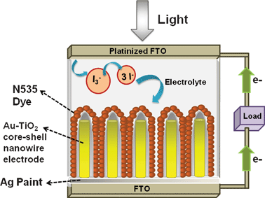
Au nanowires were synthesized by a previously reported method.40 We have used porous alumina membranes as templates to grow Au nanowires using galvanostatic constant current electrodeposition. AAO membranes (Whatman Corp.) were 25 mm in diameter, had an average pore diameter of 200 nm, and had a thickness of 60 μm. Electrochemical deposition was accomplished by converting the AAO into a working electrode (cathode) by sputtering one side with Ag (∼20 nm thick). The Ag film side was attached to one side of a piece of two sided copper tape (3 M) with the polymer coating intact on the opposite side to avoid undesired metal deposition on the Ag film or copper during electroplating. The AAO was fixed with an alligator clip and was immersed in the plating solution with the open pores exposed to the electroplating solution. The other side of the alligator clip was connected to the potentiostat. A platinum wire was used as the counter electrode and Ag/AgCl (Accumet) was used as the reference electrode. The Au plating solution (Orotemp 24) was purchased from Technic, Inc. Electrodeposition was carried out at room temperature using galvanostatic constant current of −0.9 mA with a single channel potentiostat/galvanostat (Model 263A, EG&G Instruments) to grow Au nanowires in the nanopores of the AAO membrane. It took 60 min to grow 3–4 μm long Au nanowires. The sample was washed with deionized (DI) water several times. The AAO membrane was dissolved using 3 M NaOH and washed with DI water to remove the NaOH residue. Finally, the sample was dried in air to achieve the arrays of Au nanowires standing vertically on the Cu tape. The Au–TiO2 core–shell nanowire arrays were fabricated by pulsed laser deposition (PLD) of a TiO2 shell on the gold nanowire array. PLD is a very unique technique that uses laser pulses to ablate the specified target to produce the depositing flux. The flux is subsequently deposited on the substrate facing the target to create the desired crystals. The depositing species arrive in short bursts in the order of 10–100 μs. The kinetic energy of the depositing ions is of the order of 10–100 eV. There is a report in which the authors have used this PLD to synthesize transparent semiconducting CuI thin films and applied them as photoanode material in DSSCs.41 Others have synthesized nanocrystalline TiO2 thin films on conducting ITO substrates using PLD and later used them as anodes in DSSCs.42–44 In our case, the Au nanowire arrays were employed as the substrate and the target was a TiO2 anatase pellet. A 12 mm diameter TiO2 pellet was prepared by pressing anatase TiO2 nanopowder of 30–40 nm in diameter (Aldrich) with a Carver manual pellet press and then sintering at 500 °C for 12 h. A neodymium-doped yttrium aluminum garnet (Nd:YAG) laser was used to ablate the TiO2 disc target. The laser wavelength, energy density, deposition time and repetition were 266 nm, 650 mJ cm−2, ∼30 min and 5 Hz, respectively. The distance from the target to the substrate was 3 cm. During the deposition, the pressure in the system was pumped to ∼10−3 torr and the temperature was kept at 500 °C in order to preserve the anatase phase and stoichiometry of TiO2. The Au–TiO2 nanostructures came off of the Cu tape due to the melting of the glue at the elevated temperature during the PLD process. However, the nanostructures were supported by the ∼20 nm Ag film that was sputtered onto the AAO membrane prior to electrodeposition. The core–shell nanostructures were pasted onto a fluorine doped tin oxide (FTO) glass substrate obtained from Solaronix (TCO10-10, sheet resistance 10 Ω sq−1) by means of conducting Ag paint (Ted Pella) in order to make the back side (Pt) illuminated DSSCs. To make front side (core–shell nanowire) illuminated DSSCs, the Ag film was etched away first by conc. HNO3 and the resulting Au–TiO2 core–shell nanowire array was pasted onto a FTO substrate (see Fig. S1 and S2 in the ESI† for details concerning transfer of nanostructures onto FTO for both back side and front side illuminated DSSCs). The resulting Au–TiO2 nano structures on the FTO were sensitized for 24 h by soaking in dye solution. A ruthenium dye solution (N-535, Solaronix) was prepared by mixing 25 mg of the solid in 1 mL of ethanol.
Preparation of platinized counter electrode and electrolyte
A platinum coated FTO counter electrode was prepared by brushing with a thin layer of Platisol T (Solaronix). The I−/I3− electrolyte was prepared using 0.6 M 1-methyl-3-propylimidazolium iodide, 0.05 M iodine, 0.05 M LiI and 0.5 M tert-butylpyridine in 25 mL acetonitrile/valeronitrile (1![[thin space (1/6-em)]](https://www.rsc.org/images/entities/char_2009.gif) :1 volume ratio). Two small holes were drilled in the glass of the platinum electrode in order to later inject the electrolyte.
:1 volume ratio). Two small holes were drilled in the glass of the platinum electrode in order to later inject the electrolyte.
Preparation of mesoporous TiO2 nanoparticle film on FTO
The mesoporous anatase TiO2 film used as photoanode for comparison with the core–shell photoanodes was prepared as reported.45 The prepared TiO2 paste was spread on a FTO substrate by doctor-blade technique to give a uniform flat and smooth surface using an adhesive tape spacer. The thickness of the nanoparticle film was measured using a profilometer (SLOAN Dektak II).
In some cases, the Au–TiO2 nanowire film on FTO was also subjected to 0.1 M TiCl4 (Aldrich) aqueous solution in a closed chamber for 24 h, then washed with distilled water. The electrode was annealed again at 450 °C for 30 min. The color of the electrode was off-white after the TiCl4 treatment. These anodes were treated with ruthenium dye and the DSSC devices were fabricated (see FESEM images S3 and S4 in the ESI† for a visual change in before and after TiCl4 treatment on ∼4.5 μM long Au–TiO2 nanowires).
Solar cell fabrication.
The two electrodes were sandwiched together by using Surlyn® sealant (Solaronix), and the sandwiched electrodes were sealed by heating for 5 min with a heat gun. The electrolyte was carefully introduced into the space between the two electrodes through one hole on the Pt electrode with a syringe. The drilled holes were then sealed in order to prevent electrolyte evaporation.
Device characterization.
Photovoltaic data were measured using a Newport® 50–500 W 67005 solar simulator set at 100 mW cm−2 full spectrum power. Current density–voltage (J–V) curves were generated using a Keithley 2400 source meter. The light intensity of the xenon light source was calibrated by using an NREL calibrated silicon photodiode (Hamamatsu S1787-08 for visible to IR range).
Actual surface area calculations and dye loading.
The approximate surface area of the nanowires was calculated by referring to a FESEM image of one array of Au–TiO2 nanowires. Four different areas of 4 μm2 each were randomly selected. The numbers of nanowires in each area were manually counted and averaged to be 23. The length (l) and radius (r) of one nanowire was 4.5 μm and 0.15 μm respectively as determined from the FESEM image. Calculating and adding the surface area formula for a cylinder (i.e. 2πrl) and for a circle (i.e. πr2), the surface area of one nanowire was calculated to be 4.31 μm2. The actual surface area of 23 nanowires was calculated by multiplying 23 by 4.31 μm2 which was equal to 99.2 μm2. Therefore the actual surface area was approximately 25 times greater than the flat surface area, not taking into account additional area due to surface roughness. For the 0.24 cm2 device, the approximate total surface area of the wires was calculated to be 5.96 cm2. The amount of dye adsorbed on the nanostructures was measured by desorbing the dye with 0.2 M NaOH in ethanol. The concentration of desorbed dye was determined by absorbance using a Cary 500 UV-Vis spectrophotometer.
Results and discussion
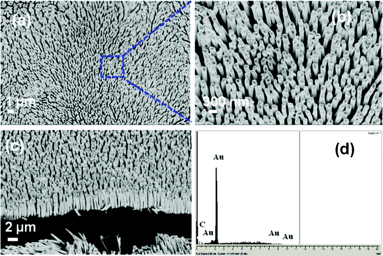
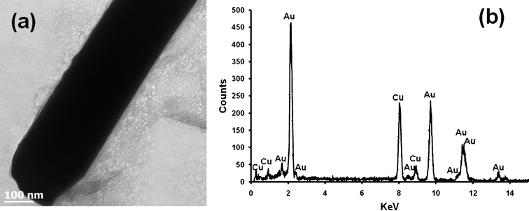
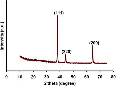
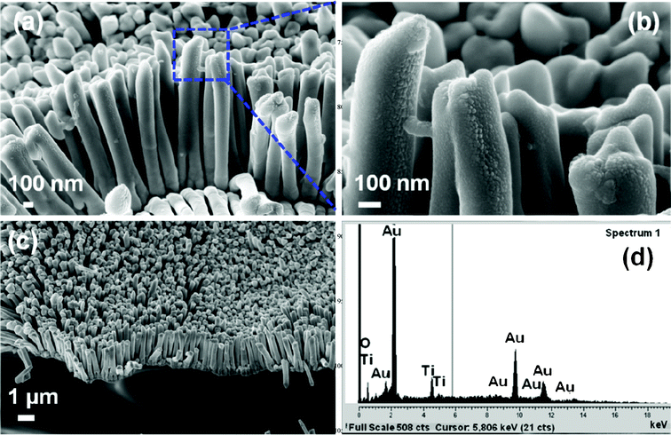
Fig. 1 shows the low (a) and high (b) magnification FESEM images of electrochemically synthesized Au nanowire arrays. Fig. 1 (a) illustrates a typical area (50 × 50 μm) of the nanostructures imaged by FESEM. The inter-wire distance was about 100–400 nm as is evident in Fig. 1 (b). Fig. 1 (c) shows that the average length of the Au nanowires was ∼3–5 μm and the diameter was ∼200 nm. The EDS spectrum in Fig. 1 (d) shows the elemental analysis of the nanowires which gives peaks for Au. The peak for carbon was generated from the carbon tape used in the sample holder during FESEM imaging. Fig. 2 shows a representative TEM micrograph of a Au nanowire from the array. This image confirms the nanowire diameter of ∼200 nm. Fig. 2 (b) shows the EDS data for the nanowire showing peaks for Au. The Cu peak is from the Cu grid. To examine the overall crystallinity of the nanowire arrays, the XRD pattern was collected and is shown in Fig. 3. The XRD data also confirm the face centered cubic structure of metallic gold.
Au–TiO2 core–shell nanowires
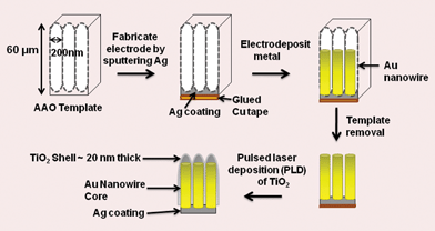
The Au–TiO2 core–shell nanowire arrays were fabricated by electrodeposition followed by pulsed laser deposition. The overall schematic of the synthesis is given in Fig. 4 above. The morphology and the composition of the synthesized Au–TiO2 core–shell nanowires were examined by FESEM and EDS. The images clearly illustrate the high alignment of the core–shell nanowire arrays on the substrate and that they are composed of Au and TiO2. Fig. 5 represents the FESEM images of Au–TiO2 core–shell nanowire arrays. Fig. 5 (b) reveals the high surface area available on the rough oxide surface, which will allow for more dye adsorption. Fig. 5 (c) shows a large area of the Au nanowire sample that is completely covered with TiO2 with the nanostructures standing vertically on the Ag film. This image is representative of the entire sample. The EDS data in Fig. 5 (d) show that the structure is made of Au, Ti and O without any detectable impurities. Fig. 6 (a) represents FESEM images from the top view of a Au–TiO2 core–shell nanowire array along with the corresponding EDS spectrum in Fig. 6 (b) taken from the bottom of one nanowire. These data show that the PLD technique is capable of coating even the bottom of the Au nanowires with the desired oxide material. This achievement was not possible with sputtering where only the tip of the wires was coated with Ti layers (images not shown). Fig. 6 (c) represents the uniform silver coating on the back of the Au–TiO2 nanowire array. The PLD approach was able to completely coat all exposed metal and result in a structure in which only TiO2 was exposed to the electrolyte solution of the DSSC. It has been reported for PLD that variation of the laser fluence, background gas pressure, deposition temperature or time has high impact on the thickness of the semiconductor layer.46–48 In our case, deposition time was ∼30 min. TEM imaging was used to examine the structure and the thickness of the TiO2 shell of core–shell nanowires after deposition of TiO2 using PLD. The results are shown in Fig. 7. Compared with the TEM image of bare Au nanowires given in Fig. 2, the TiO2 coated nanowire surface was very rough as shown in Fig. 7. A continuous shell of TiO2 is evident on all parts of the wire surface, with a thickness of ∼40 nm on the sides of the wires and slightly thicker at the tip. EDS analysis confirmed the presence of both gold and Ti. The HRTEM image in Fig. 8 (a) shows the edge of the core–shell nanowire where the TiO2 coating was ∼40 nm. The distance between two consecutive lattice fringes was calculated to be 3.52 Å which corresponds to the (101) plane of tetragonal anatase TiO2. The results are shown in the lattice resolved HRTEM image in Fig. 8 (b). The Au core is dark in color due to the higher density of the gold. The selected area electron diffraction (SAED) pattern in Fig. 8 (c) represents the concentric rings generated from the Au–TiO2 core–shell nanowires. The innermost rings are labeled with gold (right) and TiO2 anatase (left) indices. The concentric rings in the SAED pattern reveal the polycrystalline nature of the Au–TiO2 core–shell nanowire architectures. The synthesized structures served as the photoanode in dye sensitized solar cell devices. Ruthenium dye (N-535) was the sensitizer, and I−/I3− served as the redox couple. The J–V characteristics were measured under 100 mW cm−2 simulated sunlight. A schematic of the core–shell nanowire device is given in Fig. 9. We compared the current–voltage characteristics of Au–TiO2 nanowire solar cells with that of the TiO2 nanoparticle based DSSCs and TiCl4 surface passivated Au–TiO2 core–shell nanowire DSSCs. Treatment with 0.1 M TiCl4 (aq) was used in order to improve the surface area of the Au–TiO2 core–shell nanowire arrays. Surface treatment of the TiO2 photoanodes with a TiO2 precursor such as titanium tetrachloride TiCl449–53 and titanium isopropoxide Ti(OC3H7)454 has already been proven to enhance solar cell device performance by increasing photocurrent,55 enhancing surface area,56 improving electron transport,49 and improving anchoring of the dye.52 The morphology of the Au–TiO2 nanowires before and after the TiCl4 treatment was observed by FESEM imaging (data in the ESI, Fig. S3 and S4†). The J–V curves and data obtained upon illumination are given in Fig. 10 and Table 1 respectively. At first the devices were illuminated through the backside (Pt electrode) due to the presence of the opaque silver film and paint on the photoanode side. Although necessary for these devices with Ag film, backside illumination is detrimental because the redox couple can absorb some of the incident light before it reaches the photoanode.
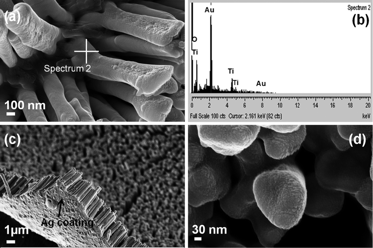 |
| | Fig. 6 FESEM images of Au–TiO2 core–shell nanowire arrays; (a) top view of array of nanowires, (b) EDS elementary analysis data of the as grown Au–TiO2 core–shell nanowire arrays giving peaks for Au, Ti and O), (c) array of Au–TiO2 core–shell nanowires showing the Ag film on which they are supported, (d) highly magnified top view of the Au–TiO2 core–shell nanowires. | |
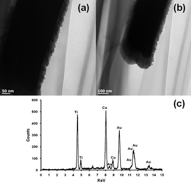 |
| | Fig. 7 (a) and (b) TEM images of Au–TiO2 core–shell nanowires, (c) EDS spectrum showing peaks for Au and Ti (copper is from the TEM support). PLD treatment was conducted for 30 min. | |
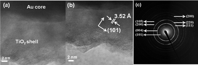 |
| | Fig. 8 (a) and (b) HRTEM images of the Au–TiO2 core–shell nanowire, (c) SAED pattern of the Au–TiO2 nanowires, with innermost rings labeled, left side indices for anatase TiO2 and right side indices for fcc Au. | |
 |
| | Fig. 9 Schematic of assembled backside illuminated Au–TiO2 nanowire DSSC or TiCl4 treated Au–TiO2 core–shell DSSC. | |
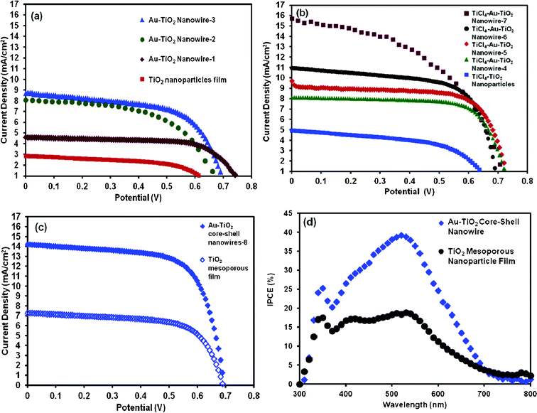 |
| | Fig. 10 (a) J–V curves of DSSCs fabricated with backside illuminated bare Au–TiO2 core–shell nanowire and TiO2 mesoporous nanoparticle film (b) J–V curves of backside illuminated TiCl4 treated Au–TiO2 core–shell nanowire and TiCl4 treated TiO2 mesoporous nanoparticle film DSSCs. Devices 2 and 7 were measured using a different solar simulator which had some light fluctuations that contributed to the low fill factor. (c) J–V curves of frontside illuminated Au–TiO2 core–shell nanowire and TiO2 mesoporous nanoparticle film DSSCs and, (d) IPCE spectra of DSSCs based on Au–TiO2 core–shell nanowire and TiO2 mesoporous nanoparticle film. | |
Table 1
J–V Characteristics of dye-sensitized Au–TiO2 core–shell nanowires, and TiCl4 treated Au–TiO2 core–shell nanowires DSSCs under 1 Sun
| Photoanode film type |
Type of illumination |
Approx. film thickness (μm) |
J
sc (mA cm−2) |
V
oc (V) |
FF (%) |
η (%) |
| Au–TiO2 core–shell nanowires-1 |
Backside |
3.0 |
4.6 |
0.78 |
66 |
2.3 |
| Au–TiO2 core–shell nanowires-2 |
Backside |
3.5 |
8.0 |
0.68 |
55 |
3.0 |
| Au–TiO2 core–shell nanowires-3 |
Backside |
3.5 |
8.7 |
0.71 |
59 |
3.7 |
| TiCl4 treated Au–TiO2 core–shell nanowires-4 |
Backside |
4.0 |
8.1 |
0.73 |
71 |
4.3 |
| TiCl4 treated Au–TiO2 core–shell nanowires-5 |
Backside |
4.5 |
9.7 |
0.74 |
69 |
4.7 |
| TiCl4 treated Au–TiO2 core–shell nanowires-6 |
Backside |
4.9 |
11.0 |
0.69 |
65 |
5.0 |
| TiCl4 treated Au-TiO2 core–shell nanowires-7 |
Backside |
4.9 |
15.7 |
0.73 |
49 |
5.6 |
| Au-TiO2 core–shell nanowires-8 |
Frontside |
4.2 |
14.2 |
0.69 |
67 |
6.7 |
| TiO2 mesoporous nanoparticles film |
Frontside |
4.0 |
7.3 |
0.69 |
65 |
3.3 |
| TiO2 mesoporous nanoparticles film |
Backside |
3.0 |
2.8 |
0.66 |
55 |
1.0 |
| TiCl4 treated TiO2 mesoporous nanoparticles film |
Backside |
4.0 |
4.9 |
0.67 |
53 |
1.7 |
In order to study the effect of a metal core inside the TiO2 shell on the photovoltaic performance of DSSCs, we compared the J–V data of several devices (Table 1). The 3 μm long Au–TiO2 core–shell nanowire device showed a Jsc and η of 4.6 mA cm−2 and 2.3% respectively, while the corresponding values for a 3 μm thick TiO2 mesoporous DSSC were 2.8 mA cm−2 and 1.06%. A higher Voc of the DSSC with Au–TiO2 core–shell device compared to that of the cell with TiO2 nanoparticles is in accordance with their Jsc values. A higher Jsc implies a faster electron transfer in the device, which favors an increased Voc for the Au–TiO2 core–shell device. The best efficiency and best fill factor (FF) of the 3.5 μm Au–TiO2 core–shell nanowire based devices were found to be 3.7% and 66.0% respectively. The results were obtained by applying only a ∼40 nm TiO2 layer which coated the entire core metal from top to bottom.
The ability of the gold core to transport electrons quickly out of the oxide and light scattering effects due to the gold metal core are both potential reasons for the improved efficiency in the core–shell DSSC devices. Additional devices were prepared and treated with TiCl4 prior to obtaining J–V curves. Efficiency for these devices ranged from 4.3–5.6%, with a trend of increasing efficiency with increasing length of the core–shell nanowires. Direct comparison of a 4 μm TiCl4 treated core–shell nanowire device and a 4 μm TiCl4 treated mesoporous nanoparticle device showed a 2.4 fold higher efficiency for the core–shell device. In order to check the effect of frontside illumination on device efficiency, we measured the J–V curves and their parameters by fabricating devices using a facile process involving dissolving the Ag film off the Au-TiO2 core–shell nanowire array and strongly adhering it onto FTO glass followed by sintering at high temperature. The fabrication process of the transparent photoanode is provided in Fig. S2 in the ESI† and an FESEM image of the Au–TiO2 core–shell nanostructure after the Ag layer removal is provided in Fig. S5 in the ESI.† The obtained solar conversion efficiency of 6.7% for the frontside illuminated DSSC is much higher than those of the backside illuminated DSSCs obtained in this study (5.6%). This difference is most likely due to better light transport through the frontside (FTO only) vs. the backside (platinized FTO and electrolyte). Dye desorption experiments showed similar dye loading among all devices tested (Table 2).
Table 2 Dye loading on photoanode films. After dye desorption with 0.1 M NaOH in ethanol, dye concentration was determined by absorbance at 310 nm followed by conversion to mol cm−2
| Photoanode type |
Dye loading mol cm−2 |
| TiO2 nanoparticle film (4.4 μm) |
3.9 × 10⁻⁶ |
| Au-TiO2 core–shell nanowires (4.5 μm) |
3.1 × 10⁻⁶ |
| TiCl4-treated core–shell nanowires (4.5 μm) |
3.3 × 10⁻⁶ |
Consequently, changes in dye loading cannot account for the enhanced efficiency for the core–shell device. Likely explanations include 1) improved electron transport due to the presence of the conducting core within the TiO2 film and 2) enhanced absorbance caused by optical effects of the metal nanowire array. Comparing mesoporous and core–shell devices, we observed a shift to higher Voc for the core–shell devices. This result indicates better electron transport most likely caused by the thin oxide film.57 The core–shell devices also exhibited higher FF than the mesoporous film devices. A 3 μm core–shell device had a FF of 66% while the 3 μm mesoporous device had a FF of 56% (Table 1). Similarly, a 4 μm TiCl4 treated core–shell device had a FF of 71% while the 4 μm TiCl4 treated mesoporous film device had a FF of 53%. The core–shell nanowires had a dye loading of 3.1 × 10⁻⁶ mol cm−2 when only the flat geometrical surface area (i.e. 0.24 cm2) was taken into consideration (Table 2). The TiCl4 treated Au–TiO2 core–shell nanowires had a dye loading of 3.3 × 10⁻⁶ mol cm−2. The amount of dye loading on the 4.5 μm long Au–TiO2 core–shell nanowire array and on the 4.5 μm TiCl4 treated Au–TiO2 core–shell nanowires was compared with a 4.4 μM thick film of mesoporous anatase. The mesoporous TiO2 film had a dye loading of 3.9 × 10⁻⁶ mol cm−2. The dye loading on the nanowire array was comparable to that on the mesoporous film. Previously reported dye loading values for DSSC range from 7.3 × 10⁻⁸ mol cm−2 to 4.8 × 10⁻⁵ mol cm−2.58–60 Our values fall within this broad range. However, the most important observation from our results is the relative loading of dye on the different structures. The nanowire arrays that we prepared had similar dye loading to a mesoporous film of comparable thickness, but the core–shell nanowire array devices had much greater photoconversion efficiency. Consequently, the enhanced efficiency of the core–shell nanowire devices is caused by a factor other than increased dye loading.
To further investigate the reasons for higher photocurrent for the solar cells based on Au–TiO2 core–shell nanowires, we measured the incident photon to current efficiency (IPCE) of mesoporous TiO2 nanoparticle and Au–TiO2 core–shell nanowire based solar cells. As shown in Fig. 10 (d), the IPCE for Au-TiO2 core–shell nanowire based device exhibited a peak of about 39.1% IPCE at 520 nm as well as a small shoulder at 400 nm. These peaks are in close agreement with the absorption spectrum for the N535 dye, which has local maxima at 400 and 533 nm, both corresponding to metal-to-ligand charge transfer transitions. The IPCE for the TiO2 nanoparticle based device exhibited a peak of about 18.3% at 520 nm as well as small shoulder at 400 nm. Notably, the IPCE profile of the Au–TiO2 core–shell nanowire based device was broadened and red shifted with respect to the TiO2 nanoparticle cell. The most likely reason for this broadened spectrum is light scattering by the Au nanowire array, resulting in enhanced light path length in the oxide/dye layer.61,62 The observed red shift for the Au–TiO2 core–shell nanowire cell will facilitate utilization of sunlight in the full spectrum range. The difference between these IPCE spectra (Fig. S6 in the ESI†) did not have a flat profile, indicating that there were wavelength dependent shifts in the IPCE spectrum due to the presence of gold in the Au–TiO2 nanowires. The maximum in the difference spectrum is near 520 nm, very close to the absorbance maximum of the dye. These results suggest possible coupling of the near field radiation with the absorbance dipole of the dye,63 which is no more than 30 nm from the metal surface. Resonance enhancement in absorbance cross sections near metal surfaces have been previously reported.64–67 In addition to the red shift, there is a small but reproducible peak near 620 nm for the structures with a gold core (see Fig. 10 (d) and S6†). Complete explanation of these optical features requires further in depth characterization of the optical properties of the core–shell nanowire arrays, a task that is currently underway.
Further improvements in the current densities and efficiencies could be obtained by growing longer nanowires with smaller diameter which would offer higher surface area and greater light harvesting. Nanowire aspect ratio is a huge factor to consider when it comes to providing control over the electron transport out of the anode. Growing longer wires with smaller diameter will enhance surface area and thus provide better light harvesting, which will substantially improve the current densities and efficiencies of cells made from nanowires58,68 A decrease in dark current causes the open circuit voltage to increase based on the relationship
| | |
V
oc = (kBT/q)ln(Iphoto/Idark + 1)
| (1) |
where
kB is the Boltzmann constant,
T is the temperature in Kelvin,
q is the charge, and
Idark and
Iphoto are the dark and photocurrents, respectively.
69 A decrease in semiconductor layer thickness will therefore result in an increase in the device efficiency. Reducing the semiconductor layer thickness will also allow for use of polycrystalline semiconductor materials with low minority carrier diffusion lengths. Thinner films will reduce the cost of devices due to reduced material, crystallinity, and purity demands and will open up room for using potentially inexpensive semiconductors with impurities and defects, for example CuO. The metal-metal
oxide core–shell
nanowire approach used in this study allowed the use of a thin (∼40 nm) semiconductor layer.
A promising new DSSC photoanode design was introduced where electrons created at the ∼40 nm thick semiconductor layer, radially diffuse to a metal core and are efficiently collected at the back contact. We have chosen gold as the material for the metallic core for proof of concept studies due to its high conductivity, thermal and chemical stability, and light focusing properties. Additional development of the preparation techniques will potentially lead to devices made from lower cost conductors such as copper or aluminum. The currently observed power conversion efficiency of 4.3% for a 4.0 μm TiCl4–Au–TiO2 core–shell nanowire cell was higher than the 2.38% efficiency observed for a 3.0 μm untreated Au–TiO2 core–shell nanowire DSSC. Furthermore, the efficiencies were only 1.8% and 1.1% for a 4 μm TiCl4–TiO2 mesoporous nanoparticle film DSSC and 3 μm untreated TiO2 mesoporous nanoparticle film DSSC, respectively. This evaluation confirms that our PLD grown Au–TiO2 core–shell nanowire based devices showed 2.2 to 2.4 times higher efficiency than the TiO2 mesoporous nanoparticle film DSSC of the same thickness. Recently reported data by Grätzel's group for TiO2 deposited by pulsed laser deposition directly onto an ITO substrate with no metal nanowires showed efficiencies of 3.1% (2 μm film), 4.9% (7 μm film) and 3.7% (13 μm film).42 The 2 μm PLD grown TiO2 film showed a 2.3 times lower efficiency as compared to their corresponding TiO2 mesoporous film DSSC of the same thickness. An important reason for the highly efficient mesoporous film DSSCs is their expertise in fabrication of high quality devices. In contrast, our work showed a 2.2 to 2.4 fold increase in the core–shell devices compared to the mesoporous devices. This difference underscores the importance of the metal core in improving the performance of devices based on PLD deposited TiO2. Our cell efficiency was limited by residual series resistance, most likely caused by imperfect contacts in our cell. Resolving these deficiencies should improve our efficiency well above the 6.7% we have already achieved. Furthermore, we utilized the N535 dye, which has a narrower absorbance spectrum compared to the C101 dye used by Grätzel's group. Another improvement we can make is increasing the length of our structures. Using 7 μm long PLD grown TiO2 structures on ITO, Grätzel's group achieved their maximum efficiency of 4.9%, indicating that efficiency improves as the thickness of the TiO2 increases as long as a maximum thickness is not exceeded. We can expect improvements by increasing the length of our structures and utilizing dyes that will have better coverage of the solar spectrum. The core–shell nanowire approach has considerable potential for making dramatic improvements in DSSC efficiency. Treatment of our devices with TiCl4 resulted in important improvements in efficiency (Table 1). Although previous reports have attributed such improvements to increased surface area and increased dye loading,56our dye desorption data (Table 2) did not show an increase in dye loading after TiCl4 treatmenmt. Furthermore, comparing J–V data for devices with and without TiCl4 treatment, no noticeable change in shunt current was observed. Samples without TiCl4 treatment exhibited minimal shunt current as evidenced by the flatness of the J–V curve extending close to Voc, This behavior suggests that little if any gold is directly exposed to the electrolyte. Based on these observations, the TiCl4 generated efficiency improvements recorded in this study are most likely due to improved light scattering.50
Conclusions
We synthesized novel Au–TiO2 core–shell nanoarchitectures and used them in dye sensitized solar cells. These core–shell structures showed very good performance in solar energy conversion. This improvement is likely the result of improved pathways for electron transport out of the anode after photoinduced charge injection as well as light focusing effects caused by the metal nanowire array. With an oxide thickness of 40 nm and a core conductor that spans the entire length of the core–shell structure, electrons injected into the oxide only have to travel around 40 nm before reaching a conductor. As a consequence, the use of fast redox couples like ferrocene may become possible with dye cells constructed from these core–shell nanostructures. The dye cells with core–shell photoanodes increased the current generation substantially as compared to the mesoporous nanoparticle film based DSSCs, thereby increasing the solar conversion efficiencies. Continuing studies aim to develop further improvements by increasing the length and surface area of TiO2, utilizing lower cost core materials, using dyes with broader spectral coverage and utilizing alternate redox couples.
Acknowledgements
This work was supported by the Louisiana Board of Regents, LEQSF (2007-12)-ENH-PKSFI-PRS-04, LEQSF(2011)-PFUND-269, and LEQSF (2008-13)-GF-19.
References
- B. Oregan and M. Gratzel, Nature, 1991, 353, 737 CrossRef CAS.
- N. Kopidakis, E. A. Schiff, N. G. Park, J. van de Lagemaat and A. J. Frank, J. Phys. Chem. B, 2000, 104, 3930 CrossRef CAS.
- L. M. Peter, Phys. Chem. Chem. Phys., 2007, 9, 2630 RSC.
- J. Nelson and R. E. Chandler, Coord. Chem. Rev., 2004, 248, 1181 CrossRef CAS.
- M. Law, L. E. Greene, J. C. Johnson, R. Saykally and P. D. Yang, Nat. Mater., 2005, 4, 455 CrossRef CAS.
- B. Tan and Y. Y. Wu, J. Phys. Chem. B, 2006, 110, 15932 CrossRef CAS.
- J. G. Chen, C. Y. Chen, C. G. Wu, C. Y. Lin, Y. H. Lai, C. C. Wang, H. W. Chen, R. Vittal and K. C. Ho, J. Mater. Chem., 2010, 20, 7201 RSC.
- Y. Xie, L. Zhou, C. Huang, H. Huang and J. Lu, Electrochim. Acta, 2008, 53, 3643 CrossRef CAS.
- S. Banerjee, S. K. Mohapatra, P. P. Das and M. Misra, Chem. Mater., 2008, 20, 6784 CrossRef CAS.
- Q. Wang, K. Zhu, N. R. Neale and A. J. Frank, Nano Lett., 2009, 9, 806 CrossRef CAS.
- S. K. Mohapatra, N. Kondamudi, S. Banerjee and M. Misra, Langmuir, 2008, 24, 11276 CrossRef CAS.
- S. G. Chen, M. Paulose, C. Ruan, G. K. Mor, O. K. Varghese, D. Kouzoudis and C. A. Grimes, J. Photochem. Photobiol., A, 2006, 177, 177 CrossRef CAS.
- D. Fang, K. L. Huang, S. Q. Liu and D. Y. Qin, Electrochem. Commun., 2009, 11, 901 CrossRef CAS.
- W. Zhu, G. Z. Wang, X. Hong, X. S. Shen, D. P. Li and X. Xie, Electrochim. Acta, 2009, 55, 480 CrossRef CAS.
- W. Zhu, G. Z. Wang, X. Hong and X. S. Shen, J. Phys. Chem. C, 2009, 113, 5450 CAS.
- H. Y. Zhang, T. H. Ji, Y. F. Liu and J. W. Cai, J. Phys. Chem. C, 2008, 112, 8604 CAS.
- H. Q. An, J. X. Li, J. Zhou, K. R. Li, B. L. Zhu and W. P. Huang, J. Mater. Chem., 2010, 20, 603 RSC.
- S. K. Mohapatra, S. Banerjee and M. Misra, Nanotechnology, 2008, 19, 155104 CrossRef.
- M. L. Wang, C. G. Huang, Y. G. Cao, Q. J. Yu, Z. H. Deng, Y. Liu, Z. Huang, J. Q. Huang, Q. F. Huang, W. Guo and J. K. Liang, J. Phys. D-Appl. Phys., 2009, 42 Search PubMed.
- M. Law, L. E. Greene, A. Radenovic, T. Kuykendall, J. Liphardt and P. D. Yang, J. Phys. Chem. B, 2006, 110, 22652 CrossRef CAS.
- P. V. Kamat, J. Phys. Chem. C, 2007, 111, 2834 CAS.
- S. Chappel, S. G. Chen and A. Zaban, Langmuir, 2002, 18, 3336 CrossRef CAS.
- A. B. F. Martinson, J. W. Elam, J. Liu, M. J. Pellin, T. J. Marks and J. T. Hupp, Nano Lett., 2008, 8, 2862 CrossRef CAS.
- Z. Z. Li, C. Rochford, F. J. Baca, J. W. Liu, J. Li and J. Wu, Nanoscale Res. Lett., 2010, 5, 1480 CrossRef CAS.
- K. M. Lee, C. W. Hu, H. W. Chen and K. C. Ho, Sol. Energy Mater. Sol. Cells, 2008, 92, 1628 CrossRef CAS.
- A. Kongkanand, R. M. Dominguez and P. V. Kamat, Nano Lett., 2007, 7, 676 CrossRef CAS.
- J. W. Liu, Y. T. Kuo, K. J. Klabunde, C. Rochford, J. Wu and J. Li, ACS Appl. Mater. Interfaces, 2009, 1, 1645 CAS.
- J. W. Liu, J. Li, A. Sedhain, J. Y. Lin and H. X. Jiang, J. Phys. Chem. C, 2008, 112, 17127 CAS.
- G. K. Mor, K. Shankar, M. Paulose, O. K. Varghese and C. A. Grimes, Nano Lett., 2006, 6, 215 CrossRef CAS.
- K. Zhu, T. B. Vinzant, N. R. Neale and A. J. Frank, Nano Lett., 2007, 7, 3739 CrossRef CAS.
- M. Gratzel, J. Photochem. Photobiol., A, 2004, 164, 3 CrossRef CAS.
- D. B. Kuang, S. Ito, B. Wenger, C. Klein, J. E. Moser, R. Humphry-Baker, S. M. Zakeeruddin and M. Gratzel, J. Am. Chem. Soc., 2006, 128, 4146 CrossRef CAS.
- M. Zukalova, A. Zukal, L. Kavan, M. K. Nazeeruddin, P. Liska and M. Gratzel, Nano Lett., 2005, 5, 1789 CrossRef CAS.
- M. Gratzel, Chem. Lett., 2005, 34, 8 CrossRef.
- P. Tammy, S. J. L. Chou and Guozhong Cao, Proceedings of SPIE–the international society for optical engineering, 2003, 5224, 5224 Search PubMed.
- E. Joanni, R. Savu, M. D. Goes, P. R. Bueno, J. N. de Freitas, A. F. Nogueira, E. Longo and J. A. Varela, Scr. Mater., 2007, 57, 277 CrossRef CAS.
- Z. X. Ye, H. D. Liu, I. Schultz, W. H. Wu, D. G. Naugle and I. Lyuksyutov, Nanotechnology, 2008, 19, 325303 CrossRef.
- H. W. Wang, C. F. Ting, M. K. Hung, C. H. Chiou, Y. L. Liu, Z. W. Liu, K. R. Ratinac and S. P. Ringer, Nanotechnology, 2009, 20, 055601 CrossRef.
- G. Sahu, S. W. Gordon and M. A. Tarr, RSC Adv., 2012, 2, 573 RSC.
- H. M. Bok, S. Kim, S. H. Yoo, S. K. Kim and S. Park, Langmuir, 2008, 24, 4168 CrossRef CAS.
- M. Rusop, T. Shirata, P. M. Sirimanne, T. Soga and T. Jimbo, Jpn. J. Appl. Phys., Part 1, 2003, 42, 4966 CrossRef CAS.
- F. Sauvage, F. Di Fonzo, A. L. Bassi, C. S. Casari, V. Russo, G. Divitini, C. Ducati, C. E. Bottani, P. Comte and M. Graetzel, Nano Lett., 2010, 10, 2562 CrossRef CAS.
- G. B. Wang, M. G. Fu, B. Lu, G. P. Du, L. Li, X. M. Qin and W. Z. Shi, Appl. Phys. A: Mater. Sci. Process., 2010, 100, 1169 CrossRef CAS.
- J. H. Noh, S. Lee, J. Y. Kim, J. K. Lee, H. S. Han, C. M. Cho, I. S. Cho, H. S. Jung and K. S. Hong, J. Phys. Chem. C, 2009, 113, 1083 CAS.
- B. Lee, D. K. Hwang, P. J. Guo, S. T. Ho, D. B. Buchholtz, C. Y. Wang and R. P. H. Chang, J. Phys. Chem. B, 2010, 114, 14582 CrossRef CAS.
- A. Bailini, F. Di Fonzo, M. Fusi, C. S. Casari, A. L. Bassi, V. Russo, A. Baserga and C. E. Bottani, Appl. Surf. Sci., 2007, 253, 8130 CrossRef CAS.
- A. Infortuna, A. S. Harvey and L. J. Gauckler, Adv. Funct. Mater., 2008, 18, 127 CrossRef CAS.
- F. Di Fonzo, C. S. Casari, V. Russo, M. F. Brunella, A. L. Bassi and C. E. Bottani, Nanotechnology, 2009, 20, 015604 CrossRef CAS.
- C. J. Barbe, F. Arendse, P. Comte, M. Jirousek, F. Lenzmann, V. Shklover and M. Gratzel, J. Am. Ceram. Soc., 1997, 80, 3157 CrossRef CAS.
- N. G. Park, G. Schlichthorl, J. van de Lagemaat, H. M. Cheong, A. Mascarenhas and A. J. Frank, J. Phys. Chem. B, 1999, 103, 3308 CrossRef CAS.
- M. K. Nazeeruddin, A. Kay, I. Rodicio, R. Humphrybaker, E. Muller, P. Liska, N. Vlachopoulos and M. Gratzel, J. Am. Chem. Soc., 1993, 115, 6382 CrossRef CAS.
- L. Y. Zeng, S. Y. Dai, K. J. Wang, X. Pan, C. W. Shi and L. Guo, Chin. Phys. Lett., 2004, 21, 1835 CrossRef CAS.
- P. Charoensirithavorn, Y. Ogomi, T. Sagawa, S. Hayase and S. Yoshikawaa, J. Electrochem. Soc., 2010, 157, B354 CrossRef CAS.
- D. Menzies, Y. B. Cheng, G. Simon and L. Spiccia, J. Australas. Ceram. Soc., 2003, 39, 108 CAS.
- B. C. O'Regan, J. R. Durrant, P. M. Sommeling and N. J. Bakker, J. Phys. Chem. C, 2007, 111, 14001 CAS.
- C. T. Yip, C. S. K. Mak, A. B. Djurisic, Y. F. Hsu and W. K. Chan, Appl. Phys. A: Mater. Sci. Process., 2008, 92, 589 CrossRef CAS.
- V. E. Ferry, M. A. Verschuuren, H. B. T. Li, E. Verhagen, R. J. Walters, R. E. I. Schropp, H. A. Atwater and A. Polman, Opt. Express, 2010, 18, A237 CrossRef CAS.
- J. B. Baxter and E. S. Aydil, Appl. Phys. Lett., 2005, 86, 053114 CrossRef.
- H. Hafez, J. H. Wu, Z. Lan, Q. H. Li, G. X. Xie, J. M. Lin, M. L. Huang, Y. F. Huang and M. S. Abdel-Mottaleb, Nanotechnology, 2010, 21, 415201 CrossRef.
- K. Keis, E. Magnusson, H. Lindstrom, S. E. Lindquist and A. Hagfeldt, Sol. Energy Mater. Sol. Cells, 2002, 73, 51 CrossRef.
- V. E. Ferry, J. N. Munday and H. A. Atwater, Adv. Mater., 2010, 22, 4794 CrossRef CAS.
- H. A. Atwater and A. Polman, Nat. Mater., 2010, 9, 205 CrossRef CAS.
- R. Bardhan, N. K. Grady, J. R. Cole, A. Joshi and N. J. Halas, ACS Nano, 2009, 3, 744 CrossRef CAS.
- H. A. Chen, J. L. Long, Y. H. Lin, C. J. Weng and H. N. Lin, J. Appl. Phys., 2011, 110, 054302 CrossRef.
- L. H. Qian, B. Das, Y. Li and Z. L. Yang, J. Mater. Chem., 2010, 20, 6891 RSC.
- L. Penninck, S. Mladenowski and K. Neyts, J. Opt., 2010, 12, 075001 CrossRef.
- E. Shafran, B. D. Mangum and J. M. Gerton, Phys. Rev. Lett., 2011, 107, 037403 CrossRef.
- Q. F. Zhang and G. Z. Cao, Nano Today, 2011, 6, 91 CrossRef CAS.
-
H. J. Moller,
Semiconductors for Solar Cells
, Artech House
, Boston,
1993,
64–75
Search PubMed.
|
| This journal is © The Royal Society of Chemistry 2012 |
Click here to see how this site uses Cookies. View our privacy policy here.