Color changeable OLEDs controlled by doping ratio and driving voltage with an anthracene derivative doped layer†
Ming-Yu
Teng
,
Qiu-Lei
Xu
,
Hong-Yan
Li
,
Lin
Wu
,
You-Xuan
Zheng
*,
Chen
Lin
* and
Leyong
Wang
State Key Laboratory of Coordination Chemistry, Nanjing National Laboratory of Microstructures, School of Chemistry and Chemical Engineering, Nanjing, 210093, P.R. China. E-mail: yxzheng@nju.edu.cn; linchen@nju.edu.cn
First published on 4th September 2012
Abstract
With 9,10-bis(3,3,3-triphenylprop-1-ynyl)anthracene (BTPYA) doped TPBi as an emissive layer, tunable OLED devices exhibited different emission colors (blue, near-white, green-yellow) controlled by the dopant ratio and driving voltage. The emissions were composed of the electrofluorescence of BTPYA, TPBi, and the electromer of BTPYA, an electroplex formed between BTPYA and TPBi.
The development of novel organic light-emitting diodes (OLEDs) for next-generation full-colour flat panel display has received increasing attention over the last two decades.1 It is now possible to produce OLEDs based on conjugated polymers,2 evaporated dyes,3 or the excimers and/or exciplexes4 of organic or polymer chromophores, which cover the whole visible spectrum. Many efforts have been made to improve the efficiency of these devices, for instance, by introducing a second transport layer to avoid quenching of the excitons at the cathode.5 However, much more research still has to be done to explain the exact nature of the physical states which give rise to electroluminescence (EL). Recently, several single-layer OLEDs have been reported based on the mixed emission of a blue emitter and an electromer or electroplex.6 For the electromer or electroplex, the energy of a hole-electron pair trapped by two neighbouring molecules should be lower than that of the singlet excited state of single molecule. As a result, indirect cross recombination of the hole and electron would lead to an emittance at a longer wavelength range compared with the fluorescence of non-doped organics.6a
Due to their outstanding photoluminescence and electroluminescence properties, anthracene derivatives have been used widely as blue emitting materials in OLEDs.7 We herein fabricated a series of devices utilizing TPBi (1,3,5-tri(1-phenyl-1H-benzo[d]imidazol-2-yl) phenyl) doped by 9,10-bis(3,3,3-triphenylprop-1-ynyl)anthracene (BTPYA)8 as an emitter layer. It is found that the electroluminescence spectra exhibited a broad blue light emission (450 nm) attributed to the electrofluorescence of BTPYA in a doping ratio of BTPYA in TPBi range from 50 to 20 wt% at low driving voltage (<10 V). It is interesting to note that with an increasing driving voltage (10–20 V), a new strong peak (∼560 nm) was generated due to the formation of an electroplex, and the devices gradually exhibited different emission colors ranging from blue and near-white, to green-yellow.
BTPYA was prepared smoothly via the Sonogashira cross-coupling reaction in a good yield (86%) using dibromoanthracene and prop-2-yne-1,1,1-triyltribenzene as the starting materials (Fig. S1†), according to published literature.8 The structure of BTPYA was further unambiguously determined by single-crystal X-ray diffraction (Fig. S1†, Table S1†, and Table S2†).
The absorption spectrum of BTPYA in CHCl3 was investigated (Fig. 1, green solid line). Strong absorption peaks appear at 234 and 272 nm due to the π→π* transition. There are three weak peaks at 391, 414, and 441 nm, respectively, in the visible absorption region. Three emission peaks of BTPYA in CHCl3 appear at 441, 468, and 499 nm. The emission peak in the solid state is observed at 488 nm with a weak shoulder peak at 508 nm, and it red-shifts about 40 nm compared to the photoluminescence in CHCl3. The PL spectra of BTPYA in different solvents were similar to each other suggesting that solvents with different polarities do not affect the emission greatly (Fig. 1).
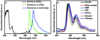 | ||
| Fig. 1 The UV-vis absorption and photoluminescence spectra of BTPYA in CHCl3 solution and in the solid state (a); the photoluminescence spectra of BTPYA in different solvents (b). | ||
The cyclic voltammogram of BTPYA was measured in CH2Cl2 using ferrocene as an internal standard. During the anodic scanning, BTPYA showed a reversible oxidation couple as two inflexions with a redox potential in the region of −2.0–2.0 V. On the basis of the potentials of the oxidation and reduction couples (Fig. S2†), the HOMO and LUMO energy levels of BTPYA were estimated to be −5.10 and −2.40 eV, respectively, with regard to the energy level of the ferrocene reference (4.8 eV below the vacuum level).9
To evaluate the EL character, BTPYA was utilized as an emitter in the fabrication of organic light-emitting devices. Initially, the simple device structure of ITO/NPB(N,N′-bis(naphthalen-1-yl)-N,N′-bis(phenyl)-benzidine) (40 nm)/BTPYA (50 nm)/TPBi (60 nm)/LiF (1 nm)/Al (100 nm) (device A) was fabricated (Fig. 2). The turn-on voltage of device A is 4.5 V with a maximum luminance, current efficiency (ηc), and power efficiency (ηp) of 2834 cd m−2, 0.99 cd A−1, and 0.37 lm W−1, respectively. Device A emits green-yellow light (the Commission Internationale de L'Eclairage (CIE) coordinates are x = 0.38, y = 0.44) with a highest peak at 567 nm (due to the BTPYA emission) and a weak shoulder at 380 nm (due to the TPBi emission).
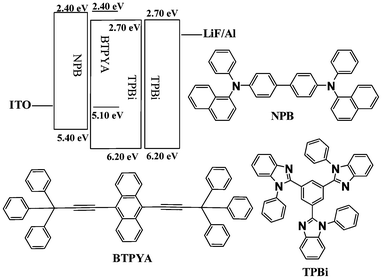 | ||
| Fig. 2 Energy level diagram of HOMO and LUMO levels (relative to vacuum level) for materials investigated in this work and their molecular structures. | ||
Then we fabricated several devices with BTPYA (x wt%):TPBi as a single emissive layer. By adjusting the doping ratio of BTPYA in TPBi, seven devices with doping ratios of BTPYA ranging from 90 to 20 wt% (devices B–H) were fabricated. The brightness versus voltage (V−B), power efficiency (ηp) as a function of current density (J), and current efficiency (ηc) as a function of current density (J) curves for all the devices are listed in Fig. S3† and some important performance data are listed in Table 1.
| Device | Configuration (BTPYA wt%) | V t a (V) | L max b (cd m−2, V) | η p,max c (lm W−1, V) | η c,max d (cd A−1, V) | ||||||||||||||||||||||||||||||||||||||||||||||||||||||||||||||||||||||||||||||||||||||||||||||
|---|---|---|---|---|---|---|---|---|---|---|---|---|---|---|---|---|---|---|---|---|---|---|---|---|---|---|---|---|---|---|---|---|---|---|---|---|---|---|---|---|---|---|---|---|---|---|---|---|---|---|---|---|---|---|---|---|---|---|---|---|---|---|---|---|---|---|---|---|---|---|---|---|---|---|---|---|---|---|---|---|---|---|---|---|---|---|---|---|---|---|---|---|---|---|---|---|---|---|---|
| a V t is the turn-on voltage (V). b L max is the maximum luminance (1 cd m−2). c η p,max is the maximum power efficiency. d η c,max is the maximum power efficiency. | |||||||||||||||||||||||||||||||||||||||||||||||||||||||||||||||||||||||||||||||||||||||||||||||||||
| A | 100 | 4.5 | 2834, 10.9 | 0.37, 8.1 | 0.99, 8.3 | ||||||||||||||||||||||||||||||||||||||||||||||||||||||||||||||||||||||||||||||||||||||||||||||
| B | 90 | 4.0 | 2923, 12.3 | 1.31, 5.9 | 2.90, 7.5 | ||||||||||||||||||||||||||||||||||||||||||||||||||||||||||||||||||||||||||||||||||||||||||||||
| C | 80 | 4.0 | 1368, 10.5 | 0.96, 6.5 | 2.01, 7.1 | ||||||||||||||||||||||||||||||||||||||||||||||||||||||||||||||||||||||||||||||||||||||||||||||
| D | 60 | 3.8 | 3616, 12.3 | 1.72, 5.3 | 3.23, 6.6 | ||||||||||||||||||||||||||||||||||||||||||||||||||||||||||||||||||||||||||||||||||||||||||||||
| E | 50 | 3.9 | 2768, 12.2 | 0.91, 5.4 | 1.69, 6.3 | ||||||||||||||||||||||||||||||||||||||||||||||||||||||||||||||||||||||||||||||||||||||||||||||
| F | 40 | 4.4 | 1610, 13.9 | 0.24, 9.7 | 0.76, 9.7 | ||||||||||||||||||||||||||||||||||||||||||||||||||||||||||||||||||||||||||||||||||||||||||||||
| G | 30 | 4.5 | 1750, 14.0 | 0.18, 9.7 | 0.58, 10.3 | ||||||||||||||||||||||||||||||||||||||||||||||||||||||||||||||||||||||||||||||||||||||||||||||
| H | 20 | 6.8 | 842, 15.0 | 0.06, 8.1 | 0.19, 10.7 | ||||||||||||||||||||||||||||||||||||||||||||||||||||||||||||||||||||||||||||||||||||||||||||||
Devices B–D were constructed by changing the doping ratio of BTPYA in TPBi from 90 to 60 wt%. The TPBi host causes a lower turn-on voltage. Device D (60 wt% dopant) shows the highest luminance of 3616 cd m−2, while devices B (90 wt% dopant) and C (80 wt% dopant) gave a luminance of 2923 and 1368 cd m−2, respectively. The normalized EL spectra of devices A–D at a relatively low driving voltage are exhibited in Fig. 3, showing that the contribution of the emission in the longer wavelength range dramtically decreases, and the strength of the emission from BTPYA increases as the doping ratio of the BTPYA decreases.
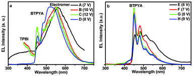 | ||
| Fig. 3 EL spectra of devices A–D (a) and E–H (b) at different voltages. | ||
As can be seen from the CIE coordinates of the devices at a low driving voltage (6–14 V, Fig. S3†), device A's color at 7 V (x = 0.38, y = 0.44) is almost yellowish green exhibiting the main emission in the longer wavelength range. With a decrease of the doping ratio of BTPYA, the emission from BTPYA is strengthened and the colors of emitted light from devices B–D change first to green and then to cyan. Meanwhile, with increasing the voltage, the colors of devices B–D change slightly (Fig. S4†).
As discovered by the performance data, the decreasing doping ratio of BTPYA results in a higher turn-on voltage, weaker maximum luminance, current efficiency (ηc) and power efficiency (ηp). It's much interesting that when the doping ratio of BTPYA is further decreased to 50 wt%, devices E–H emit blue light due to the emission of BTPYA at low driving voltage. The normalized EL spectra of devices E–H at low driving voltages are exhibited in Fig. 3 (b). It appears that there are aggregates of the dopant and intercalated domains (akin to bulk organic heteroconjunctions) in our system. From Table 1 it can be observed that the devices with 50–60 wt% dopant concentrations have the lowest driving voltages. The increase or decrease of the dopant concentration causes an increase of the driving voltage and a decrease in device efficiency.
Surprisingly, with an increase in driving voltage, an emission peak at about 560 nm was generated and the intensity also increased. Additionally, the weak TPBi emission peak at 380 nm was also regenerated. The EL spectra for device E (50% dopant) at a driving voltage range from 6 to 20 V are shown in Fig. 4. The peaks at 450 and 480 nm are attributed to BTPYA, and the emission at 380 nm is caused by TPBi.
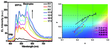 | ||
| Fig. 4 EL spectra of device E with increasing voltage (left) and the CIE (x, y) chromaticity diagrams of devices E–H (right). | ||
Fig. 5 shows the PL spectra of the films with different doping ratios of BTPYA in TPBi. They are very similar to those of the solid state. However, for devices A–H, there are new emissions with longer wavelengths at around 560 nm. An excimer peak at 505 nm will emerge with an increase in the doping ratio. Meanwhile the emission peak at 450 nm will decline, but the emission peak at about 560 nm is never observed in the PL spectra. According to recent publications,6 these emissions should be generated from the electromer of BTPYA and electroplex between BTPYA and TPBi. Regardless of whether the excited energy is light or electricity, excimer and exciplex emissions can be obtained. However, electromer and electroplex emissions may occur in the presence of a high electric field and never in the PL spectra.6,10 For device A, the emissive layer is only BTPYA, and it is easy to form the electromer in the electric field. When BTPYA disperses in TPBi (>50 wt%, devices B–D) in higher dopant concentrations, the percentage of electromer decreases and the emission of BTPYA increases with the decreasing of dopant concentration (Fig. 4a). When the concentration of BTPYA is lower than 50 wt% (devices E–H), only the BTPYA emission can be observed at a relatively low driving voltage (Fig. 4b). At higher voltages, the electroplex can be formed between BTPYA and TPBi due to the excess of TPBi.
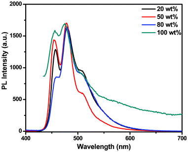 | ||
| Fig. 5 PL spectra of BTPYA in the TPBi film (BTPYA wt%). | ||
The energy levels and dynamic processes of BTPYA, TPBi and electromer/electroplex emissions of the device ITO/NPB/BTPYA:TPBi/TPBi/LiF/Al are demostrated in Fig. 6. The energy barriers of the HOMO levels between NPB and BTPYA, and NPB and TPBi are estimated to be 0.30 eV and 0.80 eV, respectively. The energy barrier of LUMO levels between BTPYA and TPBi is estimated to be 0.30 eV. In high dopant concentrations, the electromer can be regarded as a pair of statistically independent BTPYA molecules, in which one has an excess electron (BTPYA−), while the other has a hole (BTPYA+). The energy of such a hole-electron pair trapped by two neighboring molecules should be lower than that of the singlet excited state of a single molecule. As a result, direct cross recombination of the hole and the electron would lead to an emission at a longer wavelength range compared to the emission of BTPYA. The electroplex is a result of a charge transfer interaction between the excited/ground state of the donor and the ground/excited state of the acceptor. Under electrical excitation, the electroplex should be formed by the confinement of the carriers injected from the opposite electrodes between electron donor and acceptor molecules. For example, in the devices ITO/NPB/BTPYA:TPBi/TPBi/LiF/Al, the electroplex is a result of a charge transfer interaction between the excited ground state of the TPBi and the ground excited state of the BTPYA. The energy barriers between BTPYA and TPBi are estimated to be ΔHOMO = 1.10 eV and ΔLUMO = 0.30 eV. When a positive voltage is applied to the ITO electrode, holes are injected from ITO and NPB into the HOMO of BTPYA, and electrons are simultaneously injected to the LUMO of TPBi. Holes and electrons are able to transport from NPB and TPBi to the HOMO levels of BTPYA and the LUMO levels of BTPYA and TPBi through a hopping mechanism under a low driving voltage, of which the combination is contributed to by BTPYA emission. The higher energy barrier between the HOMO of BTPYA and TPBi prevents injection of the holes into the pure TPBi layer. Thus, when forward bias is applied, holes will accumulate at the HOMO of the BTPYA layer. When the injected holes and electrons encounter each other at the doped layer and interface of BTPYA and TPBi, the electron and hole recombine between the two molecules (D+ and D−) to form the BTPYA:TPBi electroplex.11 As the driving voltage increases, some holes and electrons will accumulate at the HOMO and LUMO levels of TPBi, and most of accumulating electrons at the LUMO of TPBi can recombine with the holes at the HOMO level of BTPYA, resulting in the enhancement of electroplex emission. A small amount of accumulated electrons at the LUMO of TPBi could recombine with the holes at the HOMO level of itself, leading to a TPBi emission. The electroplex emitting peak is red-shifted relative to the emissions of BTPYA and TPBi. In addition, the electroplex emission is shifted to a lower energy due to the Stokes shift effect with respect to the HOMO (BTPYA)–LUMO (TPBi) difference for this transition.12
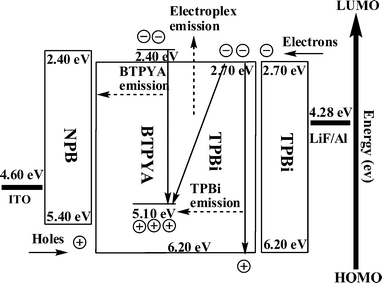 | ||
| Fig. 6 The plausible distributions of the dynamic process of electroplex emission. | ||
The colors of devices E (x = 0.23, y = 0.35) and F (x = 0.18, y = 0.26) at 6 V are near-sky-blue and blue, respectively, exhibiting main BTPYA emission. With an increase of the driving voltage, it is clear that the strength of the emission from the electroplex becomes stonger, which results in a color change of the emission light of device E from blue to yellowish-green (x = 0.32, y = 0.41). As shown in the EL spectra of device E (Fig. 4), the electroplex peak becomes the main emission peak at 14 V. For device F, the emission color of light changes from blue to sky blue (x = 0.24, y = 0.32) at 13 V.
Upon further decreasing the doping ratio of BTPYA to 30 and 20 wt%, respectively, the color of the emission light of devices G (x = 0.19, y = 0.22) and H (x = 0.19, y = 0.27) at 8 V is almost blue due to exhibiting only the BTPYA emission. For device G, the electroplex peak is generated at 10 V (x = 0.19, y = 0.22), and the relative intensity of the BTPYA peak increases with an increase in voltage. At 20 V, the color of the emission light of device G changes to sky blue (x = 0.25, y = 0.30). The color of the emission light of device H changes to sky blue (x = 0.23, y = 0.33) at 12 V, and then to cyan (x = 0.27, y = 0.38) at 20 V due to the higher contribution of the electroplex emission. It is noticable that this process is irreversible, e.g. the emission color generated at a high driving voltage can be retained without the color change after decreasing the voltage. The result indicates that the driving voltage benefits from the formation of a stable electromer and electroplex.
In conclusion, doping ratio and voltage tunable OLEDs were obtained based on doped TPBi with BTPYA as a single emitting layer. The device colors depend on the EL emissions from BTPYA, the electromer and the electroplex. The ratio among these emissions can be controlled by the doping ratio of BTPYA and a bias voltage applied to the devices, leading to doping ratio and voltage controlled color light sources. The color of emission light tunability as a function of the doping ratio and driving voltage could be utilized for novel voltage sensors and different color emission OLEDs. Further work will be undertaken in order to improve device efficiency, luminance, and to achieve a “pure” white emission.
We gratefully acknowledge the financial support of NSFC (20602017, 20971067, 21021062 and 21072093), the Natural Science Foundation of Jiangsu (BK2011551), the National Basic Research Program of China (2011CB808704), and the Doctoral Fund of the Ministry of Education of China (20090091110017). This research was also supported by the fundamental research funds for central universities.
References
- (a) C. W. Tang and S. A. Vanslyke, Appl. Phys. Lett., 1987, 5, 913–915 CrossRef; (b) J. H. Burroughes, D. D. C. Bradley, A. R. Broun, R. N. Marks, K. Mackay, R. H. Friend, P. L. Burn and A. B. Holmes, Nature, 1990, 347, 539–541 CrossRef CAS; (c) J. Kido, W. Ikeda, M. Kimura, K. Nagai, K. Okuyama, Y. You, A. Shoustikov, S. Sibley, M. E. Thompson and S. R. Forrest, Nature, 1998, 395, 151–154 CrossRef; (d) G. Sakamoto, C. Adachi, T. Koyama, Y. Taniguchi, C. D. Merritt, H. Murata and Z. H. Kafafi, Appl. Phys. Lett., 1999, 75, 766–768 CrossRef CAS; (e) Q. J. Sun, B. H. Fan, Z. A. Tan, C. H. Yang and Y. F. Li, Appl. Phys. Lett., 2006, 88, 163510–163512 CrossRef; (f) Z. Y. Xie, J. S. Huang, C. N. Li, S. Y. Liu, Y. Wang, Y. Q. Li and J. C. Shen, Appl. Phys. Lett., 1999, 74, 641–643 CrossRef CAS; (g) Y. H. Kim, D. C. Shin, S. H. Kim, C. H. Ko, H. S. Yu, Y. D. Chae and S. K. Kwon, Adv. Mater., 2001, 13, 1690–1393 CrossRef CAS; (h) C. W. Ko and Y. T. Tao, Appl. Phys. Lett., 2001, 79, 4234–4236 CrossRef CAS; (i) C.-H. Kim and J. Shinar, Appl. Phys. Lett., 2002, 80, 2202–2204 Search PubMed; (j) B. W. D’Andrade, M. E. Thompson and S. R. Forrest, Adv. Mater., 2002, 14, 147–151 CrossRef; (k) C. Pérez-Bolívar, S. Takizawa, G. Nishimura, V. A. Montes and P. Anzenbacher, Chem.–Eur. J., 2011, 17, 9076–9082 CrossRef; (l) J. Kido, H. Shionoya and K. Nagai, Appl. Phys. Lett., 1995, 67, 2281–2283 CrossRef CAS; (m) M. Granstrom and O. Ingans, Appl. Phys. Lett., 1996, 68, 147–149 CrossRef; (n) R. S. Deshpande, V. Bulović and S. R. Forrest, Appl. Phys. Lett., 1999, 75, 888–890 CrossRef CAS; (o) Y. Liu, J. H. Guo, H. D. Zhang and Y. Wang, Angew. Chem., Int. Ed., 2002, 41, 182–184 CrossRef CAS; (p) M. Mazzeo, D. Pisignano, F. Della Sala, J. Thompson, R. I. R. Blyth, G. Gigli, R. Cingolani, G. Sotgiu and J. Barbarella, Appl. Phys. Lett., 2003, 82, 334–336 CrossRef CAS; (q) H. Kanno, Y. Sun and S. R. Forrest, Appl. Phys. Lett., 2005, 86, 263502–263504 CrossRef.
- (a) M. R. Andersson, M. Berggren, O. Inganäs, G. Gustafsson, J. C. Gustafsson-Carlberg, D. Selse, T. Hjertberg and O. Wennerström, Macromolecules, 1995, 28, 7525–7529 CrossRef CAS; (b) M. Berggren, O. Inganäs, G. Gustafsson, J. Rasmusson, M. R. Andersson, T. Hjertberg and O. Wennerström, Nature, 1994, 372, 444–446 CrossRef CAS.
- (a) J. Kido, M. Kimura and K. Nagai, Science, 1995, 267, 1332–1334 CAS; (b) T. Tsutsui, E. Aminaka, C. P. Lin and D.-U. Kim, Philos. Trans. R. Soc. London, Ser. A, 1997, 355, 801–824 CrossRef CAS.
- (a) B. W. D'Andrade, J. Brooks, V. Advamovich, M. E. Thompson and S. R. Forrest, Adv. Mater., 2002, 14, 1032–1036 CrossRef CAS; (b) C. L. Chao and S. A. Chen, Appl. Phys. Lett., 1997, 73, 426–428 CrossRef; (c) M. Mazzeo, D. Pisignano, F. D. Sala, J. Thompson, R. I. R. Blyth, G. Gigli, G. Sotgiu and G. Barbarella, Appl. Phys. Lett., 2003, 82, 334–336 CrossRef CAS; (d) L. C. Palilis, A. J. Mäkinen, M. Uchida and Z. H. Kafafi, Appl. Phys. Lett., 2003, 82, 2209–2211 CrossRef CAS; (e) G. Cheng, Y. Zhang, Y. Zhao, S. Liu, Z. Xie, H. Xia, M. Hanif and Y. Ma, Appl. Phys. Lett., 2005, 87, 013506–013508 CrossRef; (f) M. Li, W. Li, L. Chen, Z. Kong, B. Chu, B. Li, Z. Hu and Z. Zhang, Appl. Phys. Lett., 2006, 88, 091108–091110 CrossRef.
- C. Adachi, T. Tsutsui and S. Saito, Appl. Phys. Lett., 1990, 56, 799–801 CrossRef CAS.
- (a) T. Granlund, L. A. A. Pettersson, M. R. Anderson and O. Inganäs, J. Appl. Phys., 1997, 81, 8097–8104 CrossRef CAS; (b) J. Rommens, A. Vaes, M. Van der Auweraer, F. C. De Schryver, H. Bässler, H. Vestweber and J. Pommerehne, J. Appl. Phys., 1998, 84, 4484–4494 CrossRef; (c) J. Kalinowski, G. Giro, M. Cocchi, V. Fattori and P. Di Marco, Appl. Phys. Lett., 2000, 76, 2352–2354 CrossRef CAS; (d) J. Y. Li, D. Liu, C. Ma, O. Lengyel, C. –S. Lee, C. –H. Tung and S.-T. Lee, Adv. Mater., 2004, 16, 1538–1541 CrossRef CAS; (e) Y. Liu, M. Nishiura, Y. Wang and Z. Hou, J. Am. Chem. Soc., 2006, 128, 5592–5593 CrossRef CAS.
- (a) J. Shi and C. W. Tang, Appl. Phys. Lett., 2002, 80, 3201–3213 CrossRef CAS; (b) Y. Kan, L. Wang, L. Duan, Y. Hu, G. Wu and Y. Qiu, Appl. Phys. Lett., 2004, 84, 1513–1515 CrossRef CAS; (c) T. H. Liu, Y. S. Wu, M. T. Lee, H. H. Chen, C. H. Liao and C. H. Chen, Appl. Phys. Lett., 2004, 85, 4304–4306 CrossRef CAS; (d) M. T. Lee, H. H. Chen, C. H. Liao, C. H. Tsai and C. H. Chen, Appl. Phys. Lett., 2004, 85, 3301–3303 CrossRef CAS; (e) Y. H. Kim, D. C. Shin, S. H. Kim, C. H. Ko, H. S. Yu, Y. S. Chae and S. K. Kwon, Adv. Mater., 2001, 13, 1690–1693 CrossRef CAS; (f) Y. H. Kim, H. C. Jeong, S. H. Kim, K. Yang and S. K. Kwon, Adv. Funct. Mater., 2005, 15, 1799–1805 CrossRef CAS; (g) W. J. Shen, R. Dodda, C. C. Wu, F. L. Wu, T. H. Liu, H. H. Chen, C. H. Chen and C. F. Shu, Chem. Mater., 2004, 16, 930–934 CrossRef CAS; (h) K. Danel, T. H. Huang, J. T. Lin, Y. T. Tao and C. H. Chuen, Chem. Mater., 2002, 14, 3860–3865 CrossRef CAS; (i) P.-I. Shih, C.-Y. Chuang, C.-H. Chien, E. W.-G. Diau and C.-F. Shu, Adv. Funct. Mater., 2007, 17, 3141–3146 CrossRef CAS; (j) C.-J. Zheng, W.-M. Zhao, Z.-Q. Wang, D. Huang, J. Ye, X.-M. Ou, Z.-H. Zhang, X.-S. Lee and S.-T. Lee, J. Mater. Chem., 2010, 20, 1560–1566 RSC.
- J. E. Nuñez, A. Natarajan, S. I. Khan and M. Garcia-Garibay, Org. Lett., 2007, 9, 3559–3561 CrossRef.
- (a) M. Thelakkat and H. W. Schmidt, Adv. Mater., 1998, 10, 219–223 CrossRef CAS; (b) R. S. Ashraf, M. Shahid, E. Klemm, M. Al-Ibrahim and S. Sensfuss, Macromol. Rapid Commun., 2006, 27, 1454–1459 CrossRef CAS.
- (a) C. L. Chao and S. A. Chen, Appl. Phys. Lett., 1998, 72, 636–638 CrossRef; (b) G. Giro, M. Cocchi, J. Kalinowski, P. Di Marco and V. Fattori, Chem. Phys. Lett., 2000, 318, 137–141 CrossRef CAS; (c) X. Z. Jiang, R. A. Register, K. A. Killeen, M. E. Thompson, F. Pschenitzka, T. R. Hebner and J. C. Sturm, J. Appl. Phys., 2002, 91, 6717–6724 CrossRef CAS; (d) Z. M. Zhang, G. W. Li, Y. G. Ma and J. C. Shen, Mater. Chem. Phys., 2003, 82, 613–617 CrossRef CAS; (e) Y. M. Wang, F. Teng, Z. Xu, Y. B. Hou, S. Y. Yang, L. Qian, T. Zhang and D. A. Liu, Appl. Surf. Sci., 2004, 236, 251–255 CrossRef CAS.
- (a) J. Kalinowski, M. Cocchi and P. Marco, J. Phys. D: Appl. Phys., 2000, 33, 2379–2387 CrossRef CAS; (b) D. Virgili, M. Cocchi, V. Fattori, C. Sabatini, J. Kalinowski and J. A. G. Williams, Chem. Phys. Lett., 2006, 433, 145–149 CrossRef CAS; (c) H. Zhu, Z. Xu, F. Zhang, S. Zhao and D. Song, Appl. Surf. Sci., 2008, 254, 5511–5513 CrossRef CAS.
- A. Yildiz, F. Dagdelen, S. Acar, S. B. Lisesivdin, M. Kasap, Y. Aydogdu and M. Bosi, Acta Phys. Pol., A, 2008, 113, 731–739 CAS.
Footnote |
| † Electronic Supplementary Information (ESI) available: experimental details, crystallographlic data, and cyclovoltammetry (CV) diagram of BTPYA; preparation and characteristics of devices. |
| This journal is © The Royal Society of Chemistry 2012 |
