DOI:
10.1039/C2RA21065G
(Paper)
RSC Adv., 2012,
2, 10222-10230
Photocatalytic properties of semiconductor SnO2/CdS heterostructure nanocrystals†
Received
29th May 2012
, Accepted 18th August 2012
First published on 22nd August 2012
Abstract
Here we report the photocatalytic properties of semiconductor SnO2/CdS heterostructure nanocrystals. A type-II SnO2/CdS heterostructure has been synthesized from a single-source precursor and its structure was determined using XRD, HRTEM, elemental mapping and line scan EDAX analysis. A time resolved spectroscopic study revealed the effective charge separation in this heterostructure and the mechanism of charge separation was proposed using a schematic model. It is important to mention that the conductivity was found to be lower in the SnO2/CdS heterostructure compared to uncoated SnO2 nanorods due to efficient charge separation. The efficient charge separation in the SnO2/CdS heterostructure revealed its higher photocatalytic activity and the photocatalytic degradation of Congo red dye was found to be 97% and 20% for the SnO2/CdS heterostructure and SnO2 respectively under UV light irradiation.
1. Introduction
Significant progress has been made in recent years in designing and understanding the physical properties of semiconductor heterostructure nanomaterials because of their potential application in optoelectronic devices.1 Heterostructures of two different band gap semiconductors create type II heterojunction nanostructures. By tuning the energy levels of the valence and conduction bands of the semiconductors, spatial separation of charge carriers (excitons) occurs upon photoexcitation. There is a report on charge transfer dynamics of type II semiconductor QDs.2 There have been also several reports on heterostructure semiconductor nanocrystals such as, CdTe/CdSe,3 CdSe/ZnS,4,5 CdSe/CdS,6,7 ZnO/ZnS,8,9 TiO2/CdS,10 SnO2/CdS11–15 and ZnO/CdS16,17etc. Bawendi and co-workers3 have synthesized CdSe/ZnTe and CdTe/CdSe using chemical methods. Chen and co-workers18 have reported spatial separation of charge carriers by changing the size of the core and shell in CdSe/ZnTe. Banin and co-workers19 also reported the photophysical properties of ZnSe QDs within CdS nanorods and demonstrated charge separation.
Photocatalytic degradation of organic pollutants in water and air using semiconductors such as TiO2, ZnO, SnO2etc. has attracted extensive attention in the past two decades.20–22 Serpone et al. recently gave an overview on the past, present and future outlook of semiconductor photocatalysis.23 A recent review by Kumar et al. demonstrated the results and mechanisms of interfacial charge carrier transfer dynamics in TiO2 photocatalysis under UV/visible light.24 Tsang et al. reported the photocatalytic activity of ZnO nanocrystals with varying shape and size.25 Previous studies have proved that such semiconductors can degrade most kinds of persistent organic pollutants such as detergents, dyes, pesticides and volatile organic compounds under UV-irradiation. However, the fast recombination rate of the photogenerated electron–hole pairs hinders the commercialization of this technology.26 Thus, it is of great interest to researchers to improve the photocatalytic activity of semiconductors for the degradation of organic compounds in water and air. Recently, it was reported that semiconductor heterostructure nanomaterials may increase the photocatalytic efficiency by increasing the charge separation and extending the photo-responding range. There are a number of studies related to the photocatalytic activity of semiconductor heterostructure photocatalysts such as TiO2/CeO2,27 TiO2/SnO2,28,29 ZnO/SnO2,30--32 TiO2/ZnO,33–35 TiO2/CdS,36 ZnO/CdS37etc. Kim et al. found enhanced photocatalytic activity in TiO2/CdS heterostructures compared to TiO2 nanocrystals.36 Kundu et al. synthesized ZnO/CdS heterostructures and found higher photocatalytic activity in the heterostructures due to efficient charge separation.37 To the best of our knowledge, there is no report on the photocatalytic activity of SnO2/CdS heterostructures in the literature.
It is to be noted that the SnO2/CdS heterostructure is an important type-II type material in which the lower band gap material (CdS) is deposited around a core of SnO2 which has a wider band gap.11 Thus, the photogenerated carrier (electron) is predominantly confined to the core and the other (hole) is located in the shell. Relatively little attention has been paid to the fabrication of SnO2/CdS type II heterostructures, even though this material has been shown to have potential for making optoelectronic devices15 and gas sensors.11 Methods previously developed for the synthesis of SnO2/CdS include sonochemical synthesis,11 solution synthesis,15,12 dip coating method13 and colloidal approach.14 Generally, double source precursors have been used for making this type of heterostructure material. In the present study, a facile synthetic method for preparing a type-II SnO2/CdS heterostructure using a cadmium thiobenzoate complex as a single-source precursor for CdS is reported.
In the present study, we have used tetragonal SnO2 with lattice parameters a = 4.735, c = 3.175 and cubic CdS with lattice parameter a = 5.816. The lattice mismatching during the formation of type-II SnO2/CdS heterostructure may influence the optical, electrical and photocatalytic properties. Here, we used cadmium thiobenzoate complex as a single source precursor for CdS and deposited it on the surface of SnO2 nanorods using a hydrothermal method.38 The lattice strain and lattice parameters of SnO2 and the SnO2/CdS heterostructure were measured by X-ray diffraction study. Transmission electron microscopy (TEM), HRTEM and elemental mapping analysis were carried out to confirm the formation of the SnO2/CdS heterostructure. I–V characteristics of the heterostructure were found to be asymmetric and non-linear for the forward direction of applied voltage, indicating the formation of a Schottky barrier in the heterostructure. Time resolved and electrical analysis demonstrated the efficient charge separation in the SnO2/CdS heterostructure. The photocatalytic activity of this SnO2/CdS heterostructure has also been investigated.
2. Experimental section
2.1. Synthesis of cadmium thiobenzoate complex
1.0 mmol (0.286 g) of Na2CO3·10H2O, 2.21 mmol (260 μl) of thiobenzoic acid (PhCOSH) (Aldrich) and 0.5 ml of water were mixed together at room temperature in a 5 ml beaker. In another beaker 1 mmol (0.229 g) of cadmium chloride hemi pentahydrate (CdCl2·2.5H2O) (Aldrich) was dissolved in 5 ml water. The previous concentrated solution was added slowly to this 5 ml solution and stirred for 30 min. A cream colored precipitate was slowly formed at acidic pH. After the precipitation was complete, the products were collected by centrifugation and washed with distilled water several times to remove the impurities. The resulting cream colored powdery product was then dried in an oven overnight at 70 °C to obtain the final product. FTIR analysis confirmed the successful synthesis of the pure complex (ESI, Fig. S1†). TGA-DTA characterization was also done for the complex (ESI, Fig. S2†).
2.2. Synthesis of CdS using cadmium thiobenzoate complex
10 mmol (0.146 g) of cetyltrimethylammonium bromide (CTAB) (Alfa Aesar) was dissolved in 40 ml of water in a beaker. 0.075g of the cadmium thiobenzoate complex was added to the aqueous CTAB solution gradually and stirred for 4 h to dissolve. A cream white cloudy suspension was obtained. The suspension was then placed in a Teflon lined steel chamber of 50 ml capacity. The steel chamber was placed inside the box of a furnace and heated at 120 °C for 6 h. After the reaction was complete, the steel chamber was air-cooled to room temperature. The products were then collected and washed with distilled water and ethanol several times to remove the impurities. The obtained yellow powdery product was then dried in a vacuum oven overnight at 60 °C to obtain the final product as a yellow powder.
1.5 mmol (0.525 g) of SnCl4·5H2O was dissolved in 10 ml of water in a beaker. 0.7 g of NaOH was dissolved in 20 ml water and 20 ml ethanol (purchased from Merck) was added to this solution to make a basic mixture of alcohol and water (1![[thin space (1/6-em)]](https://www.rsc.org/images/entities/char_2009.gif) :
:![[thin space (1/6-em)]](https://www.rsc.org/images/entities/char_2009.gif) 1). This basic mixture was added dropwise to the SnCl4·5H2O solution with continuous stirring. A white cloudy suspension was slowly formed at acidic pH. This white suspension slowly disappears with increasing pH and a clear solution was obtained at pH range 11–12. The clear solution (pH = 12.0) was placed in a Teflon lined steel chamber of 110 ml capacity and the steel chamber was placed inside an oven and heated at 180 °C for 12 h. After the reaction was complete, the steel chamber was air-cooled to room temperature. The products were then collected and washed with distilled water and ethanol several times to remove the impurities. The obtained white powdery product was then dried in an oven overnight at 60 °C to get the final product as a white powder.
1). This basic mixture was added dropwise to the SnCl4·5H2O solution with continuous stirring. A white cloudy suspension was slowly formed at acidic pH. This white suspension slowly disappears with increasing pH and a clear solution was obtained at pH range 11–12. The clear solution (pH = 12.0) was placed in a Teflon lined steel chamber of 110 ml capacity and the steel chamber was placed inside an oven and heated at 180 °C for 12 h. After the reaction was complete, the steel chamber was air-cooled to room temperature. The products were then collected and washed with distilled water and ethanol several times to remove the impurities. The obtained white powdery product was then dried in an oven overnight at 60 °C to get the final product as a white powder.
2.4. Synthesis of SnO2/CdS heterostructure
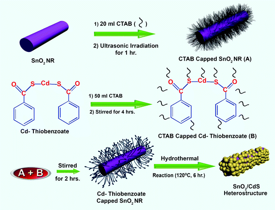
To prepare the SnO2/CdS heterostructure, a hydrothermal method was used. First, 80 ml solution of aqueous CTAB was prepared by dissolving 0.292 g (10 mmol) of CTAB powder in 80 ml of deionised water. Approximately 0.050 g of SnO2 nanorods prepared above were added into 20 ml aqueous CTAB solution and dispersed for 1 h by ultrasonic irradiation. 0.600 g of cadmium thiobenzoate complex was added to the 50 ml aqueous CTAB solution gradually and stirred for 4 h to dissolve. After sonication, the dispersed SnO2 nanorods were added dropwise to the cadmium thiobenzoate solution. The resulting mixture was again stirred for 2 h. The cloudy suspension was placed in a Teflon lined steel chamber which was put into the oven and heated at 120 °C for 6 h. After the reaction was complete, the steel chamber was air-cooled to room temperature. The products were then collected by centrifugation, washed with distilled water and ethanol several times to remove the impurities and finally vacuum dried for 6 h to obtain the heterostructure. The product was faded yellow in color suggesting the deposition of CdS nanoparticles over the SnO2 nanorods. The light yellow powder was collected for characterization. The synthetic procedure for the preparation of the heterostructure is described in Scheme 1.
 |
| | Scheme 1 A scheme for the preparation of the SnO2/CdS heterostructure. | |
2.5. Characterization
The crystalline phases of the prepared powders were identified by X-ray diffraction (XRD) using a Philips model PW-1730 powder X-ray diffractometer using a Cu-Kα source (1.5418 Å radiation). The lattice strain was calculated using the Williamson and Hall method.39| | | βcosθ/λ = 1/D + ηsinθ/λ | (1) |
Where β is the full width at half-maximum (fwhm), θ is the diffraction angle, λ is the X-ray wavelength, D is the effective particle size and η is the effective strain. The strain is calculated from the slope of a plot of βcosθ/λ against sinθ/λ. Transmission Electron Microscopy (TEM, JEOL Model JEM-2100F) was used to understand the core–shell heterostructure. Elemental mapping and line scan EDS measurements of our sample were done with a HAADF-EDS nanoprobe analyzer using a 1.0 nm probe size.
The UV–vis spectra were taken in a UV-2401 PC SHIMADZU spectrophotometer. The optical absorption coefficient α of a semiconductor close to the band edge can be expressed by eqn (2).40
Where
k is a constant,
Eg is the band gap, and
n is a value that depends on the nature of the transition. In this case,
n is equal to ½ for this direct allowed transition. The band gap can be estimated from a plot of (
αhυ)
2versus photon energy. The
emission spectra of the prepared samples were measured using a
fluoro Max-P (Horiba Jobin Yvon) luminescence
spectrometer. For lifetime measurements of our sample, the time correlated single photon counting (
TCSPC) setup is used. The respective emission wavelength is used and the samples are excited at 375 nm using a picosecond diode (IBH Nanoled-375, repetition rate 1.0 MHz). Fourier-transform infrared (
FTIR)
spectroscopy measurements were performed on a SHIMADZU made FTIR-8300
spectrometer using KBr pellets. Thermogravimetric and
differential thermal analysis (
TG and
DTA) curves were obtained from SDT (Quantachrome) with the heating rate of 5 °C per minute from room temperature to 700 °C under a N
2 gas environment. I–V characteristics of the prepared devices, kept in a shielded vacuum chamber, were recorded with a Keithley 6517B electrometer.
The photocatalytic activities of prepared samples were evaluated by the degradation of Congo red dye. Congo red is water soluble, yielding a red colloidal solution with a high absorption band in the UV spectrum located around 498 nm. The chemical structure of Congo red dye is given in Scheme 2. The photocatalysis experiments were carried out in a 50 ml beaker containing about 25 ml of aqueous Congo red solution (0.034 mM). Approximately 2 mg of pure SnO2 nanorods and SnO2/CdS heterostructure was used separately as photocatalyst. The irradiation was done with a 230V UV lamp (UVITEC). The experimental conditions were set up for continuous magnetic stirring and illumination with a 230V UV lamp. The photocatalytic reaction lasted for 4 h. Samples (3 ml) for analysis were extracted with a syringe at each time interval and filtered immediately. Absorbance of the suspension and the initial solution were determined respectively. A UV-2401 PC SHIMADZU spectrophotometer was used at the maximum absorption wavelength of Congo red (λmax = 498 nm). The degradation rate D was calculated according to eqn (3).
Where
A0 shows initial absorbance and
A shows the sample absorbance.
3. Results and discussion
3.1. Structural characterization
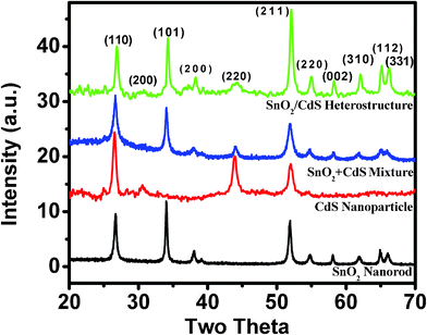
Fig. 1 depicts the XRD patterns of the pure SnO2 nanorods, pure CdS nanoparticles, a physical mixture of CdS and SnO2 nanocrystals and the SnO2/CdS heterostructure prepared under hydrothermal conditions. The X-ray reflections of the uncoated SnO2 nanorods agree with the tetragonal phase of SnO2 (JCPDS card no. 41-1445). No other impurities are detected by XRD analysis, indicating the phase purity of the SnO2 nanorods. X-ray reflections of the CdS nanoparticles match with the cubic phase of CdS (JCPDS card no. 42-1411). The XRD patterns of the physical mixture of CdS and SnO2 and the as-prepared SnO2/CdS heterostructure both show peaks at 30.74° (200), 44.24° (220) and 71.62° (331) which clearly indicates the existence of the cubic phase of CdS (JCPDS card no. 42-1411), along with the tetragonal phase of SnO2. The measured lattice parameter is a = 5.816 Å and the unit cell volume is 0.197 nm3. The cell parameters of the uncoated SnO2 nanorods are a = 4.735 Å, c = 3.175 Å and cell vol. = 0.07119 nm3 which were modified to a = 4.717 Å, c = 3.164 Å and cell vol. = 0.0704 nm3 after surface coating with CdS. This reveals that the heterostructure plays an important role in tuning the cell parameters which may influence the physical properties.
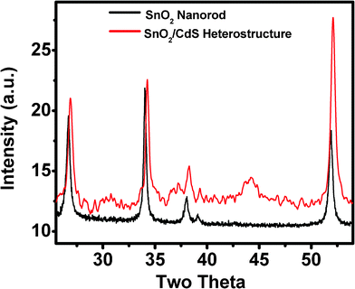
The formation of the CdS shell on SnO2 nanorods is further supported by XRD analysis. Fig. 2 shows the representative XRD patterns of pure SnO2 nanorods and the as-prepared SnO2/CdS heterostructure. The XRD pattern of the SnO2 nanorods consists of the characteristic tetragonal phase with diffractive peaks at 26.71°, 34.05°, 37.97° and 51.86°. It is interesting to note that the diffraction peaks shift to larger angles at 26.89°, 34.26°, 38.24° and 52.11° for the heterostructure, which further confirms the formation of the core–shell heterostructure. The diffraction peaks shift to larger angles in the heterostructure due to the smaller lattice constant for SnO2/CdS nanorods compared with pure SnO2 nanorods. Zhong et al.41 observed the shift of diffraction peaks to larger angles located between the cubic CdTe and CdS phase in CdTe/CdS core–shell nanocrystals. Similar changes in the diffraction pattern were also reported for previous core–shell nanostructures.42–45 We also calculated the lattice strain by plotting βcosθ/λ against sinθ/λ for pure SnO2 nanorods and the SnO2/CdS heterostructure using eqn (1) (ESI, Fig. S3†) and it was found that the slope value is +0.33% for SnO2 nanorods. The positive slope value indicates the tensile strain. However, a negative slope (–0.22%) is observed for the SnO2/CdS heterostructure, indicating the presence of compressive strain. Thus, the lattice strain of core material can be modified by the formation of a shell, in line with previous results.46,47
 |
| | Fig. 2 X-ray powder diffraction patterns of pure SnO2 nanorods and the SnO2/CdS heterostructure, indicating the shifting in peak positions due to core–shell type heterostructure formation. | |
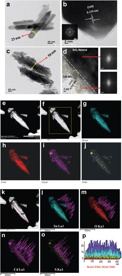
Fig. 3a–d show transmission electron microscopy (TEM) and high resolution transmission electron microscopy (HRTEM) images of the SnO2 nanorods and the SnO2/CdS heterostructure. The TEM image (Fig. 3a) confirms the formation of nearly uniform size and shape SnO2 nanorods. It can be seen from Fig. 3a that SnO2 nanorods have typically smooth surfaces throughout the entire length of the rod with average diameter approximately 20–25 nm and length 120–140 nm. The distance between lattice planes (0.335 nm) corresponds to the (110) plane of the tetragonal phase of SnO2 which is further confirmed by the HRTEM image of a single SnO2 nanorod (Fig. 3b). The SAED pattern of an uncoated SnO2 nanorod (inset of Fig. 3b) confirms the tetragonal phase of SnO2. Fig. 3c clearly shows the complete deposition of CdS nanoparticles on SnO2 nanorods and formation of the heterostructure. The diameter of the nanorods increases to 50 nm from 20–25 nm after deposition of CdS. Fig. 3d shows an HRTEM image of a deposited CdS nanoparticle. The calculated distance between the lattice planes is 0.341 nm which is well matched to the reported value for the (111) plane of the cubic CdS. The SAED patterns of the SnO2/CdS heterostructure were taken from two different positions (Fig. 3d). The same diffraction rings as for cubic structured CdS clearly indicate that the surfaces of the SnO2 nanorods are fully covered by cubic phase CdS nanoparticles. Thus, TEM and HRTEM analysis confirm that the SnO2 nanorods are fully covered by CdS nanoparticles to form SnO2/CdS heterostructures. An elemental mapping and line scan EDS study were done using STEM-HAADF and OXFORD EDS analyzers to further investigate the formation of the heterostructure, shown in Fig. 3e–p. Fig. 3e shows an STEM-HAADF image of a single SnO2/CdS nanorod and the selected area of the STEM-HAADF image for the elemental mapping analysis (Fig. 3f). The elemental mappings are shown in Fig. 3g to 3j. The figures clearly show the well-defined spatial distribution of all the elements present viz. Sn, O, Cd and S. Fig. 3k to 3p represent the TEM-EDS concentration line profiles of Sn, O, Cd and S, measured along the line across the length in the SnO2/CdS nanorod. It is clearly seen that Cd and S are localized throughout the entire nanorod. Analysis confirms the formation of the SnO2/CdS heterostructure.
 |
| | Fig. 3 Transmission electron microscopy (TEM) and HRTEM images of SnO2 nanorods (a and b) and the SnO2/CdS heterostructure (c and d). The insets of (b) and (d) show the SAED patterns of the SnO2 nanorods and SnO2/CdS heterostructure. e and f are STEM-HAADF images of a single SnO2/CdS heterostructure nanorod. EDS elemental mapping of the spatial distribution of Sn (g), O (h), Cd(i) and S (j) elements. k shows an STEM-HAADF image of a single SnO2/CdS heterostructure nanorod and EDS line scans across a single SnO2/CdS nanorod (l–o) for Sn, O, Cd and S elements. TEM-EDS concentration line profile of Sn, O, Cd and S, measured along the line across the length (p). | |
3.2. Optical properties
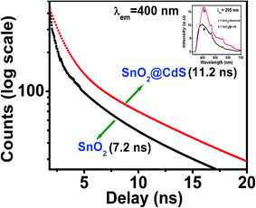
The UV-vis spectra of SnO2 nanorods, CdS nanoparticles and SnO2/CdS heterostructures were measured (ESI, Fig. S4†). Fig. 4 depicts the time resolved photoluminescence (PL) decay curves for SnO2 nanorods and SnO2/CdS heterostructures at their emission wavelength peak (400 nm). The inset plot of Fig. 4 shows the room temperature PL spectrum of the corresponding samples under excitation at 295 nm. The PL spectra of the SnO2 nanorods and the SnO2/CdS heterostructures are broad and asymmetric with the emission peaks centered at approximately 400 nm. The PL intensity of the SnO2/CdS heterostructure was found to be higher than that of uncoated SnO2 nanorods, excited at 295 nm wavelength by a nanoLED-295 laser. The decay curves are fitted with tri-exponentials to obtain the average decay time. The three components of the decay curve are 0.35 ns (64%), 2.19 ns (25%) and 10.83 ns (11%) for the SnO2 nanorods and the average decay time value is 7.2 ns. For the SnO2/CdS heterostructure, the three components are 0.33 ns (82%), 3.14 ns (13%) and 18.05 ns (5%) and the average decay time value is 11.2 ns. Type II heterostructure materials are expected to have longer exciton decay times due to the spatial separation of charges.3 The decrease of effective band gap (3.64 eV to 3.02 eV) and increase of average lifetime value (7.2 ns to 11.2 ns) clearly indicates the effective charge separation in the heterostructure which is consistent with previous results.43
 |
| | Fig. 4 Photoluminescence (PL) decays of SnO2 nanorods and SnO2/CdS heterostructures at 400 nm emission wavelength (inset plot is the corresponding PL spectraum at 295 nm). | |
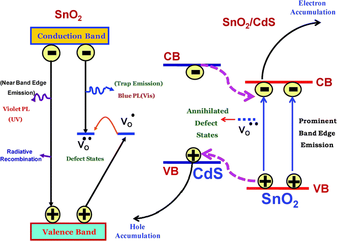
For a detailed understanding of the time resolved photoluminescence (PL) decay curves of the heterostructure, we proposed a schematic model (Fig. 5) to get more insight about the possible electronic interactions between the two semiconductor nanocrystals (SnO2 and CdS). In the left side of the model, we introduce different relaxation processes in the SnO2 nanocrystal. In SnO2, there are three consequent energy levels48viz. valence band (VB), defect states (V·o/V··0) and conduction band (CB). Upon photoexcitation of the SnO2 nanocrystal, it first creates positive holes in the VB and negative electrons in the CB. Two main types of relaxation processes can occur. Firstly, the hole in the VB and electron in the CB can radiatively recombine and secondly, the hole in the VB can trap at the oxygen vacancy sites. Then, this surface trapped hole tunnels back into the nanorod to recombine with an electron in a deep trap V·o centre to form the V··0 centre at the surface of the particle. Then recombination of a V··0 centre with an electron in the CB gives rise to defect emission. In the case of the SnO2/CdS heterostructure, the mechanism is different (right side of the model). Here, SnO2 is a direct wide band gap semiconductor (Eg = 3.61 eV at 300 K) while CdS is a short band gap semiconductor (Eg = 2.40 eV at 300 K).49 The conduction band of CdS (–0.8 V vs. NHE) is more negative than that of SnO2 (0.0 V vs. NHE). Therefore, upon photoexcitation, the photogenerated electrons of CdS can be transferred to the conduction band of SnO2, while the holes of SnO2 can be transferred to the VB of CdS (Fig. 5). Thus, the electron and hole separation become prominent in this heterostructure. Therefore, in the SnO2/CdS heterostructure, the electrons will accumulate in the CB of SnO2 while holes are in the VB of CdS and this effective charge separation in the heterostructure leads to longer exciton decay time.
 |
| | Fig. 5 Schematic model proposed for different relaxation processes in SnO2 nanorods and SnO2/CdS heterostructure nanorods. | |
3.3. Electrical properties
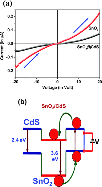
Fig. 6a shows the I–V characteristics for SnO2 nanorods and the SnO2/CdS heterostructure when a voltage is applied between Au and Au terminals in the forward direction. The current vs. voltage characteristics are asymmetric and non-linear (Fig. 6a) for the forward direction of applied voltage for both the samples, indicating the formation of a Schottky barrier in the materials.40 It is known that intrinsic SnO2 is an n-type semiconductor with a work function of 4.5 eV, and that the work function of Au is 5.1 eV. Thus, the Au electrode is made to facilitate electron flow from the SnO2 nanocrystals to the Au electrode since the Fermi level of the SnO2 nanorods is initially higher than that of Au metal before the contact was made.50 This process results in the formation of an electron depleted region at the surface of the SnO2 nanorods that corresponds to a Schottky barrier between the SnO2 nanorods and the Au electrode. Therefore, the Au electrode forms Schottky-barrier contacts with SnO2 nanorods. It is important to mention that the conductivity is found to be lower in the SnO2/CdS heterostructure compared to uncoated SnO2 nanorods. This can be explained as follows: due to type-II interaction between the two semiconductor materials (SnO2 and CdS), efficient charge separation occurs in the heterostructure; electrons are accumulating in the core whereas holes are in the shell (Fig. 6b). Thus, carrier transport is hampered due to the barrier and thus the conductivity decreases. Therefore, this heterostructure acts as a good charge storage material due to efficient charge separation. This charge separation phenomenon is supposed to enhance the photocatalytic activity, which is discussed in a later section.
 |
| | Fig. 6 (a) Current vs. voltage characteristics for SnO2 nanorods and the SnO2/CdS heterostructure when the voltage is applied between Au and Au terminals in a forward bias direction. (b) Schematic representation of the band gap alignment in the type-II SnO2/CdS heterostructure to show the electron–hole separation. | |
3.4. Photocatalytic activity
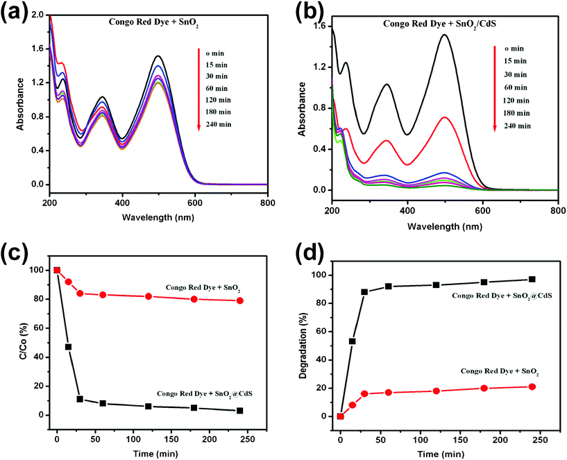
The results of photodecomposition of Congo red dye under UV irradiation (365 nm) are given in Fig. 7. Fig. 7a and b illustrate the relationship between light absorbance and UV irradiation time for pure SnO2 nanorods and the SnO2/CdS heterostructure respectively after 240 min UV irradiation. The Congo red dye showed a major absorption band at 498 nm. It was found that the absorbance band is gradually reduced with increased UV irradiation time in the case of the SnO2/CdS heterostructure whereas for the pure SnO2 nanorods it was almost unchanged. Fig. 7c shows the Congo red decomposition rate as a function of UV irradiation time. Pure SnO2 nanorods and SnO2/CdS heterostructure nanorods were tested for 240 min under identical conditions. C0 and C are the concentrations of Congo red dye before and after UV irradiation respectively. It was found that 97% of the Congo red dye was degraded by the SnO2/CdS heterostructure after 240 min UV irradiation, whereas only 20% degradation was found in the presence of pure SnO2 nanorods. In the absence of both pure SnO2 nanorods and SnO2/CdS heterostructures, decomposition of Congo red dye under the same UV irradiation conditions was negligible. Again, the percentage degradation was calculated using eqn (3) and it was plotted against UV irradiation time in Fig. 7d. The degradations were found to be 97% and 20% for the SnO2/CdS heterostructure and pure SnO2 nanorods respectively. These results clearly demonstrate that the SnO2/CdS heterostructure has significantly improved photocatalytic activity in comparison with pure SnO2 nanorods. The efficient charge separation in the SnO2/CdS heterostructure reveals its higher photocatalytic activity, which is consistent with previous reports.51,52 The SnO2/CdS heterostructure improves the separation of photogenerated electron–hole pairs due to the potential energy differences between SnO2 and CdS, thus enhancing the photocatalytic activity.
 |
| | Fig. 7 (a) and (b) are the absorbance spectral changes of Congo red solution in the presence of pure SnO2 nanorods and the SnO2/CdS heterostructure respectively. (c) Photodegradation rate of Congo red by different photocatalysts (SnO2 and SnO2/CdS) under UV light irradiation for 4 h. (d) The plot of percentage degradation of Congo red vs. UV irradiation time in the presence of pure SnO2 nanorods and the SnO2/CdS heterostructure. | |
4. Conclusion
In conclusion, we have successfully synthesized a SnO2/CdS heterostructure using a hydrothermal method from a single source precursor. XRD, HRTEM, elemental mapping and line scan EDAX analysis confirm the formation of the heterostructure. Time resolved analysis demonstrated the efficient charge separation in the heterostructure. We also proposed a model to explain different relaxation processes in SnO2 and SnO2/CdS heterostructure upon photoexcitation which helps us to understand the type-II type interaction between two semiconductor nanocrystals (SnO2 and CdS). A study of the electrical properties also suggests the occurrence of electron accumulation in the core and hole accumulation in the shell. The photocatalytic activity is enhanced in the SnO2/CdS heterostructure compared to pure SnO2 and this enhancement is due to the efficient charge separation in the heterostructure.
Acknowledgements
We give special thanks to Mr. Supriya Chakraborty, TEM Division, IACS for TEM, elemental mapping and line scan EDS analysis of our samples. CSIR is gratefully acknowledged for financial support. AK and SK also thank CSIR for awarding fellowships.
References
- A. M. Smith and S. Nie, Acc. Chem. Res., 2009, 43, 190–200.
- O. Schöps, N. Le Thomas, U. Woggon and M. V. Artemyev, J. Phys. Chem. B, 2006, 110, 2074–2079 CrossRef CAS.
- S. Kim, B. Fisher, H.-J. Eisler and M. Bawendi, J. Am. Chem. Soc., 2003, 125, 11466–11467 CrossRef CAS.
- M. A. Malik, P. O'Brien and N. Revaprasadu, Chem. Mater., 2002, 14, 2004–2010 CrossRef CAS.
- T. Gao, Q. Li and T. Wang, Chem. Mater., 2005, 17, 887–892 CrossRef CAS.
- K. Palaniappan, C. Xue, G. Arumugam, S. A. Hackney and J. Liu, Chem. Mater., 2006, 18, 1275–1280 CrossRef CAS.
- F. Caruso, Adv. Mater., 2001, 13, 11–22 CrossRef CAS.
- S. K. Panda, A. Dev and S. Chaudhuri, J. Phys. Chem. C, 2007, 111, 5039–5043 CrossRef CAS.
- R. A. Caruso and M. Antonietti, Chem. Mater., 2001, 13, 3272–3282 CrossRef CAS.
- J. Cao, J.-Z. Sun, H.-Y. Li, J. Hong and M. Wang, J. Mater. Chem., 2004, 14, 1203–1206 RSC.
- T. Gao and T. Wang, Chem. Commun., 2004, 2558–2559 RSC.
- S. Yan, D. Hu, F. Hu, J. Wu, N. Huang and Z. Xiao, CrystEngComm, 2011, 13, 4580–4585 RSC.
- C. Nasr, S. Hotchandani, W. Y. Kim, R. H. Schmehl and P. V. Kamat, J. Phys. Chem. B, 1997, 101, 7480–7487 CrossRef CAS.
- R. Kennedy, I. Martini, G. Hartland and P. Kamat, J. Chem. Sci., 1997, 109, 497–507 Search PubMed.
- H. Sun, S.-Z. Kang and J. Mu, J. Dispersion Sci. Technol., 2009, 30, 384–387 Search PubMed.
- F. Xu, V. Volkov, Y. Zhu, H. Bai, A. Rea, N. V. Valappil, W. Su, X. Gao, I. L. Kuskovsky and H. Matsui, J. Phys. Chem. C, 2009, 113, 19419–19423 CrossRef CAS.
- X. Q. Meng, D. X. Zhao, J. Y. Zhang, D. Z. Shen, Y. M. Lu, X. W. Fan and X. H. Wang, Mater. Lett., 2007, 61, 3535–3538 Search PubMed.
- C.-Y. Chen, C.-T. Cheng, J.-K. Yu, S.-C. Pu, Y.-M. Cheng, P.-T. Chou, Y.-H. Chou and H.-T. Chiu, J. Phys. Chem. B, 2004, 108, 10687–10691 CrossRef CAS.
- D. Dorfs, A. Salant, I. Popov and U. Banin, Small, 2008, 4, 1319–1323 CrossRef.
- M. Kong, Y. Li, X. Chen, T. Tian, P. Fang, F. Zheng and X. Zhao, J. Am. Chem. Soc., 2011, 133, 16414–16417 CrossRef CAS.
- J. L. Yang, S. J. An, W. I. Park, G. C. Yi and W. Choi, Adv. Mater., 2004, 16, 1661–1664 CrossRef CAS.
- S. Wu, H. Cao, S. Yin, X. Liu and X. Zhang, J. Phys. Chem. C, 2009, 113, 17893–17898 CrossRef CAS.
- N. Serpone and A. V. Emeline, J. Phys. Chem. Lett., 2012, 3, 673–677 Search PubMed.
- S. G. Kumar and L. G. Devi, J. Phys. Chem. A, 2011, 115, 13211–13241 CrossRef CAS.
- A. Mclaren, T. V. Solis, G. Li and S. C. Tsang, J. Am. Chem. Soc., 2009, 131, 12540–12541 CrossRef CAS.
- M. R. Hoffmann, S. T. Martin, W. Choi and D. W. Bahnemann, Chem. Rev., 1995, 95, 69–96 CrossRef CAS.
- B. Liu, X. Zhao, N. Zhang, Q. Zhao, X. He and J. Feng, Surf. Sci., 2005, 595, 203–211 CrossRef CAS.
- Z. Liu, D. D. Sun, P. Guo and J. O. Leckie, Nano Lett., 2007, 7, 1081–1085 CrossRef CAS.
- J. Pan, S.-M. Hühne, H. Shen, L. Xiao, P. Born, W. Mader and S. Mathur, J. Phys. Chem. C, 2011, 115, 17265–17269 CrossRef CAS.
- C. Wang, X. Wang, B.-Q. Xu, J. Zhao, B. Mai, P. a. Peng, G. Sheng and J. Fu, J. Photochem. Photobiol., A, 2004, 168, 47–52 CrossRef.
- A. Dodd, A. McKinley, M. Saunders and T. Tsuzuki, Nanotechnology, 2006, 17, 692–698 CrossRef CAS.
- L. Zheng, Y. Zheng, C. Chen, Y. Zhan, X. Lin, Q. Zheng, K. Wei and J. Zhu, Inorg. Chem., 2009, 48, 1819–1825 CrossRef CAS.
- X. Yan, C. Zou, X. Gao and W. Gao, J. Mater. Chem., 2012, 22, 5629–5640 RSC.
- D. Chen, H. Zhang, S. Hu and J. Li, J. Phys. Chem. C, 2008, 112, 117–122 CrossRef CAS.
- M. Agrawal, S. Gupta, A. Pich, N. E. Zafeiropoulos and M. Stamm, Chem. Mater., 2009, 21, 5343–5348 CrossRef CAS.
- J. C. Kim, J. Choi, Y. B. Lee, J. H. Hong, J. I. Lee, J. W. Yang, W. I. Lee and N. H. Hur, Chem. Commun., 2006, 5024–5026 RSC.
- P. Kundu, P. A. Deshpande, G. Madras and N. Ravishankar, J. Mater. Chem., 2011, 21, 4209–4216 RSC.
- Z. Sun, Z. Yang, J. Zhou, M. H. Yeung, W. Ni, H. Wu and J. Wang, Angew. Chem., Int. Ed., 2009, 48, 2881–2885 CrossRef CAS.
- G. K. Williamson and W. H. Hall, Acta Metall., 1953, 1, 22–31 CrossRef CAS.
- A. Kar and A. Patra, J. Phys. Chem. C, 2009, 113, 4375–4380 CrossRef CAS.
- Z. Gu, L. Zou, Z. Fang, W. Zhu and X. Zhong, Nanotechnology, 2008, 19, 135604 CrossRef.
- A. Kar, A. Datta and A. Patra, J. Mater. Chem., 2010, 20, 916–922 RSC.
- X. Peng, M. C. Schlamp, A. V. Kadavanich and A. P. Alivisatos, J. Am. Chem. Soc., 1997, 119, 7019–7029 CrossRef CAS.
- R. Xie, U. Kolb, J. Li, T. Basché and A. Mews, J. Am. Chem. Soc., 2005, 127, 7480–7488 CrossRef CAS.
- D. V. Talapin, A. L. Rogach, A. Kornowski, M. Haase and H. Weller, Nano Lett., 2001, 1, 207–211 CrossRef CAS.
- P. Ghosh, E. d. l. Rosa, J. Oliva, D. Solis, A. Kar and A. Patra, J. Appl. Phys., 2009, 105, 113532 CrossRef.
- P. Ghosh, A. Kar and A. Patra, Nanoscale, 2010, 2, 1196–1202 RSC.
- A. Kar, S. Kundu and A. Patra, J. Phys. Chem. C, 2011, 115, 118–124 CrossRef CAS.
- P. Cervantes, Q. Williams, M. Côté, O. Zakharov and M. L. Cohen, Phys. Rev. B: Condens. Matter, 1996, 54, 17585–17590 Search PubMed.
- M. Chen, X. Xia, Z. Wang, Y. Li, J. Li and C. Gu, Microelectron. Eng., 2008, 85, 1379–1381 Search PubMed.
- K. Vinodgopal, I. Bedja and P. V. Kamat, Chem. Mater., 1996, 8, 2180–2187 CrossRef CAS.
- T. Hirakawa and P. V. Kamat, J. Am. Chem. Soc., 2005, 127, 3928–3934 CrossRef CAS.
Footnote |
| † Electronic supplementary information (ES1) available: Fig. S1 shows the FTIR spectrum of the cadmium thiobenzoate complex. Fig. S2 shows the TGA-DTA curve of the cadmium thiobenzoate complex. Fig. S3 shows the plot of βcosθ/λ against sinθ/λ for pure SnO2 nanorods and the SnO2/CdS heterostructure. Fig. S4 shows the UV–vis spectra of SnO2 nanorods, CdS nanoparticles and SnO2/CdS heterostructure. |
|
| This journal is © The Royal Society of Chemistry 2012 |
Click here to see how this site uses Cookies. View our privacy policy here. ![[thin space (1/6-em)]](https://www.rsc.org/images/entities/char_2009.gif) :
:![[thin space (1/6-em)]](https://www.rsc.org/images/entities/char_2009.gif) 1). This basic mixture was added dropwise to the SnCl4·5H2O solution with continuous stirring. A white cloudy suspension was slowly formed at acidic pH. This white suspension slowly disappears with increasing pH and a clear solution was obtained at pH range 11–12. The clear solution (pH = 12.0) was placed in a Teflon lined steel chamber of 110 ml capacity and the steel chamber was placed inside an oven and heated at 180 °C for 12 h. After the reaction was complete, the steel chamber was air-cooled to room temperature. The products were then collected and washed with distilled water and ethanol several times to remove the impurities. The obtained white powdery product was then dried in an oven overnight at 60 °C to get the final product as a white powder.
1). This basic mixture was added dropwise to the SnCl4·5H2O solution with continuous stirring. A white cloudy suspension was slowly formed at acidic pH. This white suspension slowly disappears with increasing pH and a clear solution was obtained at pH range 11–12. The clear solution (pH = 12.0) was placed in a Teflon lined steel chamber of 110 ml capacity and the steel chamber was placed inside an oven and heated at 180 °C for 12 h. After the reaction was complete, the steel chamber was air-cooled to room temperature. The products were then collected and washed with distilled water and ethanol several times to remove the impurities. The obtained white powdery product was then dried in an oven overnight at 60 °C to get the final product as a white powder.
