DOI:
10.1039/C2RA21083E
(Paper)
RSC Adv., 2012,
2, 9423-9436
Facile fabrication of Bi2O3/Bi–NaTaO3 photocatalysts for hydrogen generation under visible light irradiation
Received
30th May 2012
, Accepted 3rd August 2012
First published on 29th August 2012
Abstract
A new series of Bi2O3/Bi–NaTaO3 photocatalysts were fabricated by a modified solid state reaction method. After an optimal amount of bismuth doping into NaTaO3, the incorporated bismuth forms a separate oxide phase instead of remaining in the originally doped form. The band gaps of the Bi2O3/Bi–NaTaO3 samples were tuned to effectively absorb visible light and induced visible light photocatalytic activity, with varying bismuth concentration. Photoluminescence studies confirmed that the optimum amount of bismuth, found to be 0.3 Bi2O3/Bi–NaTaO3, effectively suppresses the recombination rate of photogenerated charge carriers. A further increase in bismuth concentration (>0.3 molar ratio) leads to impurity formation and creates defect states which inhibit the photocatalytic activity of the Bi2O3/Bi–NaTaO3. The energy band positions of Bi2O3 and Bi–NaTaO3 were calculated by PEC measurement. The 0.3 Bi2O3/Bi–NaTaO3 photocatalyst exhibited the highest performance in terms of H2 evolution, i.e. 102.5 μmol h−1 under visible light irradiation (λ ≥400 nm) in aqueous methanol solution as the sacrificial reagent. The photocatalytic activities of Bi2O3/Bi–NaTaO3 composites were explained on the basis of the photosensitizing effect of Bi2O3, electron–hole separation and PL intensity.
1. Introduction
Hydrogen energy is expected to become one of the potential candidates to replace fossil fuels in the near future because of its high-energy capacity, recycling potential and environmentally friendly qualities.1 A number of methods have been attempted to produce hydrogen, such as the electrolysis of water and reforming of hydrocarbons, etc. Actually, these methods can only be considered as short-term H2 solutions because they have significant environmental and energy input concerns.2 Among them, photocatalytic decomposition of water is one route that has great potential for the production of H2, directly from abundant and renewable water and natural sunlight. Therefore, the development of highly efficient and visible-light driven photocatalysts is urgently required from an energy saving, economically viable and environmentally friendly viewpoint. Since the report of Fujishima and Honda on water splitting using a TiO2 photocatalyst,3 numerous attempts have been made towards the development of new semiconductor photocatalysts for efficient water splitting. A comprehensive survey of photocatalytic activity, chemical stability and environmental friendliness shows that the most promising photocatalysts might be titanium, niobium or tantalum-based materials.4 Among these materials, tantalates are a group of highly active photocatalysts for water splitting. Most of these active tantalates are perovskite-related oxide compounds, such as K3Ta3Si2O13,5 A′Ta2O6 (A′: Ca, Sr, and Ba),6,7 KLn2Ta5O15,8 Sr2M2O7 (M = Nb, Ta),9,10 KTaO3,11,12 RbNdTa2O713 and so forth.14 In particular, NiO/La![[thin space (1/6-em)]](https://www.rsc.org/images/entities/char_2009.gif) :
:![[thin space (1/6-em)]](https://www.rsc.org/images/entities/char_2009.gif) NaTaO3, with a perovskite structure, has been proven to be one of the most promising photocatalysts for water splitting reactions with a highest quantum efficiency of 56% at λ = 270 nm.15 Sodium tantalate is an important lead-free perovskite-type ferroelectric material.16 Over the last few years, researchers have paid much attention to the use of ferroelectric materials as photocatalysts.17–19 Ferroelectric materials have internal dipolar fields which can drive photogenerated electrons and holes in opposite directions and hence reduce the electron–hole recombination. The minimisation of electron–hole recombination in the materials greatly enhances the photocatalytic efficiency.20 However, pure NaTaO3 becomes active solely under ultraviolet light, which is only a small part (4%) of solar irradiation. But this material might be a good mother structure for design and development of visible light driven photocatalysts. A number of different attempts have been made to modify NaTaO3 in order to make it active in the visible light region, mainly by doping with cations or anions.21,24 To date, NaTaO3 based visible-light-driven photocatalysts are rare. Recently, some reports have been found on the development of visible-light-driven NaTaO3-based photocatalysts such as Na1−xLaxTa1−xCrxO3,21,22 Na1−xLaxTa1−xCoxO3,23 NaTaO3−xNx,24,25 Ir-La-doped NaTaO3etc.26 Therefore, it is of great interest to develop novel visible-light responsive NaTaO3 photocatalysts. Recently, bismuth-doped NaTaO3 nanoparticles prepared by a hydrothermal method have been studied for photocatalytic reactions. Li et al. reported a visible light active solid solution photocatalyst, i.e. NaTa1−xBixO3. Hydrogen evolution over these nanoparticles was reported without any co-catalyst loading under visible light radiation.27 The optical absorption properties of Bi3+-doped NaTaO3 nanoparticles were also studied by Wang et al., where a small change in the absorption edge of NaTaO3 was observed upon Bi doping.28 Kanhere et al. have studied the effects of Bi doping on Na or Ta or both Na and Ta sites and their optical and photocatalytic decomposition of methylene blue.29 However, there have been no reports so far on Bi2O3/Bi–NaTaO3 and their optical properties and photocatalytic activity towards H2 evolution from aqueous methanol solution. Therefore, detailed investigations on the optical properties and photocatalytic production of hydrogen over Bi2O3/Bi–NaTaO3 powders with different concentrations of Bi are necessary.
NaTaO3, with a perovskite structure, has been proven to be one of the most promising photocatalysts for water splitting reactions with a highest quantum efficiency of 56% at λ = 270 nm.15 Sodium tantalate is an important lead-free perovskite-type ferroelectric material.16 Over the last few years, researchers have paid much attention to the use of ferroelectric materials as photocatalysts.17–19 Ferroelectric materials have internal dipolar fields which can drive photogenerated electrons and holes in opposite directions and hence reduce the electron–hole recombination. The minimisation of electron–hole recombination in the materials greatly enhances the photocatalytic efficiency.20 However, pure NaTaO3 becomes active solely under ultraviolet light, which is only a small part (4%) of solar irradiation. But this material might be a good mother structure for design and development of visible light driven photocatalysts. A number of different attempts have been made to modify NaTaO3 in order to make it active in the visible light region, mainly by doping with cations or anions.21,24 To date, NaTaO3 based visible-light-driven photocatalysts are rare. Recently, some reports have been found on the development of visible-light-driven NaTaO3-based photocatalysts such as Na1−xLaxTa1−xCrxO3,21,22 Na1−xLaxTa1−xCoxO3,23 NaTaO3−xNx,24,25 Ir-La-doped NaTaO3etc.26 Therefore, it is of great interest to develop novel visible-light responsive NaTaO3 photocatalysts. Recently, bismuth-doped NaTaO3 nanoparticles prepared by a hydrothermal method have been studied for photocatalytic reactions. Li et al. reported a visible light active solid solution photocatalyst, i.e. NaTa1−xBixO3. Hydrogen evolution over these nanoparticles was reported without any co-catalyst loading under visible light radiation.27 The optical absorption properties of Bi3+-doped NaTaO3 nanoparticles were also studied by Wang et al., where a small change in the absorption edge of NaTaO3 was observed upon Bi doping.28 Kanhere et al. have studied the effects of Bi doping on Na or Ta or both Na and Ta sites and their optical and photocatalytic decomposition of methylene blue.29 However, there have been no reports so far on Bi2O3/Bi–NaTaO3 and their optical properties and photocatalytic activity towards H2 evolution from aqueous methanol solution. Therefore, detailed investigations on the optical properties and photocatalytic production of hydrogen over Bi2O3/Bi–NaTaO3 powders with different concentrations of Bi are necessary.
In this manuscript, we synthesized a series of Bi2O3/Bi–NaTaO3 photocatalysts with varying bismuth concentrations through a modified solid state reaction method. The impact of bismuth concentration on the crystal structure, morphology, optical properties, photoelectrochemical properties and photocatalytic activity towards hydrogen production over aqueous methanol solution were discussed in detail.
2. Experimental
2.1. Synthesis of Bi2O3/Bi–NaTaO3
The NaTaO3, Bi–NaTaO3 and Bi2O3/Bi–NaTaO3 photocatalysts were prepared by a modified solid state reaction method using sodium oxalate Na2C2O4 (BDH AR, purity 99.99%), tantalum oxide Ta2O5 (Fluka AG, purity >99.99%) and bismuth nitrate Bi(NO3)3·5H2O (Merck AR, purity 99.9%). The chemicals were mixed with the molar ratio [Na]![[thin space (1/6-em)]](https://www.rsc.org/images/entities/char_2009.gif) :
:![[thin space (1/6-em)]](https://www.rsc.org/images/entities/char_2009.gif) [Bi]
[Bi]![[thin space (1/6-em)]](https://www.rsc.org/images/entities/char_2009.gif) :
:![[thin space (1/6-em)]](https://www.rsc.org/images/entities/char_2009.gif) [Ta] = 1 − x
[Ta] = 1 − x![[thin space (1/6-em)]](https://www.rsc.org/images/entities/char_2009.gif) :
:![[thin space (1/6-em)]](https://www.rsc.org/images/entities/char_2009.gif) x
x![[thin space (1/6-em)]](https://www.rsc.org/images/entities/char_2009.gif) :
:![[thin space (1/6-em)]](https://www.rsc.org/images/entities/char_2009.gif) 1 (where x = 0–0.5) followed by the addition of urea (SDS AR, purity 99.5%) powder. In the present study, the molar ratio of urea to metal ions was kept at [urea]
1 (where x = 0–0.5) followed by the addition of urea (SDS AR, purity 99.5%) powder. In the present study, the molar ratio of urea to metal ions was kept at [urea]![[thin space (1/6-em)]](https://www.rsc.org/images/entities/char_2009.gif) :
:![[thin space (1/6-em)]](https://www.rsc.org/images/entities/char_2009.gif) [Na2C2O4 + Bi (NO3)3·5H2O + Ta2O5] = 2
[Na2C2O4 + Bi (NO3)3·5H2O + Ta2O5] = 2![[thin space (1/6-em)]](https://www.rsc.org/images/entities/char_2009.gif) :
:![[thin space (1/6-em)]](https://www.rsc.org/images/entities/char_2009.gif) 1. The mixtures (Ta2O5, Na2C2O4, Bi(NO3)3·5H2O and urea) were ground thoroughly in a mortar and transferred into a crucible. Then the mixture was activated in a muffle furnace with the heating rate of 2 °C min−1 ranging from room temperature to 300 °C, 5 °C min−1 ranging from 300 to 600 °C and kept at 600 °C for 4 h. For simplicity, Bi doped NaTaO3 prepared at a Bi concentration of 0.05 molar ratio is designated as Bi–NaTaO3 and Bi2O3/Bi–NaTaO3 photocatalysts prepared by varying the bismuth concentration from 0.1–0.5 molar ratio are designated as 0.1 Bi2O3/Bi–NaTaO3, 0.2 Bi2O3/Bi–NaTaO3, 0.3 Bi2O3/Bi–NaTaO3, 0.4 Bi2O3/Bi–NaTaO3, 0.5 Bi2O3/Bi–NaTaO3 respectively. The Bi2O3 was also prepared by same method.
1. The mixtures (Ta2O5, Na2C2O4, Bi(NO3)3·5H2O and urea) were ground thoroughly in a mortar and transferred into a crucible. Then the mixture was activated in a muffle furnace with the heating rate of 2 °C min−1 ranging from room temperature to 300 °C, 5 °C min−1 ranging from 300 to 600 °C and kept at 600 °C for 4 h. For simplicity, Bi doped NaTaO3 prepared at a Bi concentration of 0.05 molar ratio is designated as Bi–NaTaO3 and Bi2O3/Bi–NaTaO3 photocatalysts prepared by varying the bismuth concentration from 0.1–0.5 molar ratio are designated as 0.1 Bi2O3/Bi–NaTaO3, 0.2 Bi2O3/Bi–NaTaO3, 0.3 Bi2O3/Bi–NaTaO3, 0.4 Bi2O3/Bi–NaTaO3, 0.5 Bi2O3/Bi–NaTaO3 respectively. The Bi2O3 was also prepared by same method.
In this method, urea plays two important roles: complexing agent and fuel. During the reaction process, firstly the urea begins melting into a liquid (melting point: 135 °C) with rising temperature. The molten urea then provides a liquid medium in which the diffusion coefficient is higher than that in the solid medium. In the liquid environment Ta2O5, Na2C2O4 and Bi(NO3)3 react easily with urea to form the Ta–urea complex, Na–urea complex and Bi–urea complex. Meanwhile, the ignition of urea generates a large amount of heat and results in an instantaneous high local temperature around 1500 °C (inside the reactants), which ignites the metal-precursors at a temperature much lower than the actual phase formation temperature.16 This temperature will be sufficient to form the crystallized Bi2O3/Bi–NaTaO3 powder. Therefore, the molten urea and combustion of urea play an important role in the whole process.
2.2. Methods of characterization
The samples were characterized by powder X-ray diffraction (PXRD) patterns, BET-surface area, diffuse reflectance UV-vis (DRUV-vis), field emission scanning electron microscopy (FESEM), transmission electron microscopy (TEM), high resolution image transmission electron microscopy (HRTEM), energy dispersive X-ray spectroscopy (EDAX), photoluminescence spectroscopy (PL spectra), X-ray photoelectron spectroscopy (XPS) and photoelectrochemical measurements. The powder X-ray diffraction pattern was recorded on RINT-UltimaIII, Rigaku diffractometer with automatic control. The patterns were run with monochromatic Cu-Kα radiation from 2θ = 10–80° with a scan rate of 2° min−1. Field emission scanning electron microscopy (FESEM) images were taken on a Zeiss Supra 55. Transmission electron microscopy (TEM) and high resolution transmission electron microscopy (HRTEM) were obtained on a Philips TECHNAI G2 operated at 200 kV, in which samples were prepared by dispersing the powdered samples in 2-propanol by sonication for 3 min and then drop-drying on a copper grid coated with carbon film. Optical absorbance was measured by diffuse reflectance UV-vis (DRUV-vis) spectra of the catalyst samples with a Varian Cary 100 spectrophotometer equipped with a diffuse reflectance accessory in the region 200–800 nm, with boric acid as the reference. Photoluminescence spectra were recorded with a Jasco FP-6600 spectrofluorimeter. The PL spectra were measured at liquid nitrogen temperature under excitation at 300 nm, provided by emission from a xenon lamp. The Bi content in the sample before and after the preparation of the photocatalysts was analysed by atomic absorption spectroscopy (AAS, Shimadzu AA-6300) and X-ray photoelectron spectroscopy (XPS; ESCA-3200, Shimadzu) by using Al-Kα X-ray source. The binding energy correction was performed using the C1s peak of carbon at 285 eV as a reference. For photoelectrochemical measurements, the electrodes were prepared by electrophoretic deposition in an acetone solution (50 mL) containing photocatalyst powder (40 mg) and iodine (10 mg). Two parallel FTO electrodes were immersed in the solution with a 10–15 mm separation, and a 50 V bias was applied between the two for 3 min under potentiostat control. The coated area was fixed at 1 cm × 3 cm and then dried. The photoelectrochemical measurement was performed using a conventional Pyrex electrochemical cell consisting of a prepared electrode, a platinum wire as a counter electrode (1 mm in diameter, 15 mm in length) and an Ag/AgCl reference electrode. The cell was filled with an aqueous solution of 0.1 M Na2SO4 and the pH of the solution was adjusted to 6.5. The electrolyte was saturated with argon prior to electrochemical measurements and the potential of the electrode was controlled by a potentiostat (HZ-5000, Hokuto Denko; SDPS-501C, Syrinx). Irradiation was performed through the conducting glass using a 300 W Xe lamp with a cold mirror and cut-off filters (Hoya) as necessary. The current vs. potential (I–V) measurement was done by using a potentiostat (Versastat 3, Princeton Applied Research) with 300 W Xe lamp. This measurement follows the same process as that of the photoresponse experiment. It should be noted that the FTO (fluorine doped tin oxide) did not show a photoresponse in the solution.
2.3. Photocatalytic hydrogen evolution using aqueous methanol solution
The catalytic activity and deactivation were studied in a batch reactor. About 0.1 g of catalyst was suspended in 100 ml of an aqueous solution containing 10 vol.% of CH3OH solution for H2 evolution. The solution was kept under stirring with a magnetic stirrer, prohibiting particles to settle at the bottom of the reactor. Prior to irradiation, the reaction mixture was purged with N2 in order to remove dissolved gases. A 125 W medium pressure Hg lamp was used as the visible light source and 1 M NaNO2 solution is used as a UV filter. The evolved gas was collected by the water displacement technique and analyzed by GC-17A using a 5 Å molecular sieve column with a thermal conductivity detector (TCD). A comparison of the retention time of the peak that appeared on the chromatogram with standards confirmed that the evolved gas was hydrogen.
3. Results and discussion
3.1. Structural characterization
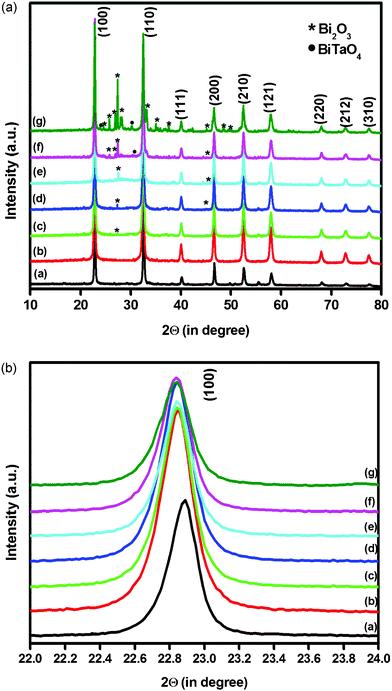
The PXRD patterns of neat NaTaO3, Bi–NaTaO3 and Bi2O3/Bi–NaTaO3 photocatalysts are shown in Fig. 1(a). In all the samples, the prominent diffraction peaks relate to the monoclinic phase of NaTaO3 according to JCPDS card FileNo. 74-2478. The lower concentration of Bi (0.05 molar ratio) does not affect the crystal structure of the NaTaO3. In addition, no significant diffraction peak of Bi species was observed due to the higher dispersion of Bi over the NaTaO3 cube. The main diffraction peak of NaTaO3 shifted slightly towards the lower angle region at lower bismuth concentrations (0.05 molar ratio) and no further shift was observed when the Bi concentration increased from 0.1–0.5 molar ratio, as shown in Fig. 1(b). The shift indicated that lower amounts of bismuth were homogeneously doped into the NaTaO3 lattice, because the ionic radii of Bi3+ (1.34 Å) and Na+ (1.39 Å) ions are very similar. If Bi3+ ions are replaced with Ta5+ ions in NaTaO3 structures, a large shift should be observed due to the large difference in ionic radius of Bi3+ (1.34 Å) and Ta5+ (0.64 Å) ions. Moreover, the diffraction pattern of Bi doped NaTaO3, with the perovskite structure similar to NaTaO3, was observed at a lower angle than that of NaTaO3. Therefore, the small shifts to lower angles observed in the diffraction patterns of Bi doped NaTaO3 suggested the substitution of bismuth ions for sodium ions which occupied A sites in perovskite structures.30 Besides the main diffraction of NaTaO3, the additional diffraction peaks of Bi2O3 with monoclinic phase (JCPDS card File No. 41-1449) were also indexed in Fig. 1(a). The diffraction peaks of Bi2O3 started to appear and intensified gradually with increasing bismuth concentration from a 0.1–0.5 molar ratio. The Bi2O3 related peaks in the XRD spectra indicate that beyond a certain Bi concentration (0.05 molar ratio), the incorporated bismuth forms a separated oxide phase in addition to doping. Thus, we can confirm that the fabricated Bi2O3/Bi–NaTaO3 samples with varying Bi concentration from 0.1–0.5 molar ratio have a mixture of two-phase composition: i.e. monoclinic phase of both Bi–NaTaO3 and Bi2O3. The intensity of the XRD peaks increased with lower bismuth concentration (0.05 molar ratio) but decreased gradually upon increasing the Bi concentration from a 0.1–0.5 molar ratio. The initial increase of NaTaO3 peak intensity was due to the incorporation of Bi into the NaTaO3 lattice. However a higher bismuth concentration causes the samples to be poorly crystalline due to formation of Bi2O3 as a separate phase.24 Moreover, impurities such as BiTaO4 were found when the Bi content was greater than 0.3 molar ratio. Pure NaTaO3 and Bi–NaTaO3 have a surface area of 2.02 m2 g−1 and 2.16 m2 g−1 whereas the surface area of 0.1 Bi2O3/Bi–NaTaO3, 0.2 Bi2O3/Bi–NaTaO3, 0.3 Bi2O3/Bi–NaTaO3, 0.4 Bi2O3/Bi–NaTaO3, 0.5 Bi2O3/Bi–NaTaO3 are found to be 2.26, 2.36, 2.71, 2.82, 2.39 m2 g−1, respectively. When Bi was introduced into NaTaO3, the surface area of the photocatalysts is slightly increased. Since the surface area and particle size are inversely related to each other, the increasing surface area signifies that Bi concentration may inhibit the growth of the particle.31,32
 |
| | Fig. 1 (a) X-ray diffraction patterns of (a) NaTaO3 (b) Bi–NaTaO3 (c) 0.1 Bi2O3/Bi–NaTaO3 (d) 0.2 Bi2O3/Bi–NaTaO3 (e) 0.3 Bi2O3/Bi–NaTaO3 (f) 0.4 Bi2O3/Bi–NaTaO3 (g) 0.5 Bi2O3/Bi–NaTaO3; (b) Enlarged profile of the (100) diffraction pattern of (a) NaTaO3 (b) Bi–NaTaO3 (c) 0.1 Bi2O3/Bi–NaTaO3 (d) 0.2 Bi2O3/Bi–NaTaO3 (e) 0.3 Bi2O3/Bi–NaTaO3 (f) 0.4 Bi2O3/Bi–NaTaO3 (g) 0.5 Bi2O3/Bi–NaTaO3. | |
3.2. Optical properties and band gap
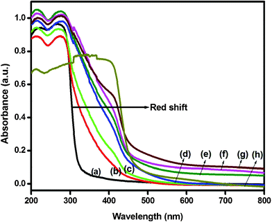
Photoabsorbance of the undoped NaTaO3, Bi–NaTaO3, Bi2O3/Bi–NaTaO3 and pure Bi2O3 photocatalysts were examined by using a diffuse reflectance UV-vis spectrometer. Fig. 2 shows the typical diffuse reflectance spectrum of undoped NaTaO3, pure Bi2O3, Bi–NaTaO3 and Bi2O3/Bi–NaTaO3 photocatalysts at different bismuth concentrations. From the optical absorption spectra, we can see that pure Bi2O3 and all the Bi2O3/Bi–NaTaO3 photocatalysts are harvesting the visible light, while pure NaTaO3 and Bi–NaTaO3 had no absorption in the visible region i.e. it can only harvest UV light due to its large band gap. The absorption edges of pure NaTaO3, Bi–NaTaO3 and Bi2O3 samples are roughly estimated from the absorption onset occurring at 311.5 nm (NaTaO3), 348 nm (Bi–NaTaO3) and 450 nm (Bi2O3) respectively, and accordingly the band gap energies are estimated to be about 3.98, 3.56 and 2.8 eV respectively. However, the Bi2O3/Bi–NaTaO3 photocatalysts showed two different absorption edges at 348 nm and 450 nm respectively. The absorption edges at about 348 nm and 450 nm in the Bi2O3/Bi–NaTaO3 photocatalysts was due to the absorption of Bi–NaTaO3 and Bi2O3 respectively. The absorptions after Bi2O3 formation are drastic and stronger in the visible region. Furthermore, the absorption strengthens with increasing bismuth concentration. This is due to the photosensitization effect of Bi2O3 nanoparticles which could extend the spectral response of Bi–NaTaO3 from the UV to the visible region, making the Bi2O3/Bi–NaTaO3 photocatalysts easily activated by visible light. The remarkable red-shifting of absorption edges of the Bi2O3/Bi–NaTaO3 to longer wavelengths suggest that Bi2O3/Bi–NaTaO3 could be responsive to incident photons of lower energy.33 It is expected that Bi2O3 contributed to the red shift due to narrowing of the band gap of the composite samples, which is evidenced by the colour change of the samples from the original white of NaTaO3 to the slight yellow of Bi–NaTaO3, and pale yellow to deep yellow of Bi2O3/Bi–NaTaO3 samples. The pre-edge absorption became stronger with increasing bismuth concentration and its intensity increased with further increase of bismuth concentration. The fact that the pre-edge absorption became stronger with increasing bismuth concentration may be due to the presence of defect states and formation of Bi2O3 as a separate oxide phase in the materials.34,35
 |
| | Fig. 2 Photoabsorbance spectra of (a) NaTaO3 (b) Bi–NaTaO3 (c) 0.1 Bi2O3/Bi–NaTaO3 (d) 0.2 Bi2O3/Bi–NaTaO3 (e) 0.3 Bi2O3/Bi–NaTaO3 (f) 0.4 Bi2O3/Bi–NaTaO3 (g) 0.5 Bi2O3/Bi–NaTaO3 (h) Bi2O3. | |
3.3. Morphology
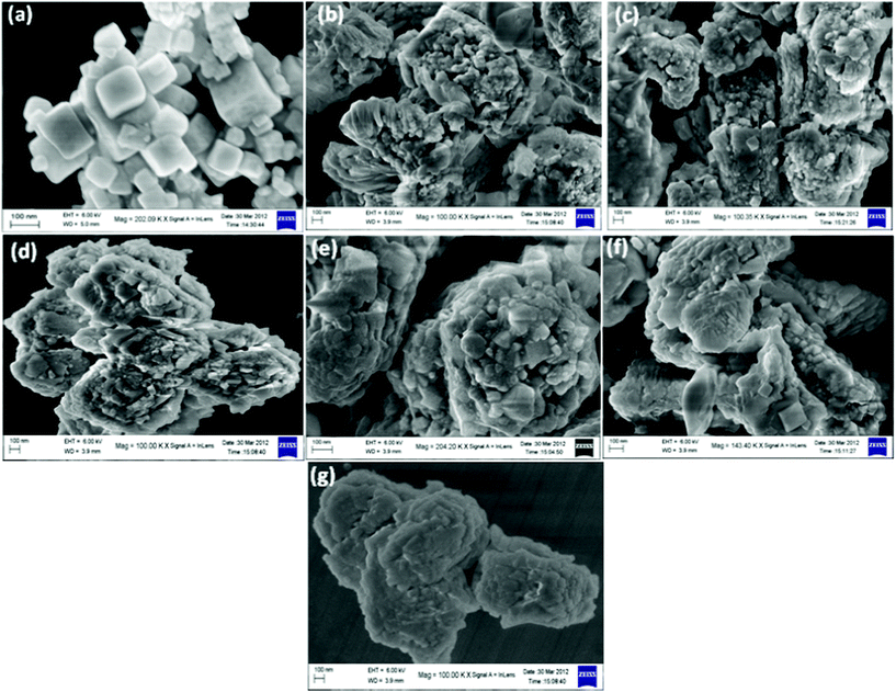
The surface morphology of the photocatalysts NaTaO3, Bi–NaTaO3 and Bi2O3/Bi–NaTaO3 were examined by using field emission scanning electron microscopy (FESEM) as shown in Fig. 3. A cubic morphology was observed in the case of NaTaO3, whereas irregular shaped morphology was found when Bi was doped into NaTaO3. The two samples show different surface morphologies; in contrast to the smooth surface of the NaTaO3 particle, a rough surface was found in the case of Bi–NaTaO3 as shown in Fig. 3(a,b). These results clearly indicate the effect of bismuth concentration on the morphology of NaTaO3. With increasing bismuth concentration, the surface morphologies of the Bi2O3/Bi–NaTaO3 samples changed. When bismuth concentration increased from 0.1–0.5 molar ratio, the agglomeration of Bi2O3 particles formed on the surface of Bi–NaTaO3 as shown in Fig. 3(c–g).
 |
| | Fig. 3 FESEM images of (a) NaTaO3 (b) Bi–NaTaO3 (c) 0.1 Bi2O3/Bi–NaTaO3 (d) 0.2 Bi2O3/Bi–NaTaO3 (e) 0.3 Bi2O3/Bi–NaTaO3 (f) 0.4 Bi2O3/Bi–NaTaO3 (g) 0.5 Bi2O3/Bi–NaTaO3. | |
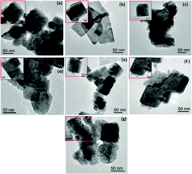
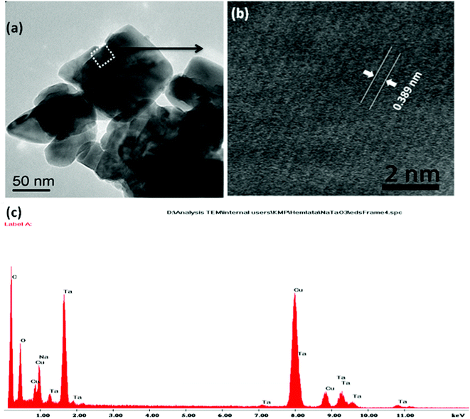
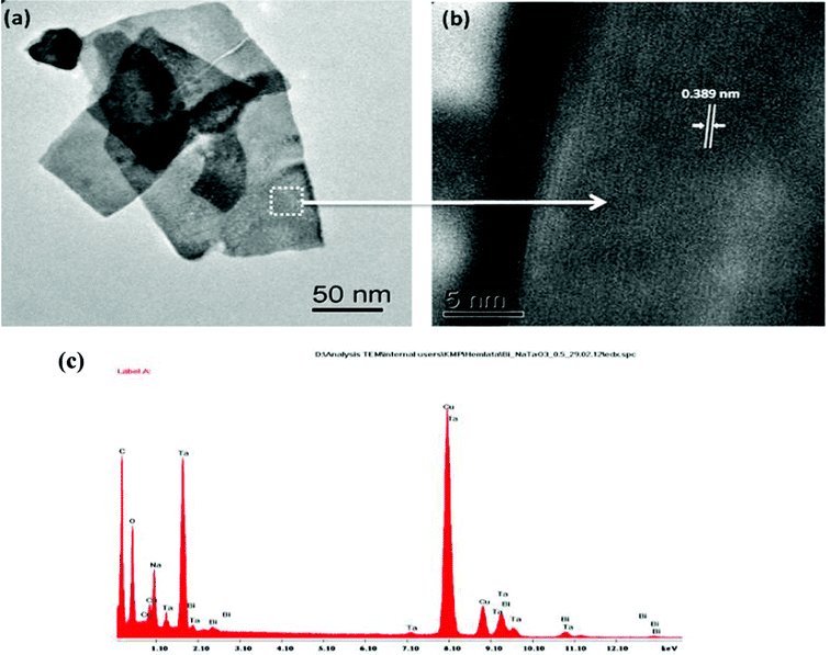
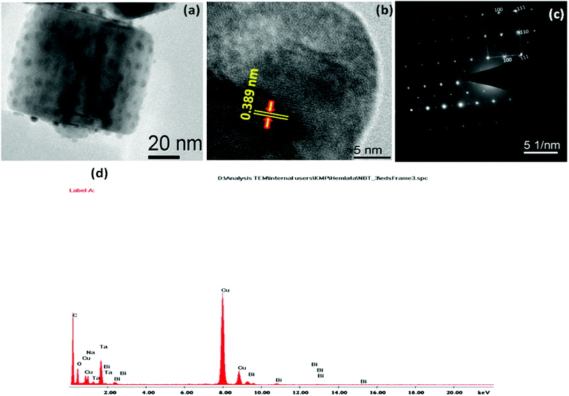
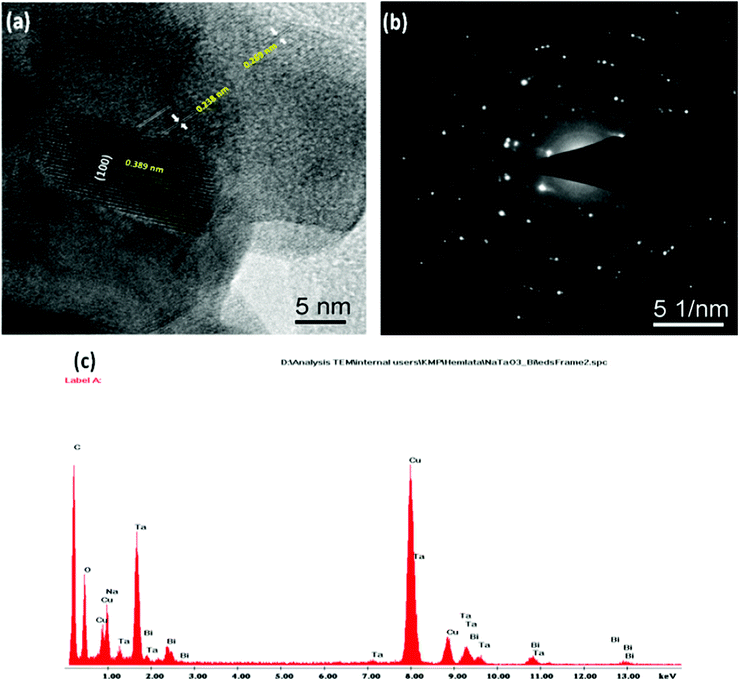
Fig. 4(a–f) shows the TEM micrographs of the undoped NaTaO3, Bi–NaTaO3 and Bi2O3/Bi–NaTaO3 samples, from which one could see that all of the samples exhibit an agglomerated cubic morphology. TEM imaging of the NaTaO3, Bi–NaTaO3 and Bi2O3/Bi–NaTaO3 powder samples revealed cubes with sizes greater than 100 nm. Most of the particles appeared as perfect cubes, as can be seen in the inset of Fig. 4(a–f). Bi incorporation into NaTaO3 results in a rough surface morphology which is consistent with the SEM micrographs. Another observation from the TEM micrographs is that when the concentration of Bi increases in Bi2O3/Bi–NaTaO3, the particle size of Bi2O3 also increases. Fig. 5 and 6 show the HRTEM images of NaTaO3 and Bi–NaTaO3. Fig. 5(b) shows the HRTEM of NaTaO3, a smooth image of the area labelled with a white dotted line in Fig. 5(a). The d-spacing of 0.389 nm corresponds to the (100) plane of NaTaO3 (Fig. 5(b)). The HRTEM image of NaTaO3 with clear lattice fringes confirms the highly crystalline nature of NaTaO3. The EDAX indicates the presence of Na, Ta and O in the NaTaO3 sample (Fig. 5(c)). Fig. 6(b) showed the HRTEM image of Bi–NaTaO3 of the area labelled with a white dotted line in Fig. 6(a). The d-spacing of 0.389 nm corresponds to the (100) plane of Bi–NaTaO3 (Fig. 6(b)). Bi–NaTaO3 showed the same d-spacing as that of NaTaO3, due to the homogenous doping of Bi ions for Na ions in the NaTaO3 structure. The EDAX indicates the presence of Na, Ta, Bi and O in the Bi–NaTaO3 sample (Fig. 6(c)). The HRTEM image of Bi–NaTaO3 with clear lattice fringes confirms the highly crystalline nature of Bi–NaTaO3. The HRTEM image of 0.3 Bi2O3/Bi–NaTaO3 clearly demonstrates the existence of nanoparticles of bismuth oxide distributed over a single cube of Bi–NaTaO3 and the micrograph shows many nanoparticles of Bi2O3 with a size ranging between 3–5 nm, as shown in Fig. 7(a). Fig. 7(b) shows that 0.3 Bi2O3/Bi–NaTaO3 exhibits clearly resolved lattice fringes with the interplanar d-spacing of 0.389 nm assigned to the (100) plane of the monoclinic Bi–NaTaO3 structure, indicating the formation of high-quality 0.3 Bi2O3/Bi–NaTaO3. A spot pattern from a 0.3 Bi2O3/Bi–NaTaO3 single-crystal cube is shown in Fig. 7(c). The bright spots in the diffraction pattern of the 0.3 Bi2O3/Bi–NaTaO3 nanocube are well matched with the (100), (111) and (110) planes of monoclinic Bi–NaTaO3. Fig. 7(d) displays the EDAX spectrum of 0.3 Bi2O3/Bi–NaTaO3 taken in the TEM mode. EDAX indicates the presence of Na, Ta and Bi in the 0.3 Bi2O3/Bi–NaTaO3 sample. The TEM image and electron diffraction pattern of all the 0.3 Bi2O3/Bi–NaTaO3 samples reveals the formation of well-crystallized 0.3 Bi2O3/Bi–NaTaO3. The HRTEM image of 0.5 Bi2O3/Bi–NaTaO3 was shown in Fig. 8(a). Fig. 8(a) shows that the 0.5 Bi2O3/Bi–NaTaO3 composite exhibits clearly resolved lattice fringes with the interplanar d-spacing values of 0.269 and 0.238 nm, indexed to the (122) and (113) planes of monoclinic Bi2O3, while the d value of 0.389 nm is consistent with the (100) plane of Bi–NaTaO3. The HRTEM image and electron diffraction pattern reveals that well-crystallized 0.5 Bi2O3/Bi–NaTaO3 was formed (Fig. 8(a) and (b)). EDAX indicates the presence of Na, Ta and Bi in the 0.5 Bi2O3/Bi–NaTaO3 sample (Fig. 8(c)).
 |
| | Fig. 4 TEM micrographs of (a) NaTaO3 (b) Bi–NaTaO3 (c) 0.1 Bi2O3/Bi–NaTaO3 (d) 0.2 Bi2O3/Bi–NaTaO3 (e) 0.3 Bi2O3/Bi–NaTaO3 (f) 0.4 Bi2O3/Bi–NaTaO3 (g) 0.5 Bi2O3/Bi–NaTaO3. | |
3.4. Photoluminescence (PL) spectra
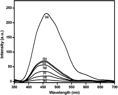
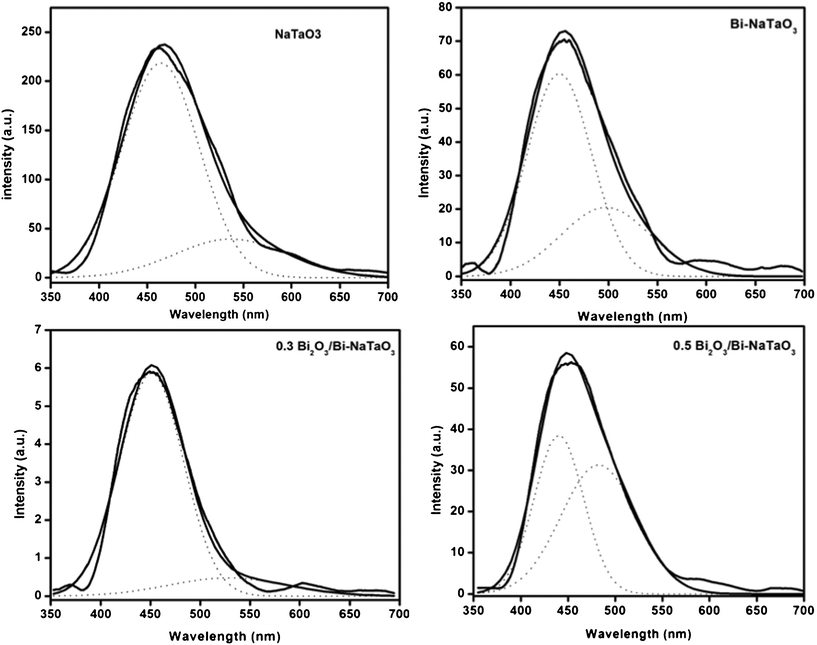
The PL spectra of the semiconductors are useful to disclose the migration, transfer and recombination processes of the photogenerated electron–hole pairs, since PL emission results from the recombination of free charge carriers. The PL spectra of the undoped NaTaO3, Bi–NaTaO3 and Bi2O3/Bi–NaTaO3 photocatalysts under liquid N2 conditions with excitation at 300 nm are presented in Fig. 9. If the number of emitted electrons resulting from the recombination between excited electrons and holes is increased, the PL intensity increases and consequently, the photoactivity decreases.36 For weaker PL intensity, the migration time of photoinduced charge carriers from the inside to the surface is short. Thus, the photoinduced charge carriers have a greater chance to reach the surface in advance of the recombination.37 The emission intensity changes with varying Bi concentration, and increases with decreasing photocatalytic activity of the catalysts (Fig. 9). The PL spectra of all the Bi2O3/Bi–NaTaO3 samples have similar patterns and are located in a similar wavelength region. Therefore, the emission should be intrinsic in origin for NaTaO3 and correspond to a self-trapped exciton.34 To understand the luminescence mechanism, the PL spectra deconvoluted into two peaks that were fitted to a symmetric Gaussian function. Fig. 10 shows the peak resolution results for the luminescence, showing that two Gaussian peaks located at λ > 440 nm and λ > 500 nm constitute the PL spectra of the NaTaO3, Bi–NaTaO3, 0.3 Bi2O3/Bi–NaTaO3 and 0.5 Bi2O3/Bi–NaTaO3 samples. Many researchers have accepted that the origin of visible luminescence in perovskite-type tantalates (ATaO3)38–40 or titanates (ATiO3)41–43 is due to the recombination of trapped electrons and holes (excitons), which is a characteristic feature of PL.44 The luminescence emission in the region 450 nm is called “blue luminescence” (BL), which is attributed due to the intrinsic radiative emission related to the electron–hole pair recombination of a localized exciton in a TaO6 octahedron.41 The lowest BL emission, observed in 0.3 Bi2O3/Bi–NaTaO3, results from improved charge separation; that is why it shows the highest photocatalytic activity towards hydrogen evolution. The emission peaks in the region of 500 nm, called “green luminescence” (GL), can be attributed to an extrinsic defect radiation.34,45,46 This emission could have originated from a large quantity of localized defect states related to vacancies and the formation of an unwanted phase at the grain boundaries, trapping the migrating excitons.45 When Bi concentration exceeds 0.3 molar ratio, the GL intensity of the Bi2O3/Bi–NaTaO3 samples increases, due to the increase in defect states and the formation of other phases such as BiTaO4, which was confirmed from the XRD pattern. The decreased activity of the catalysts with high-level bismuth concentrations is attributed to the defect/impurity formation which is due to the large amount of bismuth incorporated into the NaTaO3.
 |
| | Fig. 9 Photoluminescence emission spectra of (a) NaTaO3 (b) Bi–NaTaO3 (c) 0.1 Bi2O3/Bi–NaTaO3 (d) 0.2 Bi2O3/Bi–NaTaO3 (e) 0.3 Bi2O3/Bi–NaTaO3 (f) 0.4 Bi2O3/Bi–NaTaO3 (g) 0.5 Bi2O3/Bi–NaTaO3 catalysts measured at −196 °C with 300 nm wavelength excitation. | |
 |
| | Fig. 10 The spectra of NaTaO3, Bi–NaTaO3, 0.3 Bi2O3/Bi–NaTaO3, 0.5 Bi2O3/Bi–NaTaO3 were deconvoluted into two Gaussian peaks at ca. λ > 440 and λ > 500 nm. | |
Overall, the charge transport mechanism explained by the PL study along with the structural data from XRD analysis confirmed the role of the Bi species in the distorted perovskite NaTaO3 as well as forming localized defect states or impurities such as BiTaO4 to promote the defect radiation.
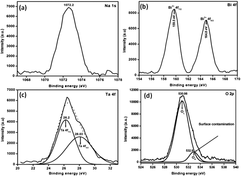
To investigate the formal oxidation state and chemical environment of the 0.3 Bi2O3/Bi–NaTaO3 sample, X-ray photoemission (XPS) spectroscopy analysis was carried out. The narrow-scan XPS spectra of the Na 1s, O 1s, Ta 4f and Bi 4f peaks for the surface of the 0.3 Bi2O3/Bi–NaTaO3 are shown in Fig. 11. The Na 1s peak in the 0.3 Bi2O3/Bi–NaTaO3 was observed at 1072.2 eV and is thus assignable to the Na+ cation (Fig. 11(a)).47 The two strong peaks for the Bi region at 164.8 and 159.5 eV (Fig. 11(b)) are assigned to the Bi 4f5/2 and Bi 4f7/2 peaks of Bi3+ in the short Bi–O bonds.48 The Ta (4f) and O (1s) XPS spectrum was decomposed using 100% Gaussian curve fitting following Shirley background subtraction. The binding energies located at 26.2 and 28.03 eV correspond to Ta (4f7/2) and Ta (4f5/2) respectively for the core levels of Ta5+ cations as shown in Fig. 11(c).49 On the other hand, the two Gaussian peaks are located at 530.98 and 532.9 eV respectively for O (1s) spectrum. The lower binding energy peak corresponds to the O (1s) core level of the O2− anions in 0.3 Bi2O3/Bi–NaTaO3. The O (1s) peak is related to the Ta–O, Na–O and Bi–O chemical bonding.49–52 The higher binding energy peak is attributed to surface contamination, such as carbon oxides or hydroxides.50–53
 |
| | Fig. 11 XPS spectra for 0.3 Bi2O3/Bi–NaTaO3 in the regions of (a) Na-1s, (b) Bi-4f, (c) Ta-4f and (d) O-2p. | |
3.6. Photoelectrochemical (PEC) study
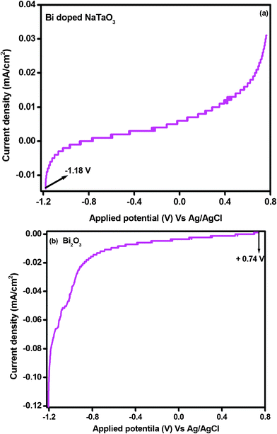
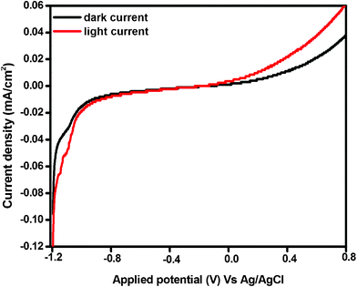
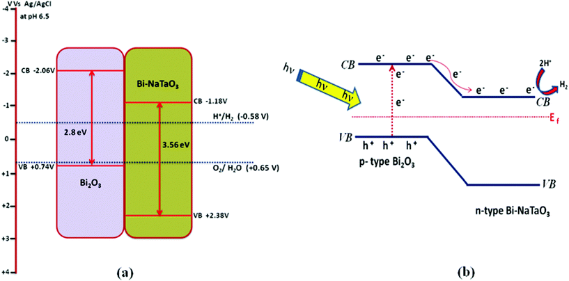
In order to elucidate the relative band edge position of Bi2O3 and Bi–NaTaO3, the photoelectrochemical method has been adopted. Generally, the migration of photoinduced charge carriers depends on their corresponding band edge position. The photocurrent spectra of Bi–NaTaO3 and Bi2O3 are shown in Fig. 12(a) and (b). The photoelectrochemical measurement was carried out at pH 6.5 vs. Ag/AgCl electrode in 0.1 M Na2SO4 solution. From the result of the photocurrent spectra, it was observed that Bi–NaTaO3 is an n-type while Bi2O3 is a p-type semiconductor. The conduction band edge was calculated from the flat band potential of the semiconductor, which was supposed to be the photocurrent onset potential since photocurrent is generated when the applied potential exceeds flat band potential for an n-type semiconductor.54 The photocurrent onset potential (conduction band edge) of Bi–NaTaO3 was observed at −1.18 V vs. Ag/AgCl electrode. Since Bi2O3 is p-type, the photocurrent onset potential of Bi2O3 gives the value of the valence band edge, from which the value of the conduction band edge is estimated. The photocurrent onset potential of Bi2O3 was observed at +0.74 V vs. Ag/AgCl at pH 6.5 i.e. the valance band edge of Bi2O3 was lying at +0.74 V, hence the position of the conduction band edge was estimated to be at −2.06 V.55 The thermodynamic requirement of H2 evolution from water is that the conduction band edge of the photocatalysts must be more negative than the reduction potential of hydrogen (i.e. −0.58 V vs. Ag/AgCl at pH 6.5). In the present investigation, both Bi2O3 and Bi–NaTaO3 have a more negative conduction band edge potential than the hydrogen evolution potential. The relative conduction band edge potential of Bi2O3 and Bi–NaTaO3 showed both are suitable for water reduction reactions. The calculated band edge position of Bi2O3 and Bi–NaTaO3 were represented in Scheme 1(a). Under thermal equilibrium conditions, the Fermi energy levels of the two materials have to be the same when a junction is formed between p-type Bi2O3 and n-type Bi–NaTaO3 having opposite majority carriers, and an internal electric field is established. Under visible-light illumination, Bi2O3 could be easily excited and leads to the generation of photoelectrons and holes. According to Scheme 1(b), the photoexcited electrons on the conduction band of the p-type Bi2O3 can be easily transferred to the n-type Bi–NaTaO3. The proficient transfer of photogenerated charge carriers can be promoted by the internal electric field. Thus, the photogenerated electron–hole pairs will be separated effectively by the p–n junction formed in the Bi2O3/Bi–NaTaO3 interface and reduce the recombination of electron–hole pairs.56–58 The efficient separation of charge carriers leads to higher photocatalytic activity. The photocurrent spectra of 0.3 Bi2O3/Bi–NaTaO3 was shown in Fig. 13. The photocurrent under dark and light conditions was measured at pH 6.5 in 0.1 M Na2SO4 solution. From the photoelectrochemical study, it was observed that the photocatalysts showed both character of Bi2O3 and Bi–NaTaO3 with applied potential. The generation of photocurrent under light conditions was greater than that under dark conditions. The increase in photocurrent under light conditions might be due to the generation of a greater number of excited electron–hole pairs.59
 |
| | Fig. 12 Current–potential curves for (a) Bi–NaTaO3 and (b) Bi2O3 under light irradiation in 0.1 M Na2SO4 aqueous solutions at pH 6.5. | |
 |
| | Fig. 13 Current–potential curves for 0.3 Bi2O3/Bi–NaTaO3 electrodes under dark and light irradiation in 0.1 M Na2SO4 solution at pH 6.5. | |
 |
| | Scheme 1 (a) Represents the band edge positions of p-type Bi2O3 and n-type Bi–NaTaO3 calculated at pH 6.5 vs. Ag/AgCl. (b) Represents the charge transfer processes at the Bi2O3/Bi–NaTaO3 composite interface for photocatalytic hydrogen production under visible light irradiation (λ ≥ 400 nm). | |
3.7. Photoresponse study
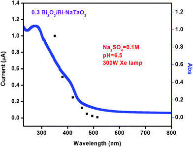
Fig. 14 shows the photoresponse spectra of 0.3 Bi2O3/Bi–NaTaO3 with various cut-off wavelengths of incident light. These data were obtained by irradiating samples via appropriate cut-off filters for the wavelength shown, i.e. photon counts decrease upon increasing wavelength. From the spectra, we observe there is generation of appreciable photocurrent for wavelengths below 525 nm. As was observed from the figure, no photocurrent was observed when the sample was irradiated at wavelengths longer than 525 nm, which is consistent with the absorption edge shown in Fig. 2. Maximum photocurrent is generated when light is irradiated with λ ≥ 350 nm. The generation of photocurrent gradually decreases with increasing cut-off wavelengths. This indicates that the photocurrent generated by the electrode is due to the visible light response of the system.
 |
| | Fig. 14 The dependence of photocurrent 0.3 Bi2O3/Bi–NaTaO3 irradiation wavelength. The DRUV-vis spectrum is also shown by the solid line. | |
3.8. Photocatalytic reaction over Bi2O3/Bi–NaTaO3
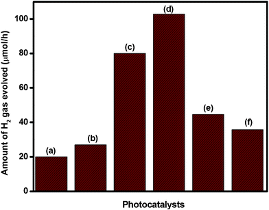
Fig. 15 shows the photocatalytic activities for hydrogen production over NaTaO3, Bi–NaTaO3, Bi2O3 and Bi2O3/Bi–NaTaO3 in aqueous methanol solution. Blank experiments showed no appreciable H2 evolution in the absence of either irradiation or photocatalyst. Neat NaTaO3, Bi–NaTaO3 are inactive under visible light irradiation due to the large bandgap energy. Photocatalytic H2 production over Bi2O3 and Bi2O3/Bi–NaTaO3 photocatalysts were evaluated under visible light illumination (λ ≥ 400 nm). It was already reported that some of the lower band gap materials such as BiOI and Bi2O3 effectively sensitized higher band gap materials like TiO2 and ZnO and enhanced their activity in the visible region.57,58,60 In the case of Bi2O3/Bi–NaTaO3, Bi2O3 nanoparticles played a vital role in the visible light-induced photocatalytic activity of Bi–NaTaO3, Bi2O3 being an inorganic photosensitizer having a band gap of 2.8 eV.61 It could be predicted that Bi2O3 nanoparticles might promote a photosensitizing effect which leads to enhanced activity in the visible region. Bi2O3 nanoparticles could be easily activated by visible light and induced photoelectrons and holes. In the absence of Bi–NaTaO3, these electrons and holes might recombine rapidly owing to the narrow energy gap, leading to the quenching of spectral response.62 The PEC measurement reveals that Bi2O3 is a p-type semiconductor and Bi–NaTaO3 is an n-type semiconductor. When they contact with each other, a junction is formed between them and the photoexcited electrons in the conduction band of the p-type Bi2O3 can be easily transferred to the n-type Bi–NaTaO3. This results in proficient transfer of charge carriers at the composite interface (Scheme 1(b)). Thus, the recombination of the charge carriers could be effectively suppressed and lead to higher photocatalytic activity. It is clear that the photocatalytic activity depended markedly on Bi concentration, and the catalyst prepared with the optimum amount of Bi concentration, i.e. 0.3 Bi2O3/Bi–NaTaO3, showed the highest activity. At this optimum Bi concentration, the photocatalyst was able to evolve 102.5 μmol h−1 of H2 gas. Higher concentrations of Bi result in agglomeration of Bi2O3 nanoparticles on the surface of Bi–NaTaO3, and could effectively inhibit the light absorption by photocatalytically active Bi–NaTaO3. To confirm the high charge transfer or low electron–hole recombination rate, photoluminescence (PL) studies have been undertaken. It is known that the PL emission results from the recombination of excited electrons and holes. Thus, the lower PL intensity indicates a lower recombination rate.37Fig. 9 showed the PL spectra of Bi2O3/Bi–NaTaO3. From the PL spectra, it was observed that 0.3 Bi2O3/Bi–NaTaO3 showed lowest blue luminescence intensity, indicating a lower recombination rate of photoinduced charge carriers compared with other photocatalysts. Higher Bi concentrations abruptly decrease the photocatalytic activity of the photocatalysts. At higher concentrations of Bi (>0.3 molar ratio), the photocatalytic activity of Bi2O3/Bi–NaTaO3 is hindered, even though the absorption onset of the photocatalysts is shifted towards the red region. The higher amount of Bi-species results in the formation of defect states and unwanted formation of impurities such as BiTaO4, due to large amounts of bismuth incorporated into the NaTaO3 lattice. The creation of defect states and unwanted phase formation acts as a recombination centre, which predominantly hinders the photocatalytic activity of the present investigated system.
 |
| | Fig. 15 Photocatalytic hydrogen evolution over (a) Bi2O3 (b) 0.1 Bi2O3/Bi–NaTaO3 (c) 0.2 Bi2O3/Bi–NaTaO3 (d) 0.3 Bi2O3/Bi–NaTaO3 (e) 0.4 Bi2O3/Bi–NaTaO3 (f) 0.5 Bi2O3/Bi–NaTaO3 in aqueous methanol solution. | |
4. Conclusions
The present study provides a new approach to synthesize Bi2O3/Bi–NaTaO3 photocatalysts through a low temperature solid state reaction method. At low bismuth concentrations, the incorporated bismuth doped into the NaTaO3 lattice, but at higher concentrations, the excess bismuth forms its oxide and remains as a separate phase. The FESEM confirmed the deposition of Bi2O3 particles on the surface of Bi–NaTaO3 which is consistent with TEM micrographs. The lowest PL intensity was observed in the case of 0.3 Bi2O3/Bi–NaTaO3, indicating the effective separation of photogenerated charge carriers. Bi concentrations greater than the optimum (>0.3 molar ratio) value result in the formation of defect states and impurities such as BiTaO4, which decreases the photocatalytic activity. The PEC measurement confirmed the n-type character of Bi–NaTaO3 and the p-type character of Bi2O3. The p–n junction between Bi2O3 and Bi–NaTaO3 effectively suppresses the electron–hole recombination and enhances the photocatalytic activity. The 0.3 Bi2O3/Bi–NaTaO3 photocatalyst exhibits the highest performance of H2 evolution, 102.5 μmol h−1 in aqueous methanol solution under visible light irradiation (λ ≥ 400 nm).
Acknowledgements
The authors are very grateful to Prof. B.K. Mishra, Director, IMMT, Bhubaneswar for giving permission to publish the work. The financial assistance by CSIR for funding a Networking Project (NWP 22) is greatly acknowledged. The authors are very grateful to Prof. K. Domen and Dr T. Minegishi (University of Tokyo, Japan) for their valuable suggestions regarding this work and for photoelectrochemical measurement studies, and Mr. M. Moriya for performing XPS analyses. The support from DST and JSPS is greatly acknowledged for the INDO-JAPAN collaborative project. The authors K. H. Reddy and S. Martha are thankful to CSIR, New Delhi for SRF.
References
- J. S. Lee, Catal. Surv. Asia, 2005, 9, 4 CrossRef.
- R. Marschall, A. Mukherji, A. Tanksale, C. Sun, S. C. Smith, L. Wang and G. Q. Lu, J. Mater. Chem., 2011, 21, 8871 RSC.
- A. Fujishima and K. Honda, Nature, 1972, 238, 37 CrossRef CAS.
- H. Tong and J. Ye, Eur. J. Inorg. Chem., 2010, 1473 CrossRef CAS.
- A. Kudo and H. Kato, Chem. Lett., 1997, 867 CrossRef CAS.
- H. Kato and A. Kudo, Chem. Phys. Lett., 1998, 295, 487 CrossRef CAS.
- H. Kato and A. Kudo, Chem. Lett., 1999, 1207 CrossRef CAS.
- A. Kudo, H. Okutomi and H. Kato, Chem. Lett., 2000, 1212 CrossRef CAS.
- D. W. Hwang, H. G. Kim, J. Kim, K. Y. Cha and J. S. Lee, J. Catal., 2000, 193, 40 CrossRef CAS.
- A. Kudo, H. Kato and S. J. Nkagawa, J. Phys. Chem. B, 2000, 104, 571 CrossRef CAS.
- K. Sayama, H. Arakawa and K. Domen, Catal. Today, 1996, 28, 175 CrossRef CAS.
- T. Ishihara, H. Nishiguchi, K. Fukamachi and Y. Takkkita, J. Phys. Chem. B, 1999, 103, 1 CrossRef CAS.
- M. Machida, J. Yabunaka and T. Kijima, Chem. Mater., 2000, 12, 812 CrossRef CAS.
- X. Li and J. Zang, J. Phys. Chem. C, 2009, 113, 19411 CAS.
- H. Kato, K. Asakura and A. Kudo, J. Am. Chem. Soc., 2003, 125, 3082 CrossRef CAS.
- J. Xu, D. Xue and C. Yan, Mater. Lett., 2005, 59, 2920 CrossRef CAS.
- D. Tiwari and S. Dunn, J. Mater. Sci., 2009, 44, 5063 CrossRef CAS.
- J. L. Giocondi and G. S. Rohrer, Chem. Mater., 2001, 13, 241 CrossRef CAS.
- S. V. Kalinin, D. A. Bonnell, T. Alvarez, X. Lei, Z. Hu, J. H. Ferris, Q. Zhang and S. Dunn, Nano Lett., 2002, 2, 586 CrossRef.
- Y. Zhang, A. M. Schultz, P. A. Salvador and G. S. Rohrer, J. Mater. Chem., 2011, 21, 4168 RSC.
- Z. G. Yi and J. H. Ye, J. Appl. Phys., 2009, 106, 074910 CrossRef.
- M. Yang, X. Huang, S. Yan, Z. Li, T. Yu and Z. Zou, Mater. Chem. Phys., 2010, 121, 506 CrossRef CAS.
- Z. G. Yi and J. H. Ye, Appl. Phys. Lett., 2007, 91(254108), 1 Search PubMed.
- D. R. Liu, C. D. Wei, B. Xue, X. G. Zhang and Y. S. J. Jiang, J. Hazard. Mater., 2010, 182, 50 CrossRef CAS.
- H. Fu, S. Zhang, L. Zhang and Y. Zhu, Mater. Res. Bull., 2008, 43, 864 CrossRef CAS.
- A. Iwase, K. Saito and A. Kudo, Bull. Chem. Soc. Jpn., 2009, 82, 514 CrossRef CAS.
- Z. Li, Y. Wang, J. Liu, G. Chen, Y. Li and C. Zhou, Int. J. Hydrogen Energy, 2009, 34, 147 CrossRef CAS.
- X. Wang, H. Bai1, Y. Meng, Y. Zhao, C. Tang and Y. Gao, J. Nanosci. Nanotechnol., 2010, 10, 1788 CrossRef CAS.
- P. D. Kanhere, J. Zheng and Z. Chen, J. Phys. Chem. C, 2011, 115, 11846 CAS.
- A. E. Morales, M. H. Zaldivar and U. Pal, Opt. Mater., 2006, 29, 100 CrossRef.
- H. Lin, C. P. Huang, W. Li, C. Ni, S. I. Shah and Y. H. Tseng, Appl. Catal., B, 2006, 68, 1 CrossRef CAS.
- K. M. Parida, K. H. Reddy, S. Martha, D. P. Das and N. Biswal, Int. J. Hydrogen Energy, 2010, 35, 12161 CrossRef CAS.
- D. Li, J. Zheng, Z. Li, X. Fan, L. Liu and Z. Zou, Int. J. Photoenergy, 2007, 21680, 7, DOI:10.1155/2007/21860.
- C. C. Hu, Y. L. Lee and H. Teng, J. Mater. Chem., 2011, 21, 3824 RSC.
- A. Kudo, K. Omori and H. Kato, J. Am. Chem. Soc., 1999, 121, 11459 CrossRef CAS.
- B. Y. Lee, S. H. Park, S. C. Lee, M. Kang, C. H. Park and S.-J. Choung, Korean J. Chem. Eng., 2003, 20, 812 CrossRef CAS.
- K. M. Parida, S. Martha, D. P. Das and N. Biswal, J. Mater. Chem., 2010, 20(7144), 29 Search PubMed.
- M. Maruyama, A. Iwase, H. Kato, A. Kudo and H. Onishi, J. Phys. Chem. C, 2009, 113, 13918 CAS.
- Y. C. Lee, H. Teng, C. C. Hu and S. Y. Hu, Electrochem. Solid-State Lett., 2008, 11, P1 CrossRef CAS.
- S. Cabuk, H. Akkus and A. M. Mamedov, Phys. B, 2007, 394, 81 CrossRef CAS.
- R. Leonelli and J. L. Brebner, Phys. Rev. B, 1986, 33, 8649 CrossRef CAS.
- M. Aguilar and F. Agullo-Lopez, J. Appl. Phys., 1982, 53, 9009 CrossRef CAS.
- T. Hasegawa, M. Shirai and K. Tanaka, J. Lumin., 2000, 87, 1217 CrossRef.
- V. A. Trepakov, V. S. Vikhnin, S. Kapphan, L. Jastrabik, J. Licher and P. P. Syrnikov, J. Lumin., 2000, 87, 1126 CrossRef.
- V. V. Laguta, M. D. Glinchuk, I. P. Bykov, A. Cremona, P. Galinetto, E. Giulotto, L. Jastrabik and J. Rosa, J. Appl. Phys., 2003, 93, 6056 CrossRef CAS.
- S. E. Kapphan, A. I. Gubaev and V. S. Vikhnin, Phys. Status Solidi C, 2005, 2, 128 CrossRef CAS.
- Y. Lee, T. Watanabe, T. Takata, J. N. Kondo, M. Hara, M. Yoshimura and K. Domen, Chem. Mater., 2005, 17, 2422 CrossRef CAS.
- J. K. Reddy, B. Srinivas, V. Durga Kumari and M. Subrahmanyam, Chem. Cat. Chem., 2009, 1, 492 Search PubMed.
- R. S. Devan, W. D. Ho, C. H. Chen, H. W. Shiu, C. H. Ho, C. L. Cheng, S. Y. Wu, Y. Liou and Y. R. Ma, Nanotechnology, 2009, 20(445708), 5pp Search PubMed.
- K. Chen, G. R. Yang, M. Nielsen, T. M. Lu and E. Rymaszewski, J. Appl. Phys. Lett., 1997, 70, 399 CrossRef CAS.
- E. Atanassova and D. Spassov, Appl. Surf. Sci., 1998, 135, 71 CrossRef CAS.
- O. Kerrec, D. Devilliers, H. Groult and P. Marcus, Mater. Sci. Eng., B, 1998, 55, 134 CrossRef.
- E. Atanassova, G. Tyuliev, A. Paskaleva, D. Spassov and K. Kostov, Appl. Surf. Sci., 2004, 225, 86 CrossRef CAS.
- D. W. Hwang, J. Kim, T. J. Park and J. S. Lee, Catal. Lett., 2002, 80, 53 CrossRef CAS.
- K. M. Parida, A. Nashim and S. K. Mahanta, Dalton Trans., 2011, 40, 12839 RSC.
- H. G. Kim, P. H. Borse, J.S. Jang, E. D. Jeong, O. S. Jung, Y. J. Suhd and J. S. Lee, Chem. Commun., 2009, 5889 RSC.
- J. Jiang, X. Zhang, P. Sun and L. Zhang, J. Phys. Chem. C, 2011, 115, 20555 CAS.
- G. Dai, J. Yu and G. Liu, J. Phys. Chem. C, 2011, 115, 7339 CAS.
- H. Chen, L. Hu, X. Fang and L. Wu, Adv. Funct. Mater., 2012, 22, 1229 CrossRef CAS.
- B. Naik, S. Martha and K. M. Parida, Int. J. Hydrogen Energy, 2011, 36, 2794 CrossRef CAS.
- J. Zhu, S. Wang, J. Wang, D. Zhang and H. Li, Appl. Catal., B, 2011, 102, 120 CrossRef CAS.
- Z. Bian, J. Zhu, S. Wang, Y. Cao, X. Qian and H. Li, J. Phys. Chem. C, 2008, 112, 6258 CAS.
|
| This journal is © The Royal Society of Chemistry 2012 |
Click here to see how this site uses Cookies. View our privacy policy here. ![[thin space (1/6-em)]](https://www.rsc.org/images/entities/char_2009.gif) :
:![[thin space (1/6-em)]](https://www.rsc.org/images/entities/char_2009.gif) NaTaO3, with a perovskite structure, has been proven to be one of the most promising photocatalysts for water splitting reactions with a highest quantum efficiency of 56% at λ = 270 nm.15 Sodium tantalate is an important lead-free perovskite-type ferroelectric material.16 Over the last few years, researchers have paid much attention to the use of ferroelectric materials as photocatalysts.17–19 Ferroelectric materials have internal dipolar fields which can drive photogenerated electrons and holes in opposite directions and hence reduce the electron–hole recombination. The minimisation of electron–hole recombination in the materials greatly enhances the photocatalytic efficiency.20 However, pure NaTaO3 becomes active solely under ultraviolet light, which is only a small part (4%) of solar irradiation. But this material might be a good mother structure for design and development of visible light driven photocatalysts. A number of different attempts have been made to modify NaTaO3 in order to make it active in the visible light region, mainly by doping with cations or anions.21,24 To date, NaTaO3 based visible-light-driven photocatalysts are rare. Recently, some reports have been found on the development of visible-light-driven NaTaO3-based photocatalysts such as Na1−xLaxTa1−xCrxO3,21,22 Na1−xLaxTa1−xCoxO3,23 NaTaO3−xNx,24,25 Ir-La-doped NaTaO3etc.26 Therefore, it is of great interest to develop novel visible-light responsive NaTaO3 photocatalysts. Recently, bismuth-doped NaTaO3 nanoparticles prepared by a hydrothermal method have been studied for photocatalytic reactions. Li et al. reported a visible light active solid solution photocatalyst, i.e. NaTa1−xBixO3. Hydrogen evolution over these nanoparticles was reported without any co-catalyst loading under visible light radiation.27 The optical absorption properties of Bi3+-doped NaTaO3 nanoparticles were also studied by Wang et al., where a small change in the absorption edge of NaTaO3 was observed upon Bi doping.28 Kanhere et al. have studied the effects of Bi doping on Na or Ta or both Na and Ta sites and their optical and photocatalytic decomposition of methylene blue.29 However, there have been no reports so far on Bi2O3/Bi–NaTaO3 and their optical properties and photocatalytic activity towards H2 evolution from aqueous methanol solution. Therefore, detailed investigations on the optical properties and photocatalytic production of hydrogen over Bi2O3/Bi–NaTaO3 powders with different concentrations of Bi are necessary.
NaTaO3, with a perovskite structure, has been proven to be one of the most promising photocatalysts for water splitting reactions with a highest quantum efficiency of 56% at λ = 270 nm.15 Sodium tantalate is an important lead-free perovskite-type ferroelectric material.16 Over the last few years, researchers have paid much attention to the use of ferroelectric materials as photocatalysts.17–19 Ferroelectric materials have internal dipolar fields which can drive photogenerated electrons and holes in opposite directions and hence reduce the electron–hole recombination. The minimisation of electron–hole recombination in the materials greatly enhances the photocatalytic efficiency.20 However, pure NaTaO3 becomes active solely under ultraviolet light, which is only a small part (4%) of solar irradiation. But this material might be a good mother structure for design and development of visible light driven photocatalysts. A number of different attempts have been made to modify NaTaO3 in order to make it active in the visible light region, mainly by doping with cations or anions.21,24 To date, NaTaO3 based visible-light-driven photocatalysts are rare. Recently, some reports have been found on the development of visible-light-driven NaTaO3-based photocatalysts such as Na1−xLaxTa1−xCrxO3,21,22 Na1−xLaxTa1−xCoxO3,23 NaTaO3−xNx,24,25 Ir-La-doped NaTaO3etc.26 Therefore, it is of great interest to develop novel visible-light responsive NaTaO3 photocatalysts. Recently, bismuth-doped NaTaO3 nanoparticles prepared by a hydrothermal method have been studied for photocatalytic reactions. Li et al. reported a visible light active solid solution photocatalyst, i.e. NaTa1−xBixO3. Hydrogen evolution over these nanoparticles was reported without any co-catalyst loading under visible light radiation.27 The optical absorption properties of Bi3+-doped NaTaO3 nanoparticles were also studied by Wang et al., where a small change in the absorption edge of NaTaO3 was observed upon Bi doping.28 Kanhere et al. have studied the effects of Bi doping on Na or Ta or both Na and Ta sites and their optical and photocatalytic decomposition of methylene blue.29 However, there have been no reports so far on Bi2O3/Bi–NaTaO3 and their optical properties and photocatalytic activity towards H2 evolution from aqueous methanol solution. Therefore, detailed investigations on the optical properties and photocatalytic production of hydrogen over Bi2O3/Bi–NaTaO3 powders with different concentrations of Bi are necessary.
![[thin space (1/6-em)]](https://www.rsc.org/images/entities/char_2009.gif) :
:![[thin space (1/6-em)]](https://www.rsc.org/images/entities/char_2009.gif) [Bi]
[Bi]![[thin space (1/6-em)]](https://www.rsc.org/images/entities/char_2009.gif) :
:![[thin space (1/6-em)]](https://www.rsc.org/images/entities/char_2009.gif) [Ta] = 1 − x
[Ta] = 1 − x![[thin space (1/6-em)]](https://www.rsc.org/images/entities/char_2009.gif) :
:![[thin space (1/6-em)]](https://www.rsc.org/images/entities/char_2009.gif) x
x![[thin space (1/6-em)]](https://www.rsc.org/images/entities/char_2009.gif) :
:![[thin space (1/6-em)]](https://www.rsc.org/images/entities/char_2009.gif) 1 (where x = 0–0.5) followed by the addition of urea (SDS AR, purity 99.5%) powder. In the present study, the molar ratio of urea to metal ions was kept at [urea]
1 (where x = 0–0.5) followed by the addition of urea (SDS AR, purity 99.5%) powder. In the present study, the molar ratio of urea to metal ions was kept at [urea]![[thin space (1/6-em)]](https://www.rsc.org/images/entities/char_2009.gif) :
:![[thin space (1/6-em)]](https://www.rsc.org/images/entities/char_2009.gif) [Na2C2O4 + Bi (NO3)3·5H2O + Ta2O5] = 2
[Na2C2O4 + Bi (NO3)3·5H2O + Ta2O5] = 2![[thin space (1/6-em)]](https://www.rsc.org/images/entities/char_2009.gif) :
:![[thin space (1/6-em)]](https://www.rsc.org/images/entities/char_2009.gif) 1. The mixtures (Ta2O5, Na2C2O4, Bi(NO3)3·5H2O and urea) were ground thoroughly in a mortar and transferred into a crucible. Then the mixture was activated in a muffle furnace with the heating rate of 2 °C min−1 ranging from room temperature to 300 °C, 5 °C min−1 ranging from 300 to 600 °C and kept at 600 °C for 4 h. For simplicity, Bi doped NaTaO3 prepared at a Bi concentration of 0.05 molar ratio is designated as Bi–NaTaO3 and Bi2O3/Bi–NaTaO3 photocatalysts prepared by varying the bismuth concentration from 0.1–0.5 molar ratio are designated as 0.1 Bi2O3/Bi–NaTaO3, 0.2 Bi2O3/Bi–NaTaO3, 0.3 Bi2O3/Bi–NaTaO3, 0.4 Bi2O3/Bi–NaTaO3, 0.5 Bi2O3/Bi–NaTaO3 respectively. The Bi2O3 was also prepared by same method.
1. The mixtures (Ta2O5, Na2C2O4, Bi(NO3)3·5H2O and urea) were ground thoroughly in a mortar and transferred into a crucible. Then the mixture was activated in a muffle furnace with the heating rate of 2 °C min−1 ranging from room temperature to 300 °C, 5 °C min−1 ranging from 300 to 600 °C and kept at 600 °C for 4 h. For simplicity, Bi doped NaTaO3 prepared at a Bi concentration of 0.05 molar ratio is designated as Bi–NaTaO3 and Bi2O3/Bi–NaTaO3 photocatalysts prepared by varying the bismuth concentration from 0.1–0.5 molar ratio are designated as 0.1 Bi2O3/Bi–NaTaO3, 0.2 Bi2O3/Bi–NaTaO3, 0.3 Bi2O3/Bi–NaTaO3, 0.4 Bi2O3/Bi–NaTaO3, 0.5 Bi2O3/Bi–NaTaO3 respectively. The Bi2O3 was also prepared by same method.
