Graphene–carbon nanotube composite as an effective conducting scaffold to enhance the photoelectrochemical water oxidation activity of a hematite film†
Jae
Young Kim‡
,
Ji-Wook
Jang‡
,
Duck
Hyun Youn
,
Jae
Yul Kim
,
Eun
Sun Kim
and
Jae
Sung Lee
*
Department of Chemical Engineering, Division of Advanced Nuclear Engineering, Pohang University of Science and Technology (POSTECH), San 31, Hyoja-dong, Pohang 790784, Republic of Korea. E-mail: jlee@postech.ac.kr; Fax: 82 54 279 5528; Tel: 82 54 279 8272
First published on 8th August 2012
Abstract
The iron oxide photoanode was modified with a graphene–carbon nanotube (CNT) composite conducting scaffold for efficient charge transfer from Fe2O3 particles to transparent conducting oxide substrate in photoelectrochemical water splitting cells. The Fe2O3–composite photoanode showed a photocurrent increase of 530% compared with to the bare Fe2O3 photoanode at 1.23 V vs. RHE, while the increase was only 200 and 240% for Fe2O3–CNT and Fe2O3–graphene photoanodes, respectively. This remarkable performance enhancement by the composite scaffold was attributed to synergistic effects induced by the formation of a 3D-like architecture from 1D CNT and 2D graphene. They become a spacer for each other forming a more open and highly exposed structure, in which both 2D graphene and 1D CNT can exist in the forms with much less self-agglomeration, thus not only enlarging the contact area between the conducting scaffold and Fe2O3 particles but also recovering in part the intrinsic conducting ability of graphene and CNT.
Introduction
Photoelectrochemical (PEC) water splitting is an efficient and environmentally-friendly method to produce hydrogen from water using solar light.1 A typical PEC cell contains a working photoanode (usually made of an n-type semiconductor film) that absorbs light to oxidize water and produce gaseous oxygen, protons, and photo-excited electrons.| 2H2O (l) + hv → O2 (g) + 4H+ + 4e− | (1) |
The formed photoelectrons (e−) are collected in the transparent conducting oxide (TCO) glass and sent to a counter cathode (usually made of a metal or a p-type semiconductor) via an external circuit. In the cathode, gaseous hydrogen is produced to complete overall water splitting.
| 2H+ + 2e− → H2 (g) | (2) |
The fabrication of the photoelectrode materials is the key to the successful construction of a high efficiency PEC cell. Iron oxide, usually αFe2O3 (or hematite), has been studied extensively as a semiconductor photoanode material because of its narrow band gap (2.1 eV) that allows absorption of a large fraction (ca. 13.5%) of solar light, stability in alkaline solutions, low cost, and environmentally benign characters.2,3a However, its poor charge transport property (hole diffusion length of ca. 4 nm) has been a serious drawback that reduces its efficiency in water oxidation. A strategy to improve the charge transport property of semiconductors is its modification with conducting materials such as carbon nanotubes (CNT)3 or the new material, graphene.4 As a conducting scaffold, CNT or graphene are expected to provide an expressway of electron transport from the semiconductor to the charge collector, i.e. a TCO substrate.
In most cases, however, the excellent properties of CNT or graphene are not revealed in practical applications because of severe self-agglomeration of these 1D and 2D carbon materials. Thus, their fabrication into macroscopic 3D structures is essential for many applications.5 Recently, the composite of graphene–CNT has received great attention in various energy devices due to synergistic effects of these two carbon materials on its structural, conducting, and textural properties. Thus, highly conductive free-standing graphene–CNT composite films were developed.6a By combining 2D graphene and 1D CNT, a synergistic effect in conductivity was established. Self-assembled graphene–CNT composite films were also demonstrated to possess an interconnected network of carbon structures with well-defined nanopores suitable for supercapacitors.6b Graphene–CNT composite materials were reported to have a small square resistance and high transmittance relative to pure carbon materials, and could become high-performance transparent conductors.6c,d We have realized that these properties are also highly desirable for photoelectrodes of PEC cells. Thus, here we apply for the first time this concept of 3D-like carbon structure fabrication with a graphene–CNT composite to a conducting scaffold of PEC cell systems.
In our previous study,3a we prepared an αFe2O3 photoanode modified with multi-wall CNT to facilitate electron passage from the semiconductor to TCO substrate for PEC water splitting under sun light. Indeed, the CNT-modified Fe2O3 electrode exhibited increased efficiency relative to the unmodified Fe2O3 electrode. Now, we introduce the graphene–CNT composite as a new type of conducting scaffold for Fe2O3 particles. As a charge transfer expressway, the graphene–CNT composite scaffold is expected to have several advantages. In a pure carbon conducting scaffold, graphene sheets or CNTs are easily agglomerated due to the repetition of the same structure (2D for graphene sheets and 1D for CNT). As a result, the contact area between the scaffold and Fe2O3 particles is reduced and the conducting property also gets deteriorated caused by the agglomeration, increased edges, surface boundaries, and other possible factors. As mentioned, there have been many experimental observations6a–d that show a dramatic decrease of sheet resistance of graphene–CNT composite films relative to either graphene or CNT films. According to a theoretical analysis,6e the conductivity of polycrystalline graphene is limited by high resistance grain boundaries. In the graphene–CNT composite, the CNT offers a ‘sub-percolating’ conducting network that bridges the percolation bottleneck, i.e. the grain boundaries of the graphene sheet. When we form a well-dispersed composite between graphene and CNT, they could act like a spacer for each other. In other words, CNT can be a spacer to exfoliate graphene sheets and vice versa. The concept of the spacer has been recently invoked in a carbon black–graphene system, where carbon black particles separate graphene sheets to help the single sheet graphene recover its original properties.7 Thus, the excellent conducting properties of graphene and CNT could be manifested in their composite structure. In addition, we found that the pure graphene thin film was easily peeled off from a TCO substrate in electrolyte. Thus, the composite could also play the role of a binder to prepare a robust thin semiconductor film.
Scheme 1 and the small schematic diagrams in Fig. 1 illustrate these concepts in the conducting scaffolds. The 2D pure graphene scaffold (A) with an agglomerated flat structure can contact only the bottom part of the Fe2O3 particle layers. The 1D pure CNT scaffold (B) allows a little better contact than the graphene scaffold, but CNT are also easily entangled each other, hampering the contact with Fe2O3 particles. The graphene–CNT composite scaffold (C) forms a 3D-like architecture using the counterpart structures as mutual spacers. In this architecture, both 2D graphene and 1D CNT can be more uniformly dispersed without serious self-agglomeration due to the spacer role of graphene and CNT for each other. It can accommodate a larger number of Fe2O3 particles to its contact since the composite scaffold has a more loose structure with the high exposed area. The graphene–CNT composite will provide an excellent conducting scaffold for charge transfer from Fe2O3 particles to a TCO substrate by enlarging the contact area between the scaffold and Fe2O3 particles and recovering in part the excellent conducting ability of graphene and CNT. In the present work, this concept will be verified experimentally in the fabrication of efficient photoelectrodes.
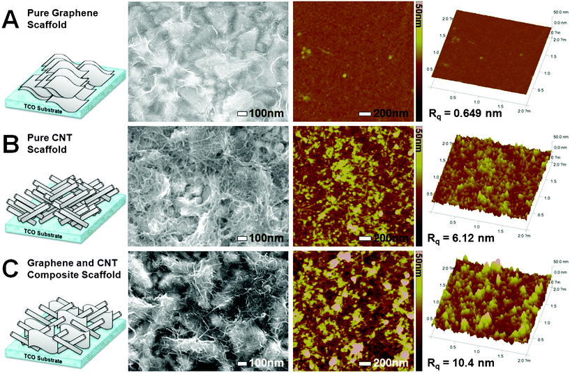 | ||
| Fig. 1 Surface SEM, AFM images, and 3D surface AFM images of the pure graphene (A), CNT (B), and graphene–CNT composite (C) scaffold deposited on TCO substrate. 2D and 3D surface AFM images were taken from the same area (2 × 2 μm2). | ||
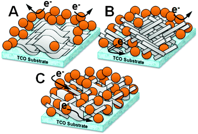 | ||
| Scheme 1 Iron oxide photoanodes modified with the conducting scaffolds of pure graphene (A), CNT (B), and graphene–CNT composite (C). | ||
Experimental
Preparation of graphene dispersion for spray coating
The Fe2O3 photoanodes modified with a conducting scaffold were prepared using a simple two-step process; spray coating of the conducting scaffold followed by electron beam evaporation and calcination of iron particles. A high intensity ultrasonic processor (750 W-model, Autotune Series) was used to ultrasonicate 55 mg graphene oxide (GO, made by Hummer's method7b) in 55 mL water for 30 min. The solution was centrifuged at 3000 rpm for 30 min (MF500, Hanil). 50 mL of GO solution was diluted with 50 mL of distilled water containing 50 μL of hydrazine solution (35 wt%, Aldrich) and 250 μL of ammonia solution (∼30%). After vigorous mixing for a few minutes, the solution was maintained for 3 h at 95 °C.7c The solubility of reduced graphene oxide was ∼0.3 mg mL−1.Preparation of CNT and graphene dispersions for spray coating
The multi-wall CNT was purchased from Hanwha Nanotech Corporation (Korea) with a diameter of 3 nm and was refluxed in 6 M nitric acid at 120 °C for 16 h. The resultant solution was washed with an excess amount of distilled water. Acid treated CNT remaining on the filter was carefully removed from the filter after drying, and redispersed in distilled water (0.3 mg mL−1). The graphene dispersion and CNT dispersion was mixed with 2-propanol with 1![[thin space (1/6-em)]](https://www.rsc.org/images/entities/char_2009.gif) :
:![[thin space (1/6-em)]](https://www.rsc.org/images/entities/char_2009.gif) 1 volume ratio of water and 2-propanol right before the spray coating to allow spray coating at a relatively low temperature of 100 °C. In order to deposit the total carbon amount of 0.1 mg on 1 cm2 FTO-coated glass substrate, the graphene–CNT mixtures of the various compositions (the ratios of 9
1 volume ratio of water and 2-propanol right before the spray coating to allow spray coating at a relatively low temperature of 100 °C. In order to deposit the total carbon amount of 0.1 mg on 1 cm2 FTO-coated glass substrate, the graphene–CNT mixtures of the various compositions (the ratios of 9![[thin space (1/6-em)]](https://www.rsc.org/images/entities/char_2009.gif) :
:![[thin space (1/6-em)]](https://www.rsc.org/images/entities/char_2009.gif) 1–1
1–1![[thin space (1/6-em)]](https://www.rsc.org/images/entities/char_2009.gif) :
:![[thin space (1/6-em)]](https://www.rsc.org/images/entities/char_2009.gif) 9) were tried to find an optimum mass ratio of graphene and CNT of 2
9) were tried to find an optimum mass ratio of graphene and CNT of 2![[thin space (1/6-em)]](https://www.rsc.org/images/entities/char_2009.gif) :
:![[thin space (1/6-em)]](https://www.rsc.org/images/entities/char_2009.gif) 3. The unmodified Fe2O3 electrode was prepared using the same method without the prior deposition of any scaffold.
3. The unmodified Fe2O3 electrode was prepared using the same method without the prior deposition of any scaffold.
Catalyst characterization and electrochemical studies
In order to characterize the Fe2O3 thin film and conducting scaffolds, X-ray diffraction (XRD) analysis (PW3040/60 X′pert PRO, PANalytical, with Cu–Kα (λ = 1.54056 Å) radiation), high resolution scanning electron microscopy (HRSEM, JSM-7401F, JEOL), and atomic force microscopy (AFM, MM07, Veeco) were used. The SEM images were taken from the carbon scaffold coated on FTO glass and AFM images from the carbon scaffold coated on mica substrate. The surface of the bare FTO glass is very rugged (Fig. S1†) while the surface of the mica substrate is almost perfectly flat. The electrode was put in a three electrode cell as a working photoanode to observe its photoelectrochemical water oxidation response. A platinum mesh electrode, Ag/AgCl electrode, and 1 M sodium hydroxide were also employed in the cell as a counter electrode, reference electrode, and electrolyte, respectively. Photocurrent–potential curves and electrochemical impedance spectra (EIS) were recorded under simulated solar light generated by a solar simulator (91![[thin space (1/6-em)]](https://www.rsc.org/images/entities/char_2009.gif) 160, Oriel) with an air mass 1.5 G filter. The light intensity of the solar simulator was calibrated to 1 sun (100 mW cm−2) using a reference cell certified by the National Renewable Energy Laboratories, U. S. Chronoamperometry for photocurrent stability testing and IPCE measurements were carried out on the same three electrode cell at 1.23 V vs. RHE. When IPCE was recorded, the cell was irradiated by a 300 W xenon lamp (66
160, Oriel) with an air mass 1.5 G filter. The light intensity of the solar simulator was calibrated to 1 sun (100 mW cm−2) using a reference cell certified by the National Renewable Energy Laboratories, U. S. Chronoamperometry for photocurrent stability testing and IPCE measurements were carried out on the same three electrode cell at 1.23 V vs. RHE. When IPCE was recorded, the cell was irradiated by a 300 W xenon lamp (66![[thin space (1/6-em)]](https://www.rsc.org/images/entities/char_2009.gif) 905, Oriel Instruments) coupled with a monochromator (74
905, Oriel Instruments) coupled with a monochromator (74![[thin space (1/6-em)]](https://www.rsc.org/images/entities/char_2009.gif) 004, Oriel Conerstone 130 1/8 m). A 299 nm cut-off filter was also placed at the exit of the output to prevent λ/2 radiation originated by Bragg diffraction at the grating. The EIS was recorded at DC potential of 1.23 V vs. RHE and an AC potential frequency range of 100
004, Oriel Conerstone 130 1/8 m). A 299 nm cut-off filter was also placed at the exit of the output to prevent λ/2 radiation originated by Bragg diffraction at the grating. The EIS was recorded at DC potential of 1.23 V vs. RHE and an AC potential frequency range of 100![[thin space (1/6-em)]](https://www.rsc.org/images/entities/char_2009.gif) 000–0.1 Hz with an amplitude of 10 mV. A potentiostat (IviumStat, Ivium Technologies) was used for applying bias potential to the cell and a software (ZView, Scribner Associates) was used for fitting the experimental EIS data to the equivalent circuit model. Mott-Schottky analysis was carried out at a DC potential range of 0.4–1.4 vs. RHE with an AC potential frequency 30 kHz under dark condition. The amplitude of AC potential was 10 mV.
000–0.1 Hz with an amplitude of 10 mV. A potentiostat (IviumStat, Ivium Technologies) was used for applying bias potential to the cell and a software (ZView, Scribner Associates) was used for fitting the experimental EIS data to the equivalent circuit model. Mott-Schottky analysis was carried out at a DC potential range of 0.4–1.4 vs. RHE with an AC potential frequency 30 kHz under dark condition. The amplitude of AC potential was 10 mV.
Results and discussion
Structure of the conducting scaffolds
Fig. 1 shows surface SEM and AFM images of the conducting scaffolds deposited on a TCO substrate (in the present study, fluorine-doped tin oxide (FTO) coated glass). The scaffold was deposited on the substrate using spray coating of aqueous dispersion of graphene (lateral dimensions of 200–500 nm) and/or CNT (diameter of 3 nm). The same amount of carbon (0.1 mg cm−2) was loaded on the substrate for all cases. Detailed experimental procedures including preparation of the graphene7b,c or CNT3a dispersions were described in the Experimental Section. In the SEM image of Fig. 1A, the pure graphene scaffold covers a rugged FTO surface like a cloth while in Fig. 1B, the pure CNT scaffold looks like a web. On the other hand, the graphene–CNT composite scaffold with an optimized mass ratio of 2![[thin space (1/6-em)]](https://www.rsc.org/images/entities/char_2009.gif) :
:![[thin space (1/6-em)]](https://www.rsc.org/images/entities/char_2009.gif) 3 forms a structure with an expanded surface area to contact Fe2O3 particles as much as possible. Note that the structure of the composite has been formed by a spontaneous self-assembly of two-types of carbons because they were obtained simply by mixing dispersions of graphene and CNT.
3 forms a structure with an expanded surface area to contact Fe2O3 particles as much as possible. Note that the structure of the composite has been formed by a spontaneous self-assembly of two-types of carbons because they were obtained simply by mixing dispersions of graphene and CNT.
The same tendency is observed in 2D and 3D AFM images. As one goes from the pure graphene, pure CNT to composite scaffold, the surface of the scaffolds becomes rougher. We checked root mean square roughness (Rq) of the scaffolds calculated from these AFM images. The Rq has a statistical significance since it describes the spread of the height distribution about the mean value of data points that exhibit Gaussian height distribution.8 The Rq values were 0.649, 6.12, and 10.4 nm for the pure graphene, CNT, and composite scaffolds, respectively. In addition, the average Rq values calculated from some 10 μm × 10 μm images (Fig. S2†) were 4.6, 22.5, and 28.6 nm (Rq statistically has a larger value for broader images).8 Therefore, the tendency is the same in the 2 μm × 2 μm images and 10 μm × 10 μm images. The surface of the graphene–CNT composite scaffold is rough enough over a broad area. The Rq values give us indirect information about the capacity that the conducting scaffold can accommodate Fe2O3 particles to its contact. We can expect the largest accommodation capacity and 3D characters for the graphene–CNT composite conducting scaffold based on its biggest standard deviation in height of surface points.
In order to confirm the dispersion state of the carbon nanomaterials, we carried out TEM analysis (JEM-2200FS with image Cs-corrector, JEOL) on the aqueous dispersions of pure graphene, pure CNT, and graphene–CNT composite as shown in Fig. 2. The aqueous dispersions of the same concentration (0.3 mg carbon mL−1) were used and the same amount (20 μL) was dropped on holey carbon grids of TEM. This procedure simulates the condition of scaffold fabrication of these carbon material films on FTO. As we can see clearly in the TEM images, graphene sheets and CNTs are less agglomerated in the graphene–CNT composite than CNT or graphene alone. In addition to the TEM images, a SAED pattern show 6 clear dots, which is consistent with the assumption that graphene monosheets can more easily exist in the graphene–CNT composite. On the other hand, we could not obtain a SAED pattern showing the 6 clear dots at any positions in pure graphene.
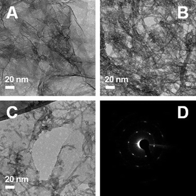 | ||
| Fig. 2 TEM images A: pure graphene, B: pure CNT, C: graphene–CNT composite, and D: SAED pattern for the image C. | ||
Thus, as we conjectured, the graphene–CNT composite scaffold forms a 3D-like architecture using the counterpart structures as mutual spacers. In this architecture, both 2D graphene and 1D CNT can be more uniformly dispersed without serious self-agglomeration because CNT separates graphene layers and graphene separates CNT bundles. Its loose and open 3D-like structure can accommodate a larger number of Fe2O3 particles to its contact than either graphene or CNT scaffolds. Both the enhanced contact capacity and improved conducting properties discussed later are desired for a conducting scaffold for more efficient semiconducting photoanodes.
Water oxidation activity of hematite films
Iron particles were deposited on the conducting scaffold using electron beam evaporation. After the deposition, the electrode was oxidized at 480 °C for 30 min in air to obtain Fe2O3 particles as a film on FTO glass. Thus, four types of the Fe2O3 electrodes were prepared: the bare Fe2O3, Fe2O3–graphene, Fe2O3–CNT, and Fe2O3–composite electrodes. XRD investigation revealed that highly crystalline α-phase Fe2O3 was well developed (Fig. 3A) by annealing in air. The composite films containing graphene and CNT remained transparent in all cases as the carbon-free Fe2O3 electrode (Fig. 3B). The optimized thickness of the electrode for the best performance under the current system was ca. 400 nm from trials of 100–1000 nm. Thus, as shown in Fig. 3C, the cross sectional SEM image of the Fe2O3–composte photoanode indicates that the 400 nm film has been formed on an FTO substrate of ca. 700 nm.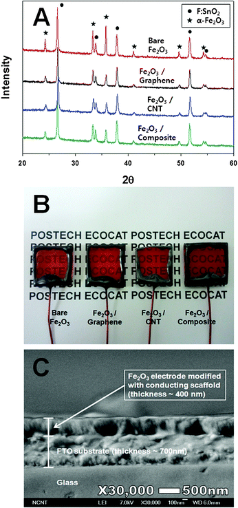 | ||
| Fig. 3 (A) XRD patterns of the electrodes; (B) photograph of the electrodes; (C) cross sectional SEM image of the Fe2O3 electrode modified with the graphene–CNT conducting scaffold. | ||
Now these hematite films were employed as photoanodes for photoelectrochemical (PEC) water oxidation. Fig. 4A shows the photocurrent responses of the photoanodes to an applied potential under simulated AM 1.5 G (1 sun) irradiation. The generated photocurrents are due to the transfer and collection of photoelectrons to the back Ohmic contact during the PEC water oxidation reaction caused by the valence band holes (eqn 1).
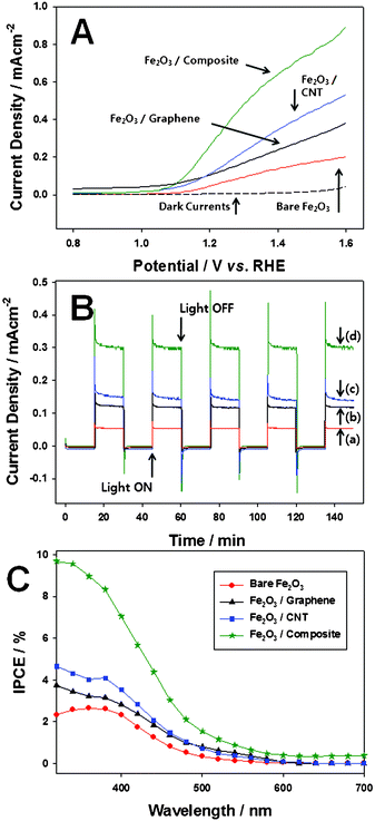 | ||
| Fig. 4 (A) Photocurrent vs. potential (I–V) characteristics curves for photoelectrochemical water with the photoanodes; (B) time-dependent photocurrent density (chronoamperometry) at 1.23 V vs. RHE applied bias potential; (a) bare Fe2O3, (b) Fe2O3–graphene, (c)Fe2O3–CNT, (d)Fe2O3–composite photoanode; (C) IPCE spectra of the photoanodes. | ||
For all photoanodes, the measured dark currents were negligible. Using gas chromatography analysis, it was confirmed that O2 and H2 (eqn 2) were produced at the photoanode and Pt mesh counter electrode, respectively. Under light irradiation, photocurrent was observed starting from 1.0 V vs. RHE for all the photoanodes. At 1.23 V vs. RHE (the theoretical potential necessary for water oxidation), the Fe2O3–graphene (122 mA cm−2), Fe2O3–CNT (145 mA cm−2), and Fe2O3–composite (325 mA cm−2) photoanodes show increased photocurrents by 200, 240, and 530%, respectively, compared with the bare Fe2O3 electrode (61 mA cm−2). The pure graphene and CNT conducting scaffolds undoubtedly improves PEC activity for water oxidation with Fe2O3 photoanodes due to their outstanding charge transfer property. However, their performance still remains at a somewhat low level caused by the structural limits of the pure carbon conducting scaffolds. Yet, the graphene–CNT composite conducting scaffold showed much more dramatic increases in the PEC activity. The graphene–CNT composite conducting scaffold increases the PEC activity by 270 and 220% even compared with the Fe2O3–graphene and Fe2O3–CNT photoanodes due to synergistic effects of graphene and CNT, i.e. by enlarging contact area between the conducting scaffold and Fe2O3 particles (confirmed by SEM and AFM), and recovering in part the original excellent conducting abilities of graphene and CNT (will be discussed in the next section with impedance responses of the photoanodes).
The time-dependent photocurrent generation (chronoamperometry) with 1.23 V vs. RHE applied bias potential is presented in Fig. 4B. The photocurrents responded exactly to the presence of light as the cell operation is interrupted for every 15 min (on/off cycle) and the steady state behavior of each photoanode followed the same trend of Fig. 4A. After the overshoot of current, the subsequent decay is determined by the rate at which minority carriers trapped at surface states capture majority carriers.9 At long times, the photocurrent approaches a steady state value that depends on the relative rates of recombination and charge transfer to redox species. The reason for the slower dynamic response in some electrodes could be ascribed to the slower rate which minority carriers trapped at surface states capture majority carriers possibly caused by the presence of the carbon scaffolds. However, the real reason may also be an unstable photocurrent when we consider long time scale used for the measurement of time-dependent photocurrent generation. The Fe2O3 electrodes modified with the carbon scaffold show the slow decay of photocurrent possibly due to some unstable mechanical, chemical or electrical conditions.
Incident photon to current conversion efficiency (IPCE) was measured for the photoanodes under irradiation with a 300 W xenon lamp coupled with a monochromator, and the results are displayed in Fig. 4C. For all photoanodes, IPCE value starts to increase around the incident light wavelength of 600 nm and it shows a good agreement with the known band gap of hematite, ∼2.1 eV. The Fe2O3–composite photoanode marks the best IPCE value over all wavelength regions indicating the graphene–CNT composite conducting scaffold constantly helps charge transfer and charge separation independent of photon energy that excited electrons. Of course this ability is much better than pure graphene and pure CNT conducting scaffold as clearly reflected in the IPCE spectra. The relative IPCE values for different electrodes closely follow the photocurrents displayed in Fig. 4A,B.
Electrochemical impedance studies
To elucidate the origin of the enhanced PEC water splitting activity of the Fe2O3 film with the graphene–CNT conducting scaffold, we performed a potentiostatic electrochemical impedance spectroscopy (EIS) study. Fig. 5A shows Nyquist plots of the photoanodes, where symbols represent experimental data and solid lines represent fitting results of these data to an equivalent RC circuit model in Fig. 5B, which consists of charge-transfer resistances (R) across the interfaces present in the photoanode and constant phase elements (CPE) in parallel. Single Nyquit plots for better observation of the shape of each Nyquist plot are also displayed in the supplementary information (Fig. S3†). The data for all electrodes were tried to fit to both 2-RC circuit and 3-RC circuit models. The model showing the best fit was chosen for the all electrodes. Thus, the bare Fe2O3 and Fe2O3–composite photoanodes were best fitted to a 3-RC circuit model while Fe2O3–graphene and Fe2O3–CNT to a 2-RC circuit model.T he assignment of an RC sub-circuit was done based on some criteria: time constant, consideration about the presence of the carbon scaffold at the Fe2O3|FTO interface, and results of previous studies.3a The table containing the calculated time constants is provided as Table S2.† In addition, a time constant represents a plateau point for one semicircle in the Nyquist plot, and at the same time, indirectly represents a reaction rate for a certain reaction occurring at one interface. Thus, the three RC circuits can be assigned to Fe2O3||electrolyte, Fe2O3 particles, and Fe2O3|FTO, respectively, i.e. the three major interfaces within the photoanode that predominantly develop impedance elements. In the next paragraph, each interface will be assigned to one RC sub-circuit and discussed further.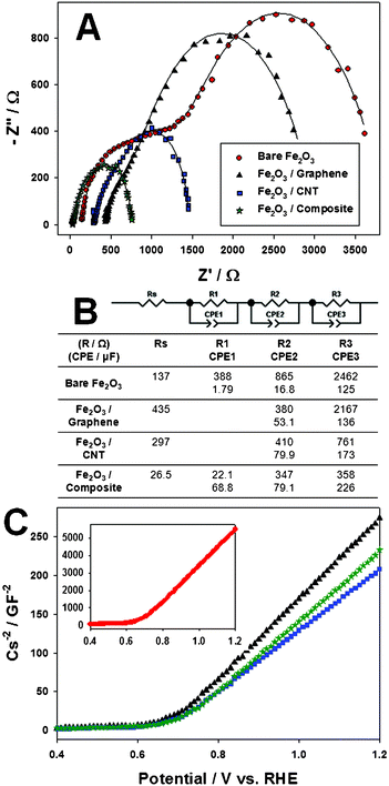 | ||
| Fig. 5 (A) Nyquist plots of the photoanodes; (B) the equivalent circuit model used for fitting the experimental data in A; (C) results from Mott–Schottky analysis conducted on the bare Fe2O3 (•), Fe2O3–graphene (▴), Fe2O3–CNT (■), and Fe2O3–composite (★) photoanode. | ||
First, the most difficult reaction in the photoanode, i.e. water oxidation, takes place at the Fe2O3||electrolyte interface, hence the biggest charge transfer resistance and double layer capacitance are generally observed here. In other words, the largest semicircle (R3/CPE3 sub-circuit in Fig. 4B) with the biggest charge transfer resistance and double layer capacitance usually corresponds to an n-type semiconductor||electrolyte interface in PEC systems. Next, we assume the second RC circuit originates from charge distribution over Fe2O3 particles. Charge transport here may represent the second most difficult part among reactions taking place within the Fe2O3 electrode due to its intrinsic poor conductivity and particle boundaries which can play the role of charge recombination sites. For the Fe2O3-composite photoanode, R3 is reduced by 6 times and CPE3 (an imperfect capacitor reflecting surface roughness, heterogeneity, etc.) increases 2 times relative to the bare Fe2O3 photoanodes, demonstrating water oxidation definitely occurs more easily under the promoted charge transfer environment by the graphene–CNT composite conducting scaffold. The effect is less pronounced for pure graphene or CNT scaffold. The pure graphene conducting scaffold is, to some degree, effective up to the bottom part of Fe2O3 particles as we can see that R2 decreases and CPE2 increases for the Fe2O3–graphene photoanode relative to bare Fe2O3. However, the improvement in its charge transfer ability barely reaches Fe2O3||electrolyte, and R3 and CPE3 do not change as much with pure graphene scaffold. The pure CNT scaffold works somewhat better than graphene but still not as effective as composite scaffold as we can see in relative R3 and CPE3 values. On the other hand, the graphene–CNT composite conducting scaffold is effective over the entire range of the photoanode from RS to the last RC circuit. The first RC circuit can be assigned to Fe2O3|FTO. As we expected, among the three major interfaces within the photoanode, Fe2O3|FTO inevitably has the smallest resistance or even negligible resistance value. We can interpret that the R1/CPE1 circuit does not exist for the Fe2O3–graphene and Fe2O3–CNT due to the negligible resistance value of the carbon scaffold. Both R1 (18 times decreased) and CPE1 (38 times increased) dramatically change after introduction of the composite scaffold relative to the bare Fe2O3 photoanode. Since the conducting scaffold is placed between Fe2O3 particles and FTO substrate, it is understandable that the dramatic change starts from Fe2O3|FTO and finally a greater number of holes can participate in water oxidation at Fe2O3||electrolyte.
Finally, RS (a left convergence point in the Nyquist plot) is generally referred to sheet resistance in a half cell test system for EIS.10 It increases for the Fe2O3 with the pure carbon scaffolds (graphene or CNT) compared with the bare Fe2O3 photoanode, because FTO alone shows lower resistance than graphene–FTO or CNT–FTO. This tendency was also observed in our previous study for Fe2O3 photoanodes with the pure CNT scaffold.3a On the other hand, RS decreases for the Fe2O3–composite photoanode to an even smaller value than the bare Fe2O3 photoanode employing FTO for its sole conducting part. Thus, the results demonstrate that the intrinsic conducting ability of graphene and CNT has been partly recovered in the composite scaffold, which is even better than that of FTO alone. As discussed, this is believed to be due to the spacer effect of graphene and CNT for each other.
Results of a Mott–Schottky analysis are presented in Fig. 5C. We can determine the flat band potential (EFB) and charge carrier density (N) of a semiconductor from this analysis.11 In brief, EFB and N can be calculated from the values of x-intercept and slope, respectively, when CS−2 (CS: capacitance for space charge layer) is plotted versus applied potential. The calculated EFB value was around 0.65 V vs. RHE for the bare Fe2O3 and 0.67 V vs. RHE for the Fe2O3 photoanode modified with the carbon conducting scaffold (graphene and/or CNT). The N value was very different between the bare Fe2O3 photoanode and the Fe2O3 photoanodes modified with the carbon conducting scaffolds. It was calculated to be 1.13 × 1016 cm−3 for the bare Fe2O3 photoanode and 2.27–2.98 × 1017 cm−3 for the the Fe2O3 photoanodes modified with the carbon conducting scaffolds. There was not a big change of EFB after introducing the carbon conducting scaffold into the Fe2O3 photoanode, whereas charge carrier density increased by ∼10 fold. Qualitatively similar results have been reported earlier for a ZnO–CNT system.11 In fact, there is no general reason that the carbon materials should increase charge carrier density of Fe2O3 film in the present system because they were hired as a conducting scaffold not as a dopant. However, the carbon conducting scaffold may affect the results of the Mott–Schottky analysis by its own charge carrier density. In any case, this increased N is a favorable condition for efficient charge transfer through the semiconductor film.
Conclusions
In conclusion, a Fe2O3 photoanode modified with a graphene–CNT composite conducting scaffold was successfully prepared through spray coating followed by electron beam evaporation of iron particles and calcination. The Fe2O3–composite photoanode showed a photocurrent increase of 530% compared with the bare Fe2O3 photoanode at 1.23 V vs. RHE, while an increase of only 200 and 240% for Fe2O3–CNT and Fe2O3–graphene photoanodes, respectively. This remarkable performance enhancement can be attributed to synergistic effects induced by the formation of a 3D-like architecture from 1D CNT and 2D graphene. In pure form, graphene sheets or CNTs are easily agglomerated due to the repetition of the same structure, which reduces the contact area between the scaffold and Fe2O3 particles and deteriorates their conducting property. When they form a well-dispersed composite, they become a spacer for each other forming a more open and highly exposed structure. In this architecture, both 2D graphene and 1D CNT can be more uniformly dispersed without serious self-agglomeration, thus not only enlarging the contact area between the conducting scaffold and Fe2O3 particles confirmed by SEM, TEM and AFM but also recovering in part the intrinsic conducting abilities of graphene and CNT as confirmed by EIS. The effective conducting scaffold can enhance the water oxidation activity by the promoted charge transfer through the entire range of the Fe2O3 photoanodes, which are well-known for their poor charge transfer characteristics.Acknowledgements
This work was supported by the Hydrogen Energy R & D Center, Korean Centre for Artificial Photosynthesis (NRF-2011-C1AAA0001-2011-0030278), and Basic Science Research Program (2012-017247) funded by the Ministry of Education, Science, and Technology of Republic of Korea. It was also supported by the Brain Korea 21, WCU (R31-30005) and A3 Foresight Programs.References
- M. Grätzel, Nature, 2001, 414, 338 CrossRef.
- (a) Y. S. Hu, A. Kleiman-Shwarsctein, A. J. Forman, D. Hazen, J.-N. Park and E. W. McFarland, Chem. Mater., 2008, 20, 3803 CrossRef CAS; (b) I. Cesar, A. Kay, J. A. Gonzalez Martinez and M. Grätzel, J. Am. Chem. Soc., 2006, 128, 4582 CrossRef CAS; (c) C. J. Sartoretti, B. D. Alexander, R. Solarska, I. A. Rutkowska and J. Augustynski, J. Phys. Chem. B, 2005, 109, 13685 CrossRef CAS; (d) K. Sivula, R. Zboril, F. Le Formal, R. Robert, A. Weidenkaff, J. Tucek, J. Frydrych and M. Grätzel, J. Am. Chem. Soc., 2010, 132, 7436 CrossRef CAS; (e) P. H. Borse, H. Jun, S. H. Choi, S. J. Hong, S. W. Bae and J. S. Lee, Appl. Phys. Lett., 2008, 93, 173103 CrossRef; (f) H. Jun, B. Im, J. Y. Kim, Y.-O. Im, J.-W. Jang, E. S. Kim, J. Y. Kim, H. J. Kang, S. J. Hong and J. S. Lee, Energy Environ. Sci., 2012, 5, 6375 RSC.
- (a) J. Y. Kim, H. Jun, S. J. Hong, H. G. Kim and J. S. Lee, Int. J. Hydrogen Energy, 2011, 36, 9462 CrossRef CAS; (b) T. Hasobe, H. Murata and P. V. Kamat, J. Phys. Chem. C, 2007, 111, 16626 CrossRef CAS; (c) A. Kongkanand, R. M. Dominguez and P. V. Kamat, Nano Lett., 2007, 7, 676 CrossRef CAS; (d) W. Lee, J. Lee and S.-H. Han, Appl. Phys. Lett., 2007, 91, 043515 CrossRef.
- (a) Y. H. Ng, A. Iwase, A. Kudo and R. Amal, J. Phys. Chem. Lett., 2010, 1, 2607 CrossRef CAS; (b) Y. H. Ng, I. V. Lightcap, K. Goodwin, M. Matsumura and P. V. Kamat, J. Phys. Chem. Lett., 2010, 1, 2222 CrossRef CAS.
- (a) S. Stankovich, D. A. Dikin, G. H. B. Dommett, K. M. Kohlhass, E. J. Zimney, E. A. Stach, R. D. Piner, S. T. Nguyen and R. S. Rauff, Nature, 2006, 442, 282 CrossRef CAS; (b) Z. Chen, W. Ren, L. Gao, B. Liu, S. Pei and H.-M. Cheng, Nat. Mater., 2011, 10, 424 CrossRef CAS.
- (a) Q. Su, Y. Liang, X. Feng and K. Müllen, Chem. Commun., 2010, 46, 8279 RSC; (b) D. Yu and L. J. Dai, J. Phys. Chem. Lett., 2010, 1, 467 CrossRef CAS; (c) D. Cai, M. Song and C. Xu, Adv. Mater., 2008, 20, 1706 CrossRef CAS; (d) V. C. Tung, L.-M. Chen, M. J. Allen, J. K.Wassei, K. Nelson, R. B. Kaner and Y. Yang, Nano Lett., 2009, 9, 1949 CrossRef CAS; (e) C. Jeong, P. Nair, M. Khan, M. Lundstrom and M. A. Alam, Nano Lett., 2011, 11, 5020 CrossRef CAS.
- (a) S. Park, Y. Shao, H. Wan, P. C. Rieke, V. V. Viswanathan, S. A. Towne, L. V. Saraf, J. Liu, Y. Lin and Y. Wang, Electrochem. Commun., 2011, 13, 258 CrossRef CAS; (b) W. S. Hummers and R. E. Offeman, J. Am. Chem. Soc., 1958, 80, 1339 CrossRef CAS; (c) D. Li, M. B. Müller, S. Gilje, R. B. Kaner and G. G. Wallace, Nat. Nanotechnol., 2008, 3, 101 CrossRef CAS.
- M. Innocenti, S. Cattarin, F. Loglio, T. Cecconi, G. Seravalli and M. L. Foresti, Electrochim. Acta, 2004, 49, 1327 CrossRef CAS.
- L. M. Peter, Chem. Rev., 1990, 90, 753 CrossRef CAS.
- (a) J. Chen, K. Li, Y. Luo, X. Guo, D. Li, M. Deng, S. Huang and Q. Meng, Carbon, 2009, 47, 2704 CrossRef CAS; (b) L. Han, N. Koide, Y. Chiba, A. Islam, R. Komiya, N. Fuke, A. Fukui and R. Yamanaka, Appl. Phys. Lett., 2005, 86, 213501 CrossRef.
- W.-D. Zhang, L.-C. Jiang and J.-S. Ye, J. Phys. Chem. C, 2009, 113, 16247 CAS.
Footnotes |
| † Electronic Supplementary Information (ESI) available: SEM, AFM images and Nyquist plot of the electrodes are provided in the ESI. See DOI: 10.1039/c2ra21169f |
| ‡ These authors contributed equally. |
| This journal is © The Royal Society of Chemistry 2012 |
