Nonvolatile electrical switching behavior observed in a functional polyimide thin film embedded with silver nanoparticles
Guofeng
Tian
*,
Dezhen
Wu
,
Lei
Shi
,
Shengli
Qi
* and
Zhanpeng
Wu
State Key Laboratory of Chemical Resource Engineering, Beijing University of Chemical Technology, Beijing 100029, China. E-mail: tiangf@mail.buct.edu.cn; qisl@mail.buct.edu.cn; Fax: +86-10-6442-1693; Tel: +86-10-6442-4654
First published on 20th August 2012
Abstract
In this paper, we report our works on the synthesis of a silver-nanoparticle-embedded polyimide (PI) thin film and its electrical bistability. A soluble PI, (4,4′-(hexafluoroisopropylidene) diphthalic anhydride/4,4′-oxydianiline (6FDA/ODA), where the 6FDA part serves as an effective electron-accepting moiety, was synthesized in our current work as the polymer matrix. Silver nanoparticles (Ag NPs) with diameters less than 7 nm were subsequently generated in situ in the parent PI film via ultraviolet (UV) reduction of the (1,1,1-trifluoro-2,4-pentadionato) silver(I) complex (AgTFA) previously incorporated in the matrix. Electrical characterization results on the sandwiched device (ITO|PI (6FDA/ODA)/silver nanohybrid film|Au) indicate that the nanohybrid material possesses electrical bistability and the device exhibits two accessible conductivity states, which can be reversibly switched from the low-conductivity state to the high-conductivity state with an ON/OFF current ratio of about 102. The device with the PI (6FDA/ODA)/silver nanohybrid film as the active layer shows nonvolatile memory behavior. The high-conductivity state and the low-conductivity state of the device can be sustained after the removal of the applied voltage. Mechanisms regarding the charge transfer in the nanohybrid material were discussed.
1. Introduction
Semiconductor memory devices play an important role in the development of today's information technology.1 Currently, the most widely employed memories in this field are mainly fabricated from the traditional Si, Ge and GaAs inorganic semiconductors using the complementary metal oxide semiconductor technology. With the rapid development of the information industry, there is a growing demand for the establishment of next generation memory devices characterized by super density data storage, longer data retention time, fast speed, low power consumption and affordable cost, to which the conventional inorganic semiconductor memory technology has insurmountable shortcomings since it has to face the problems and challenges in scaling down from microscale to nanoscale.2In recent years, polymeric materials and their composites with nanoparticles (NPs) have been widely studied due to their potential applications in next-generation electronic and optoelectronic devices, such as field-effect transistors, light-emitting diodes, and solar cells.3 Conductance switching phenomena (or electrical memory behaviors) have also been observed in many polymer films embedded with granular metal islands such as Mg, Ag, Al, Cr, CdSe, and Au NPs.4 The electrical switching or memory effects observed in such systems are commonly referred to as nano-trap memories since it is suggested that the metal NPs in the polymer matrix could function as the trapping sites of electrons during the charge injection/ejection process, resulting in the subsequent stepwise variations in conductance. As pointed out by Bozano in his report,4a the metal NPs play a key factor for the realization of the electrical bistable property in a polymer matrix without donor (D)–acceptor (A) pairs and it has also been confirmed by Sung Hwan Cho3a that the concentration of metal NPs in the polymer matrix has a great influence in the conductivity of the system. Among the various metal NPs employed for the synthesis of polymer/metal nanohybrids, silver NPs have been widely investigated because of their exceptional and versatile optical, electrical and chemical properties at different particle sizes and shapes, which correspondingly open many possibilities with respect to technological and functional applications.5 Polymer/NPs hybrid memory materials exhibit structural simplicity, good scalability, high mechanical flexibility, and low fabrication cost, making them a potential alternative or supplementary technology to the inorganic semiconductor information technology.3b
In earlier explorations on polymer memory, a number of polymers such as polymethylmethacrylate (PMMA), polyvinylcarbazole (PVK) and polyaniline have been used as the matrix to fabricate the polymer/NPs hybrid materials.6 But polyimide (PI), with excellent thermal and mechanical properties, high temperature stability and chemical inertness, has rarely been investigated as the matrix in the polymer memory field. However, PI based inorganic/organic nanocomposites have been widely investigated in the last decade and many methods have been established for the fabrication of PI/metal nanohybrids, such as the in situ single-stage self-metallization technique developed by Taylor and Southward,7 the direct ion-exchange self-metallization and surface modification ion-exchange self-metallization approaches developed in our group,8 and the site-selective direct metallization through chemical or ultraviolet (UV) reduction constructed by Akamatsu.9 Plenty of metals and metal oxides have been investigated in the previous research, including silver,9a gold,10 copper,11 nickel,12 iron,13 platinum,14 palladium,15 BaTiO3,16 ZnO,17 Fe2O3,18 Fe3O4,19etc. In this work, we chose to investigate the electrical memory effect of a (4,4′-(hexafluoroisopropylidene) diphthalic anhydride/4,4′-oxydianiline (6FDA/ODA) based PI/silver nanohybrid material synthesized through in situ UV reduction of the thin films derived from a homogeneous solution of the AgTFA-doped PI resin. The silver ion was chosen because of its low reduction potential (0.8 V),20 which makes it easy to reduce. 6FDA/ODA PI was selected in our current work as the PI matrix because the 6FDA group could function as a typical electron-accepting moiety in the system.21 Since it has already been demonstrated that metal NPs possess the potential to be used as effective electron traps, it is expected that the application of an electroactive PI matrix will help to enhance or alter the charge transfer of the silver NPs during the electron injecton/ejection processes, which consequently will endow our materials with unique electrical characteristics.
Experimental characterization results indicate that the silver NPs play a critical role in the current system, and our synthesized PI/silver NPs hybrids exhibit nonvolatile flash memory behavior with an ON/OFF current ratio of about 102. Although the observed ON/OFF switching ratio was not so satisfactory, to the best of our knowledge, this is the first case for the realization of an electrical memory effect in a PI/metal NPs based material.
2. Results and discussion
The silver ion has a very low standard reduction potential (E0 = 0.80 V) and can be easily reduced upon heating.20 However, due to poor metal–polymer compatibility, thermal treatment usually leads to uncontrollable silver aggregation and phase separation, resulting in the formation of considerably large silver particles (20–100 nm) in the PI matrix, as experienced in our initial works, which are far away from the size of an electron “nanotrap”. Hence, in the present work, silver-NP-embedded PI film was prepared by UV irradiation of the AgTFA-incorporated PI matrix. Fig. 1 shows the X-ray diffraction patterns of the obtained hybrid films. The four diffraction peaks above 30° agree fairly well with the silver (1 1 1), (2 0 0), (2 2 0) and (3 1 1) reflections, indicating the generation of silver crystals with a face centered cubic (FCC) structure (JCPDS card number 87-0720).22Fig. 2 gives a representative TEM image of the PI/Ag nanohybrid films. As can be observed, granular silver NPs with diameters of about 6.4 nm are uniformly distributed in the polyimide matrix, confirming the formation of the PI/silver nanohybrid.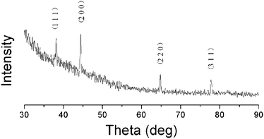 | ||
| Fig. 1 X-Ray diffraction pattern for the PI(6FDA/ODA)/silver nanohybrid film with a silver content of 0.067 wt%. | ||
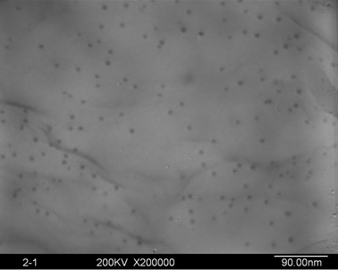 | ||
| Fig. 2 TEM image of the silver NPs in the hybrid films (silver content: 0.067 wt%). | ||
The current–voltage (I–V) characteristics of the sandwiched device using the PI/silver nanohybrid as the active layer were shown in Fig. 3a. In the first voltage scan from 0 V to −1.5 V, an abrupt increase in current was observed at a switching threshold voltage of about −0.8 V. The device jumps to a high conductivity state (ON state) from the low conductivity state (OFF state), which corresponds to the “writing” process for a memory device. Moreover, the device maintains its ON state during the subsequent second sweep from 0 to −1.5 V and does not relax to the OFF state after removal of the applied voltage. As the voltage sweeps from 0 to 3 V, a decrease in current is observed at a threshold voltage of about 2.5 V, corresponding to the “erasing” process for the memory device. The forth line shows that the memory device can maintain its OFF state after the device was turned off. The distinct bi-electrical states observed in the ranges of 0 to −0.8 V and 0 to 2.5 V allow a voltage such as 1 V to be used to “read” the information stored in the sandwiched memory device by simply identifying the ON state and OFF state current. In addition, voltage scans from the 5th sweep to the 8th sweep suggested that the device could be further written or erased when the switching threshold voltages were reapplied, indicating that the memory device is rewritable. Based on the analysis above, it can be concluded that a nonvolatile flash memory effect has been achieved in the current system.
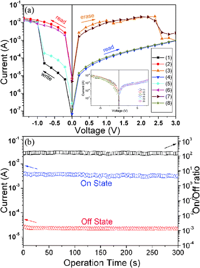 | ||
| Fig. 3 (a) I–V characteristics of the ITO|PI(6FDA/ODA)/silver nanohybrid film (silver content: 0.067 wt%)|Au device; (b) effect of the operation time (at 1 V) on the device current in the ON and OFF states and the ON/OFF current ratio vs. operation time; the inset in part (a) shows the I–V characteristic of a similar reference device but without silver NPs. | ||
I–V measurements on the sandwiched devices using a pristine 6FDA/ODA PI thin film as the active layer do not exhibit any special electrical characteristics, as shown as an inset in Fig. 3(a), implying that silver NPs in the system play a key role in the realization of the electrical bistability. Besides, it should be noted in Fig. 3(a) that the switching on voltage (−0.8 V) for the sandwich device is rather lower than the switching off voltage (2.5 V), implying that the current ITO|PI(6FDA/ODA)/silver nanohybrid film|Au device is easier in information “writing” than “erasing”. This is unusual and distinctive but not unexpected. Since the 6FDA moieties in the PI matrix possess excellent electron-withdrawing ability, it is reasonable to suggest that during the device switching on (“writing”) process, they greatly favor the injection of electrons into the silver NPs and the subsequent tunneling between them, therefore resulting in the occurrence of information “writing” at relatively low bias. Whereas, during the switching off (“erasing”) process, the electron-withdrawing nature of the 6FDA species in the PI matrix will significantly limit the charge release from the silver NPs and consequently leads to the shift of the “erasing” voltage to a higher level.
Fig. 3(b) shows the stability of the device and the ON/OFF current ratio as a function of operation time. The ability of the PI (6FDA/ODA)/silver nanohybrid material to retain the two states was tested under a constant stress of 1 V. As observed, no significant degradation of the device in both the ON and OFF states was observed during the measurement and the device maintained a stable ON/OFF current ratio at around 102.
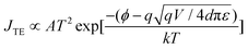
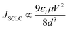
Several mechanisms are commonly proposed to explain the abrupt current transition in a dielectric film. They are Ohmic conduction, hopping conduction, Schottky emission, thermionic emission (TE), Frenkel–Poole emission, tunnel or field emission, direct tunneling, Fowler–Nordheim tunneling, ionic conduction and space-charge-limited current (SCLC) transport.1,4d,10,23 However, no single conduction mechanism can fit the characteristics of both the ON and OFF states. This indicates that there could be different charge transport mechanisms in a bistable cycle. We found the I–V characteristics at the OFF state are well fitted to the TE equation and the I–V characteristics at the ON state are well fitted to the SCLC model. The equations of the transport mechanisms for TE and SCLC are given by
 | (1) |
 | (2) |
As shown in Fig. 4a, a linear fitting behavior related to the TE process for the I–V curve is observed in the voltage range from 0 to −0.8 V, suggesting that the TE process probably dominates the charge transport for the device in the low-conducting state. However, the ln(I)–V1/2 curve can no longer be fitted to TE models after switching the device to the high-conducting state. Instead, the plot of log(I) versus log(V) exhibits very good linear relationship as shown in Fig. 4b, implying that the charge transport process of the device follows the SCLC model at the high-conducting state.
 | ||
| Fig. 4 (a) TE model for the device in the low-conducting state; (b) SCLC process for the device in the high-conducting state. | ||
3. Experimental section
3.1. Materials
6FDA (99%), isoquinoline (analytically pure) and 1,1,1-trifluoro-2,4-pentane-dione (98%, TFAH) were purchased from Alsa Aesar and used without further purification. 4,4′-ODA (99%) was purchased from Shanghai Research Institute of Synthetic Resins and used after recrystallization. m-Cresol (chemically pure; Sinopharm Chemical Reagent Co. Ltd) was distilled before use. Silver acetate (99%, AgAc) was purchased from Sinopharm Chemical Reagent Co., Ltd and dimethylacetamide (analytically pure, DMAc) was offered by Tianjin Guang Fu Fine Chemical Research Institute and used after distillation. Tetrahydrofuran (THF) and methanol were produced by Beijing Chemical Works and used as received. ITO glass was provided by Jintan Kangdake Optoelectronic Technology Co,. Ltd.3.2. Synthesis of 6FDA/ODA-based PI
To a solution of ODA (480 mg, 2.40 mmol) in m-cresol (15 ml) were added 6FDA (1065 mg, 2.40 mmol) and isoquinoline (750 μl). The mixture was stirred at 190 °C for 24 h under N2 environment. The 6FDA/ODA PI was obtained by pouring the reaction mixture into a large amount of methanol (500 ml) followed by decantation. The precipitate was then purified by re-dissolving in THF (10 ml) and re-precipitating in methanol (500 ml) twice. Finally, after being washed with methanol and dried at 60 °C under vacuum, a yellow powder was obtained (1384 mg, 90% yield). FTIR (KBr, cm−1) 1790, 1730, 1372 (imide); 1111 (–O–). 5 wt% thermal decomposition temperature (TGA): 533 °C. GPC analysis: Mn ≈ 95![[thin space (1/6-em)]](https://www.rsc.org/images/entities/char_2009.gif) 000, Mw/Mn ≈ 1.66. The synthetic procedure and chemical structure of the synthesized 6FDA/ODA PI was shown in Scheme 1.
000, Mw/Mn ≈ 1.66. The synthetic procedure and chemical structure of the synthesized 6FDA/ODA PI was shown in Scheme 1.
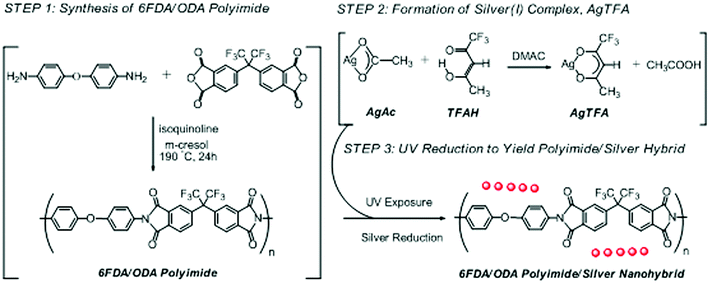 | ||
| Scheme 1 Illustrative protocol for the synthesis of 6FDA/ODA-based PI/silver nanohybrid films through in situ UV reduction. | ||
3.4. Characterization
Fourier transform infrared spectroscopy (FT-IR) spectra were recorded under ambient conditions on a Tensor 27 Fourier transform spectrometer (BRUKER, Germany). KBr was used as a nonabsorbent medium. A minimum of 32 scans with a resolution of 4 cm−1 was collected for each sample. Gel permeation chromatograph (GPC) analysis was carried out on a Waters 515–2410 system using THF as the eluent. X-Ray diffraction (XRD) data were collected on a D/Max2500VB2+/PC X-ray diffractometer (Rigaku, Japan) in the 5–90° range at a scanning rate of 0.18° per second. The X-ray beam was generated by a copper target (Cu-Kα, λ = 0.154 nm), using a working voltage of 40 kV and a current of 200 mA. Transmission electron microscope (TEM) images were recorded on a Hitachi H-800 TEM instrument. The current–voltage (I–V) measurements were carried out using a KEITHLEY-4200 semiconductor parameter analyzer. The thickness of the film was measured using atomic force microscopy (Digital Instruments Nanoscope IIIa, Veeco Instruments) under contact mode.3.5. Memory device fabrication
The sandwiched device, ITO|PI(6FDA/ODA)/silver nanohybrid film|Au, was fabricated and an illustrative structure of which was shown in Scheme 2. The ITO glass was precleaned sequentially with water, acetone, chloroform, and isopropanol in an ultrasonic bath for 15 min and then dried by an N2 gun.21 A PI/silver nanohybrid film (ca. 55 nm thick by AFM) was then deposited onto the ITO substrate by spreading the AgTFA-doped 6FDA/ODA PI solution (10 mg ml−1) using a spin coater at a rotating speed of 2000 RPM followed by exposure under UV for 20 min. Finally, 300 nm-thick Au top electrodes (cylinder shape with diameters of 4 mm, 3 mm, 2 mm and 1 mm) were plated onto the PI layer through a shadow mask.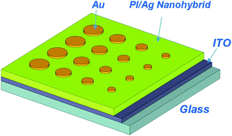 | ||
| Scheme 2 Illustrative structure for the sandwich device. | ||
4. Conclusion
As a summary, a functional PI (6FDA/ODA)/silver nanohybrid material has been synthesized in our present work. Semiconductor parameter analysis on the sandwiched ITO|PI (6FDA/ODA)/silver nanohybrid film|Au device suggests that the material possesses a nonvolatile electrical switching ability, endowing the device with readable, writable, retainable, erasable and re-writable functions, which are typical characteristics of the flash memory effect. Meanwhile, the device exhibits a low switching voltage (ca. −0.8 V), reading voltage (any voltage from 0 V to 2.5 V or 0 V to −0.8 V) and erasing voltage (ca. 2.5 V) and a stable ON/OFF current ratio at around 102. Experimental results suggest that the realization of electrical memory characteristics in our present system is strongly related to the presence of silver NPs. To the best of our knowledge, this is the first case for the realization of an electrical memory effect in a PI/metal based material. Although the ON/OFF current ratio in the present system is not so satisfactory, the current research pioneers work on the exploration of a class of low-cost, easily processable materials with the potential for future high-density data storage applications.Acknowledgements
This work was supported by the Program for Changjiang Scholars and Innovative Research Team in University (PCSIRT, IRT0706), Polymer Chemistry and Physics, Beijing Municipal Education Commission (BMEC, No. XK100100640), the National Natural Science Foundation of China (Project No. 50903006). And we are very grateful for the support of Professor Wenping Hu from the Institute of Chemistry, Chinese Academy of Sciences.References
- Q. D. Ling, D. J. Liaw, C. Zhu, D. S. H. Chan, E. T. Kang and K. G. Neoh, Prog. Polym. Sci., 2008, 33, 917 CrossRef CAS
.
-
(a) H. Gruber, Research Policy, 2000, 29, 725 CrossRef
-
(a) S. H. Cho, D. I. Lee, J. H. Jung and T. W. Kim, Nanotechnology, 2009, 20, 345204 CrossRef
-
(a) L. D. Bozano, B. W. Kean, M. Beinhoff, K. R. Carter, P. M. Rice and J. C. Scott, Adv. Funct. Mater., 2005, 15, 1933 CrossRef CAS
- L. Balan, J. P. Malval, R. Schneider and D. Burget, Mater. Chem. Phys., 2007, 104, 417 CrossRef CAS
-
(a) R. J. Tseng, J. Huang, J. Ouyang and R. B. Kaner, Nano Lett., 2005, 5, 1077 CrossRef CAS
-
(a) Z. Wu, D. Wu, S. Qi, T. Zhang and R. Jin, Thin Solid Films, 2005, 493, 179 CrossRef CAS
-
(a) S. Qi, Z. Wu, D. Wu and R. Jin, J. Phys. Chem. B, 2008, 112, 5575 CrossRef CAS
-
(a) K. Akamatsu, S. Ikeda and H. Nawafune, Langmuir, 2003, 19, 10366 CrossRef CAS
- H. T. Lin, Z. Pei and Y. J. Chan, IEEE Electron Device Lett., 2007, 28, 569 CrossRef CAS
- G. M. Porta, J. D. Rancourt and L. T. Taylor, Chem. Mater., 1989, 1, 269 CrossRef CAS
- Y. S. Hsiao, C. P. Chen, C. H. Chao and W. T. Whang, Org. Electron., 2009, 10, 551 CrossRef CAS
- T. Shimotori, E. E. Nuxoll, E. L. Cussler and W. A. Arnold, Environ. Sci. Technol., 2004, 38, 2264 CrossRef CAS
- S. Yoda, A. Hasegawa, H. Suda, Y. Uchimaru, K. Haraya, T. Tsuji and K. Otake, Chem. Mater., 2004, 16, 2363 CrossRef CAS
- B. L. French, L. M. Davis, E. S. Munzinger, J. W. J. Slavin, P. C. Christy, D. W. Thompson and R. E. Southward, Chem. Mater., 2005, 17, 2091 CrossRef CAS
- S. H. Xie, B. K. Zhu, X. Z. Wei, Z. K. Xu and Y. Y. Xu, Composites, Part A, 2005, 36, 1152 CrossRef
- Y. C. Yang, F. Pan, Q. Liu, M. Liu and F. Zeng, Nano Lett., 2009, 9, 1636 CrossRef CAS
- J. Zhan, Z. Wu, S. Qi, D. Wu and W. Yang, Thin Solid Films, 2011, 519, 1960 CrossRef CAS
- S. l. Köytepe and T. Seçkin, Ind. Eng. Chem. Res., 2008, 47, 4123 CrossRef
- S. Qi, Z. Wu, D. Wu, W. Wang and R. Jin, Langmuir, 2007, 23, 4878 CrossRef CAS
- Q. D. Ling, F. C. Chang, Y. Song, C. X. Zhu, D. J. Liaw, D. S. H. Chan, E. T. Kang and K. G. Neoh, J. Am. Chem. Soc., 2006, 128, 8732 CrossRef CAS
- L. Chen, Y. Shen, A. Xie, F. Huang, W. Zhang and S. Liu, Cryst. Growth Des., 2010, 10, 2073 CAS
-
(a) P. Y. Lai and J. S. Chen, Org. Electron., 2009, 10, 1590 CrossRef CAS
- S. L. Qi, W. C. Wang, D. Z. Wu, Z. P. Wu and R. G. Jin, Eur. Polym. J., 2006, 42, 2023 CrossRef CAS
| This journal is © The Royal Society of Chemistry 2012 |