Single-phase tungsten carbide nanopillar arrays prepared by chemical vapor deposition
Feng
Teng
,
Jiangtao
Wang
,
Xiuyun
An
,
Bingan
Lu
,
Yurong
Su
,
Chengshi
Gong
,
Peng
Zhang
,
Zhenxing
Zhang
and
Erqing
Xie
*
School of Physical Science and Technology, Lanzhou University, Lanzhou 730000, People's Republic of China. E-mail: xieeq@lzu.edu.cn; Fax: + 86 9318913554; Tel: +86 9318912616
First published on 26th July 2012
Abstract
Single-phase tungsten carbide nanopillar arrays have been prepared by hot filament chemical vapor deposition with carbonized tungsten filaments as precursors. The structural properties and morphologies of the nanopillar arrays were characterized by XRD, SEM and HRTEM, respectively. A possible formation mechanism for the morphology was proposed. Moreover, the field emission properties of the nanopillar arrays have been studied. The Fowler–Nordheim plot of the nanopillar arrays shows an interesting linear dependence demonstrating their suitability as emitters. The nanopillar arrays show remarkable stability for several hours at a current intensity of about 5.6 × 10⁻⁷ A at 2000 V with a distance between the anode and sample of 150 μm.
Tungsten carbide (WC) is one of the most important materials in both industry and high-pressure research due to its high melting temperature (2870 °C), hardness (16–22 GPa, 500 g load, Vickers), relatively low electrical resistivity (∼2 × 10⁻⁷ Ohm m), oxidation resistance, and excellent chemical stability.1 Owing to its excellent properties, WC has many applications such as field emitters in flat panel displays, cutting tools and abrasives in industrial machinery, anvil materials in multianvil high pressure instruments and seats in diamond anvil cells.2 There are many methods to synthesize WC, such as sputtering,3 solid-state synthesis,4 impregnation–compaction route,5 chemical vapor deposition (CVD) and so on. Among them, CVD has many advantages such as a versatile process, low maintenance, high purity, high yields, well controlled film properties and so on. Generally, in the CVD of tungsten carbide, metal halides (like hexafluoride and hexachloride) are the most common tungsten precursors while various hydrocarbons (acetylene, methane, ethylene, propane, etc.) provide the carbon source.6 However, the most common products are films.
There are many groups who have used tungsten carbide as an electrocatalyst because of its platinum-like catalytic behavior and stability in acidic and alkaline solutions.7–10 However, the electrocatalytic activity of the tungsten carbide was usually low. Decreasing the WC particle size further is, thereby, important in the investigation of non-noble electrocatalysts. Microwave-synthesized WC has a particle size <100 nm.11 Ganesan and Lee12 reported the synthesis of W2C microspheres with high surface areas and chemisorption capacity. This material when combined with platinum showed a very high activity for the electrooxidation of methanol exceeding that of a commercial Pt–Ru catalyst with a higher metal loading. High surface area plays an important role in the effect of catalysts. Therefore, nanostructured crystallized tungsten carbide is bound to lead to a new storm in its industrial applications.
In this report, single-phase WC nanopillar arrays have been synthesized by hot filament chemical vapour deposition (HFCVD). The formation mechanism of the morphology and the field emission properties of the nanopillar arrays were investigated.
The detailed steps of the experiment are as follows. Firstly, a tungsten filament of length 16 cm and diameter 0.6 mm was coiled into nine turns. Secondly, the silicon substrates were ultrasonically cleaned in acetone and alcohol each for 10 min and then placed under the filament. Thirdly, the chamber was pumped down to 1.0 × 10⁻³ Pa. Fourthly, the filament was carbonized at 2000 °C for 3 h in a CH4–H2 gas mixture with a volumetric ratio of 0.035 and a total flow rate of 200 standard cubic centimetres per minute (SCCM). This process makes sure that the filament is stable and supplies a precursor for the next WC growth. Finally, the WC nanopillar arrays were prepared in a hydrogen atmosphere with a flow rate of 40 SCCM and a pressure below 1000 Pa at a filament temperature of 2000 °C.
The surface morphologies and structure properties of the sample were characterized by scanning electron microscopy (SEM, Hitachi S-4800), high resolution transmission electron microscopy (HR-TEM, FEI Tecnai G2 F30) and a X-ray diffraction analyzer (XRD, PANalytical X'Pert). The field electron emission measurements were performed under a base pressure of 1.4 × 10⁻³ Pa with a distance of 150 μm between the anode and the sample. A picoammeter with a power supply (Keithley 6487) was employed for the tests.
Fig. 1(a) shows a low resolution SEM image of the sample. Obviously, the sample shows a columnar structure, and the adjacent pillars separate from the root. The obvious edges and corners of the pillar can be observed in Fig. 1(b). The inset is the corresponding HR-TEM image. The diameters of the pillar are estimated to be tens to hundreds of nanometres in our experiment. The structure marked by a red circle in Fig. 1(b) is of the perfect configuration for an electron emitter. The main factor may be the low carbon content in the WC crystal. Shi et al.13 reported that when C diffused into the tungsten filament, both WC and graphite were converted to W2C. It revealed that W2C was the main product during the carbonization procedure with the tungsten filament at high temperature. The pillar fabricated by carbonized tungsten consisted of W2C and WC with lower carbon content, which can be verified from Fig. 2. The two XRD peaks marked with SiO2 are originally from the substrate. The other XRD peaks are related to WC. The XRD patterns indicate that the crystalline structure of WC exhibits hexagonal α-WC and hcp α-W2C structures.14,15 Though Yang et al.16 mentioned the crystalline WC dominated the sample's structure, excess carbon atoms might adhere to the surface of the WC grain and form amorphous carbon in WC. Therefore, the sharpness of the tip formed by WC would be reduced or even destroyed by the amorphous carbon. That may be the reason why the main products are WC films while the hydrocarbon provides the carbon source. Generally, a low carbon content in WC promotes the formation of nanopillar arrays.
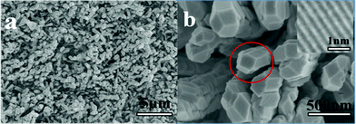 | ||
| Fig. 1 (a) The low resolution SEM image of the sample. (b) The local amplified image of the sample. Inset: corresponding HR-TEM image. | ||
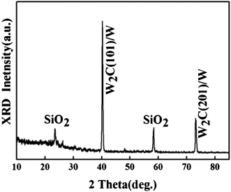 | ||
| Fig. 2 XRD patterns of the single-phase WC nanopillar arrays. | ||
To study the field emission properties of the nanopillar arrays, we used a conventional field emission measurement method as follows: the sample was placed on a sample holder that was connected to a cathode while the anode was placed 150 μm over the sample.
Here, we define the turn-on field (Eto) as the electric field required to produce a current density of 1 μA cm−2. The Eto for WC nanopillars was 12 V μm−1. This value was lower than that of SnO2 nanoneedles17 and thin multiwalled carbon nanotubes (thin-MWCNTs).18 The reason for the high turn-on electric field is probably due to the low density of the nanopillar. We applied a voltage bias between the anode and the sample, and simultaneously measured the current with a sensitivity of the order of 10 nA. To analyze the field emission characteristics, we refer to the Fowler–Nordheim (FN) theory,19 which relates the emission current density J to the electric field (E) at the emitter surface and to the work function (ϕ) of the material, as expressed by the eqn (1)
| J = (Aβ2E2/ϕ)exp(−Bϕ3/2/βE) | (1) |
| K = −Bϕ3/2/β | (2) |
Fig. 3(b) shows the FN plot of the I–V curve of Fig. 3(a). The slopes of the FN plots for the sample are −9.867 and −11.056, and the average field enhancement factor can be extrapolated as 4473 using the work function of ϕ = 3.6 eV for WC.20 Compared with the needle-shaped SnO2 nanostructures mentioned above, it is high enough for various applications of field emission. The other important factor of the WC nanopillar arrays is their emission stability. Applying a constant voltage, emission current versus time I(t) was measured in order to verify the stability. Fig. 4 shows a 200 min segment of the stability at a constant voltage of 2000 V with a distance of 150 μm. The current shows a good stability at 5.6 × 10⁻⁷ A with a less than 0.1% root mean square fluctuation. From the figure, the stability of the WC nanopillar arrays is considerable.
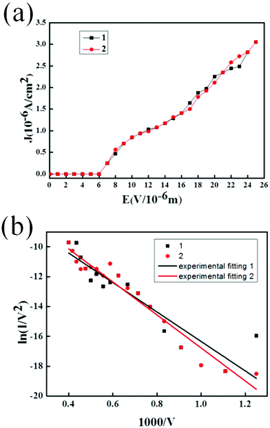 | ||
| Fig. 3 (a) The field emission properties of the sample at a distance of 150 μm (the same sample measured twice) and (b) the corresponding FN plot and the fitting curve. | ||
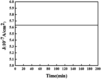 | ||
| Fig. 4 Field emission current stability of the sample measured by applying a fixed bias of 2000 V. | ||
Conclusions
Single-phase WC nanopillar arrays were prepared by HFCVD. Amorphous carbon may be formed by excess carbon in WC and the morphology of the nanopillar is destroyed. XRD patterns show that pillars fabricated by carbonized tungsten consist of W2C and WC with lower carbon content. The field emission (FE) feature was well described by standard FN theory, and the field emission current was extremely stable over a period of about 200 min with a current intensity about 5.6 × 10⁻⁷ A at 2000 V and a distance of 150 μm between the anode and the sample. Our study shows that single-phase WC nanopillar arrays have large field enhancement factors and excellent stability.Acknowledgements
This project was supported by the National Natural Science Foundation of China (No. 61176058) and partially supported by the Fundamental Research Funds for the Central Universities of China (NO. lzujbky-2010-82).References
- R. Koc and S. K. Kodambaka, J. Eur. Ceram. Soc., 2000, 20, 1859–69 CrossRef CAS.
- Z. J. Lin, L. Wang, J. Z. Zhang, H. K. Mao and Y. S. Zhao, Appl. Phys. Lett., 2009, 95(211906), 1–3 Search PubMed.
- H. Romanus, V. Cimalla, J. A. Schaefer, L. Spiess, G. Ecke and J. Pezoldt, Thin Solid Films, 2000, 359, 146–9 CrossRef CAS.
- E. J. Rees, C. D. A. Brady and G. T. Burstein, Mater. Lett., 2008, 62, 1–3 CrossRef CAS.
- X. Z. Cui, H. Li, L. M. Guo, D. N. He, H. R. Che and J. L. Shi, Dalton Trans., 2008, 6435–40 RSC.
- K. A. Beadle, R. Gupta, A. Mathew, J. G. Chen and B. G. Willis, Thin Solid Films, 2008, 516, 3847–54 CrossRef CAS.
- C. J. Barnett, G. T. Burstein, A. R. J. Kucernak and K. R. Williams, Electrochim. Acta, 1997, 42, 2381–8 CrossRef CAS.
- S. Bodoardo, M. Maja, N. Penazzi and F. E. G. Henn, Electrochim. Acta, 1997, 42, 2603–9 CrossRef CAS.
- M. B. Zellner and J. G. Chen, Catal. Today, 2005, 99, 299–307 CrossRef CAS.
- H. J. Zheng, J. G. Huang, W. Wang and C. A. Ma, Electrochem. Commun., 2005, 7, 1045–9 CrossRef CAS.
- E. J. Rees, K. Essaki, C. D. A. Brady and G. T. Burstein, J. Power Sources, 2009, 188, 75–81 CrossRef CAS.
- R. Ganesan and J. S. Lee, Angew. Chem., Int. Ed., 2005, 44, 6557–60 CrossRef CAS.
- Y. J. Shi, L. Tong, B. D. Eustergerling and X. M. Li, Thin Solid Films, 2011, 519, 4442–6 CrossRef CAS.
- A. A. Voevodin, J. P. O'Neill, S. V. Prasad and J. S. Zabinski, J. Vac. Sci. Technol., A, 1999, 17(3), 986–92 CAS.
- P. D. Rack, J. J. Peterson, J. Li, A. C. Geiculescu and H. J. Rack, J. Vac. Sci. Technol., A, 2001, 19(1), 62–5 CAS.
- B. Q. Yang, X. P. Wang, H. X. Zhang, Z. B. Wang and P. X. Feng, Mater. Lett., 2008, 62, 1547–50 CrossRef CAS.
- L. A. Ma and T. L. Guo, Mater. Lett., 2009, 63, 295–7 CrossRef CAS.
- G. H. Chen, D. H. Shin, S. Kim, S. Roth and C. J. Lee, Nanotechnology, 2010, 21(015704), 1–6 Search PubMed.
- R. H. Fowler and L. Nordheim, Proc. R. Soc. London, Ser. A, 1928, 119, 173–81 CrossRef CAS.
- M. L. Yu, B. W. Hussey, E. Kratschmer and T. H. P. Chang, J. Vac. Sci. Technol., B, 1995, 13(6), 2436–40 Search PubMed.
| This journal is © The Royal Society of Chemistry 2012 |