Hybrid single/poly-crystalline ZnO nanoawl arrays: facile synthesis and enhanced field emission properties†
Feng
Xu‡
a,
Jing
Chen‡
b,
Yunsong
Di
bc,
Yunkang
Cui
b,
Jun
Sun
a,
Litao
Sun
*a,
Wei
Lei
b,
Chunxiang
Xu
d and
Weilie
Zhou
*e
aSEU-FEI Nano-Pico Center, Key Laboratory of MEMS of Ministry of Education, Southeast University, Nanjing, 210096, China. E-mail: slt@seu.edu.cn; Fax: +86-25-83792939; Tel: +86-25-83792632 ext. 8813
bJiangsu Information Display Engineering Research Center, School of Electronic Science and Engineering, Southeast University, Nanjing, 210096, China
cSchool of Physics and Technology, Nanjing Normal University, Nanjing, 210046, China
dSchool of Biological Science & Medical Engineering, Southeast University, Nanjing, 210096, China
eAdvanced Materials Research Institute, University of New Orleans, New Orleans, LA 70148, USA. E-mail: wzhou@uno.edu
First published on 20th September 2012
Abstract
Arrays of hybrid single/poly-crystalline ZnO nanoawls (HSP-ZNAs) composed of single-crystalline ZnO nanorod (ZNR) holders and poly-crystalline nanoneedles were for the first time fabricated via a facile two-step synthesis strategy that was based on firstly an aqueous electrodeposition and secondly an aqueous chemical growth (ACG). The two-step synthesis strategy not only can ensure reliable electrical contact between the ZNR holders and the substrates, but also can afford control over the crystal structure and aspect ratio of the nanoneedles. The as-grown HSP-ZNA arrays exhibited markedly enhanced field emission (FE) current at lower electric fields compared with the whole single-crystalline ZNA arrays or ZNR arrays without nanoneedles. The improvement could be attributed to more emission sites from the tips of poly-crystalline nanoneedles of the HSP-ZNAs. Our results demonstrate the HSP-ZNA arrays one of the promising candidates for FE devices, and also provide a new paradigm for synthesizing novel hybrid single/poly-crystalline nanostructures that could find many potential applications in electronics and optoelectronics.
1. Introduction
Arrays of one-dimensional (1D) nanostructures with high aspect ratios, including CNTs,1,2 W nanowires,3 SiC nanowires,4 ZnO nanorods,5 MoO3 nanobelts,6 AlN nanotubes,7 and SnO2 nanorods,8 are considered to be promising field emitters that can emit electrons at low electric fields. Among these, ZnO-based 1D nanostructures have attracted much attention and are appropriate alternatives to CNTs for field-emission (FE) devices due to their high mechanical strength, thermal stability, oxidation resistibility, negative electron affinity, and ideal geometry of high aspect ratio.9 It is demonstrated that electrons are more easily emitted from ZnO nanostructures with sharp tips or surface perturbations than from nanowires with uniform diameter.10 Therefore, much effort has been devoted to developing various approaches to fabricate 1D ZnO nanoneedles,10,11 nanopencils,12 nanopins,13 and nanoinjectors,14,15 nanonails16 that have characteristically sharp tips.For instance, the vapor-phase transport method was utilized to grow ZnO nanopencils, nanopins, and nanoinjectors.12–15 Metalorganic chemical vapor deposition (MOCVD) was also used to fabricate well-aligned ZnO nanoneedle arrays.9 Although these techniques can easily get high-quality products, they are generally constrained by the requirement of high temperature and substrates that must be able to endure high temperature, which limits large-scale production with low energy consumption on other substrates.
In contrast, mild solution-based synthesis methods offer economically viable alternative synthesis routes for the aforementioned 1D ZnO nanostructures.17 For instance, A. Wei et al.18 fabricated ZnO nanoinjectors by chemical dissolution of hydrothermaly grown ZnO nanorods. However, so far all existing synthesis methods can only obtain 1D arrays of single-crystalline ZnO nanostructures with a single sharp tip as an electron emission site, which limits the FE current at a low level. Increasing the area density of 1D ZnO nanostructures to obtain more electron emission sites also cannot improve the FE performance all the time due to the concomitant serious screening effect.14 Thus, further increasing the number of FE sites by tuning the tips' crystal structure and surface perturbations without increasing the screening effect will be a meaningful and challenging attempt.
In this paper, we designed a facile two-step synthesis strategy to create 1D arrays of novel hybrid single/poly-crystalline ZnO nanoawls (HSP-ZNAs). Each HSP-ZNA consists of a poly-crystalline ZnO nanoneedle atop a single-crystalline ZnO nanorod (ZNR). The poly-crystalline nanoneedle was made up of tiny nanocrystallites several nanometers in size and could provide more surface perturbations and thus more electron emission sites, which will help field emitters improve their FE properties. To the best of our knowledge, this is the first example of successfully fabricating 1D HSP ZnO nanostructures. It is demonstrated that the HSP-ZNA arrays exhibited markedly enhanced FE properties compared with whole single-crystalline ZNA arrays or the ZNR arrays without nanoneedles. So far, there have been no reports on the enhancement of FE properties by incorporating poly-crystalline ZnO nanostructures into pristine single-crystalline ZnO nanostructures. In addition, our two-step approach is based firstly on an aqueous electrodeposition and secondly, aqueous chemical growth (ACG) can afford a tunable crystal structure and aspect ratio of the ZNAs. In addition, the two-step synthesis strategy could possibly be extended to the fabrication of HSP nanostructures of other functional materials.
2. Experimental section
The HSP-ZNA arrays were produced on a large scale via a facile two-step synthesis strategy similar to our previous reports.19,20 Typically, in the first step, large-scale ZNR arrays were electrodeposited on indium tin oxide (ITO, In![[thin space (1/6-em)]](https://www.rsc.org/images/entities/char_2009.gif) :SnO2) glass substrates (10 Ω/□) in an equimolar concentration (0.005 M) aqueous solution of Zn(NO3)2 and C6H12N4 (HMT) using a CHI-660D electrochemical workstation with a three-electrode electrochemical configuration (see Fig. 1a) that can be found elsewhere.21 In brief, an ITO substrate, a Pt electrode, and a saturated calomel electrode (SCE) were used as the working electrode, the counter electrode, and reference electrode, respectively. The applied potential and temperature was kept at −1.1 V and 70 °C, respectively. In the second step, an aqueous chemical growth (ACG) method22 (see Fig. 1b) was adopted to grow ZnO nanoneedles on the hexagonal end plane of the ZNRs by immersing the ZNRs' substrate obtained from the first step into the bottle filled with an aqueous solution consisting of Zn(NO3)2, C6H12N4, and NaF. The bottle was sealed and kept at a constant temperature of 90 °C. The molar concentration and ratio of Zn(NO3)2, C6H12N4, and NaF were tuned to obtain single-crystalline or poly-crystalline nanoneedles. Finally, the as-synthesized product on ITO substrates were annealed at 450 °C in vacuum and then used for further characterization and FE measurement.
:SnO2) glass substrates (10 Ω/□) in an equimolar concentration (0.005 M) aqueous solution of Zn(NO3)2 and C6H12N4 (HMT) using a CHI-660D electrochemical workstation with a three-electrode electrochemical configuration (see Fig. 1a) that can be found elsewhere.21 In brief, an ITO substrate, a Pt electrode, and a saturated calomel electrode (SCE) were used as the working electrode, the counter electrode, and reference electrode, respectively. The applied potential and temperature was kept at −1.1 V and 70 °C, respectively. In the second step, an aqueous chemical growth (ACG) method22 (see Fig. 1b) was adopted to grow ZnO nanoneedles on the hexagonal end plane of the ZNRs by immersing the ZNRs' substrate obtained from the first step into the bottle filled with an aqueous solution consisting of Zn(NO3)2, C6H12N4, and NaF. The bottle was sealed and kept at a constant temperature of 90 °C. The molar concentration and ratio of Zn(NO3)2, C6H12N4, and NaF were tuned to obtain single-crystalline or poly-crystalline nanoneedles. Finally, the as-synthesized product on ITO substrates were annealed at 450 °C in vacuum and then used for further characterization and FE measurement.
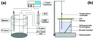 | ||
| Fig. 1 Schematic diagrams of experimental devices for (a) aqueous electrodeposition and (b) aqueous chemical growth methods. | ||
The surface morphology and phase identification of the samples were investigated by a scanning electron microscope (SEM, JSM-5900, JEOL, Japan) operated at an acceleration voltage of 15 kV and a powder X-ray diffractometer (XRD, ARL XTRA, Thermo Electron Co., USA) with Cu-KαB radiation at a scan speed of 5°/min in the 2θ range between 20° and 65°. The tube voltage and the tube current were 45 kV and 35 mA, respectively. Further structural analysis of the samples was carried out using a transmission electron microscope (TEM, Tecnai G20, FEI, USA) having a point-to-point resolution of 0.24 nm and a line resolution of 0.14 nm operated at an acceleration voltage of 300 kV. The TEM was equipped with a multiscan charge-coupled device (CCD) camera system (Model 8322, Gatan, USA) to record the HRTEM images and selected area electron diffraction (SAED) patterns. The chemical composition of the as-synthesized samples was analyzed using an energy dispersive X-ray spectrometer (EDS, EDAX Inc., USA). The FE measurement was performed with a simple diode configuration (see Fig. 2) in a bell jar which was pumped down to 10−6 Torr at room temperature. The cathode was the as-prepared hybrid single/poly-crystalline ZNA arrays on the ITO glass and the anode was ITO glass coated with a layer of fluorescent powder. The distance between the cathode and anode was 100 μm separated by a Teflon spacer with an aperture (∼0.5 cm2) for electron emission. The dependence of the emission current on the applied voltage was acquired at a step of 50 V. The data were recorded only after ramping up and down the applied voltage at least five times (electrical annealing) to stabilize the electron emission.
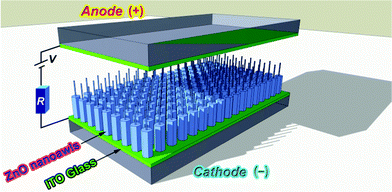 | ||
| Fig. 2 Schematic diagram of a simple diode configuration for measuring FE properties of ZnO nanoawl arrays. | ||
3. Results and discussion
SEM images of the as-electrodeposited ZNR arrays and the derivative ZNA arrays prepared by subsequent ACG process are shown in Fig. 3. An aqueous solution consisting of Zn(NO3)2, C6H12N4, and NaF with a molar concentration ratio of 1:1:3.5 was used in the ACG process and the molar concentration of Zn(NO3)2 was 0.01 M. From the top-view and cross-section SEM images in Fig. 3a and c, it can be seen that the hexagonal ZNRs with 150–200 nm in diameter were primarily oriented perpendicular to the ITO substrate. After a 1 h ACG process and an annealing treatment, the pristine ZNRs evolved into the hierarchical ZnO nanostructures composed of two parts: a long needle atop a hexagonal rod base, resembling an awl in appearance, as shown in Fig. 3b and d. Thus, we called it a ZnO nanoawl (ZNA). It can be observed that each ZNA only has a single nanoneedle atop the nanorod holder, which is similar to our previous reports dealing with vapour-phase synthesis methods.14,15 These nanoneedles are uniform and ∼30 nm in diameter, and their length is mainly dependent on the ACG time. The longer the ACG time was, the larger the aspect ratio of the nanoneedles was. It is worth pointing out that the nanorod holders still have the same length, diameter, and perpendicularity to the pristine ZNRs. The preparation procedure of the ZNA arrays derived from the electrodeposited ZNR arrays can be schematically illustrated in Fig. 4.
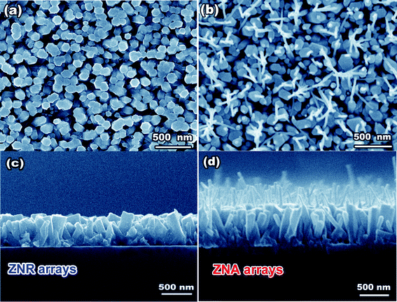 | ||
| Fig. 3 (a, b) Top-view and (d) cross-section SEM images of the ZNR arrays and ZNA arrays. | ||
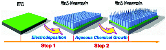 | ||
| Fig. 4 Schematic diagram of preparation procedure for the ZNA arrays via a facile two-step synthesis strategy based on an aqueous electrodeposition and an aqueous chemical growth. | ||
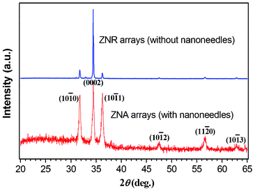
Fig. 5 shows the typical XRD patterns of the ZNR arrays and ZNA arrays, respectively. All diffraction peaks of both the two ZnO nanostructures can be indexed to the wurtzite (hexagonal) structured ZnO (space group P63mc) with cell parameters a = 3.249 Å and c = 5.206 Å, which is in good agreement with the literature values (JCPDS No.36-1451). No characteristic diffraction peaks of other impurities such as metallic Zn could be detected, indicating a pure ZnO phase. The XRD results prove the successful fabrication of the ZNA arrays. In addition, the strongest peak (0002) is observed implying that the (0002) plane of ZnO nanostructures was oriented parallel to the substrate. Compared with the ZNR arrays, the ZNA arrays have a lower diffraction peak intensity of the (0002) plane, which could be attributed to the crystal structure of the nanoneedles atop the ZNRs (the detailed reason will be mentioned below).
 | ||
| Fig. 5 Typical XRD patterns of the ZNR arrays and ZNA arrays, respectively. | ||
The crystal structure and morphology of the ZNAs were further investigated by TEM characterization. Fig. 6a shows the low-magnification TEM image of the ZNA arrays scraped from the ITO substrate, exhibiting the typical awl-like morphology. Further, from the high-resolution TEM (HRTEM) image of a nanoneedle tip in Fig. 6b, we can see that the nanoneedle consisted of randomly assembled ZnO nanocrystallites with less than 10 nm in size, indicating the poly-crystalline nature as revealed by the SAED pattern of annular diffraction ring inserted in Fig. 6b. The nanorod holders of the ZNAs kept the single-crystalline nature all the time, which also was proved by the HRTEM image and the SAED pattern of arrayed diffraction spots shown in Fig. 6c.
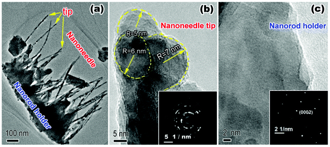 | ||
| Fig. 6 (a) Low-magnification TEM image of the ZNA arrays, (b) HRTEM image and SAED pattern of nanoneedle tip of the ZNAs, and (c) HRTEM image of nanorod holder of the ZNAs. | ||
The poly-crystalline nature of the ZnO nanoneedles could come from the intermediate product—poly-crystalline ZnFOH nanoneedles that were formed by the ACG process according to the previous reports.21,23 The EDS analysis (Fig. 7) also detected the presence of fluorine in the ZNAs before annealing as well as zinc and oxygen elements, corroborating the formation of ZnFOH. After the subsequent annealing treatment of ZnOHF nanoneedles, the poly-crystalline ZnO nanoneedles were formed at the top of single-crystalline ZNRs with the (0002) planes oriented parallel to the substrate. This explains the decrease in the (0002) diffraction peak intensity in XRD patterns for the ZNA arrays in Fig. 5. It is worth noting that this kind of poly-crystalline ZnO nanoneedle was not always obtained. When the NaF content in the ACG solution was decreased (molar concentration ratio Zn(NO3)2, C6H12N4, and NaF < 1:1:2), no intermediate product of ZnFOH was formed. On the contrary, single-crystalline ZnO nanoneedles were directly grown at the top of single-crystalline ZNRs (not shown), forming the whole single-crystalline ZNA arrays that have the nearly same morphology, size, and density as the HSP-ZNA arrays (see SEM and TEM images in Fig. S1 and S2 ESI†). This indicates that a critical molar concentration and ratio of Zn(NO3)2, C6H12N4, and NaF is the precondition at which ZnFOH can nucleate and grow.23 When it comes to this, we can safely proclaim that we have successfully fabricated the HSP-ZNA arrays. Therefore, the ACG process in the second step played a paramount role.
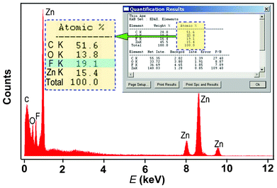
Fig. 8a shows the dependencies of the measured FE current density (J) on the applied electric field (E) in the J–E plots for the ZNR arrays, the single-crystalline ZNA arrays, and the HSP-ZNA arrays. For more impartial comparison, the single-crystalline ZNA arrays and the HSP-ZNA arrays have entirely the same size and morphology, the only difference being the crystal structure of the nanoneedles (see Fig. S1 and S2 ESI†). Apparently, the HSP-ZNA arrays have the lowest macroscopic turn-on field (defined as the electric filed required to draw a current density of 10 μA cm−2) of 1.7 V μm−1 and the lowest threshold field (defined as the electric filed required to draw a current density of 1 mA cm−2) of 4.7 V μm−1. In comparison, the turn-on and threshold fields of the single-crystalline ZNA arrays are 4.5 V μm−1 and 7.6 V μm−1, respectively. Unsurprisingly, the ZNR arrays didn't emit when the applied electric field was less than 10 V μm−1, which is attributed to a lack of nanoneedle emitters. Further, the FE current–voltage characteristics can be evaluated by the simplified Fowler–Nordheim (F–N) equation,24,25
| J = A(β2E2/Φ)exp(−BΦ3/2/βE) |
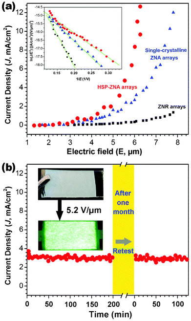 | ||
| Fig. 8 (a) FE current density as a function of applied electric field for the HSP-ZNA arrays, single-crystalline and ZNR arrays. The inset is the F–N plots; (b) Current density as a function of time recorded for the HSP-ZNA arrays at 5.2 V m−1, the insets are the photographs of the HSP-ZNA array sample and the corresponding fluorescent powder luminescence. | ||
Where J is the current density, E is the applied field strength, Φ is the work function of the emitter, which is 5.3 eV for ZnO, A and B are constants with values of A = 1.56 × 10⁻¹⁰ (A V−2 eV), B = 6.83 × 10⁹ (V eV−3/2 μm−1), respectively, and β is the so-called field enhancement factor that is introduced to reflect the degree of FE enhancement of any tip over a flat surface. The inset in Fig. 8a shows the F–N equation in the ln(J/E2) − 1/E plots for the three ZnO samples. All the plots exhibit quasi-linear dependence, indicating that the FEs from these samples follow the F–N relation. According to the slopes of fitting curves (as solid lines),24,25 the β was estimated to be 1946, 4507, and 6619 for the ZNR arrays, the single-crystalline ZNA arrays, and the HSP-ZNA arrays, respectively. Obviously, the HSP-ZNA arrays have the largest β value and the best FE performance according to Fig. 8a.
The value of nanostructured ZnO is related to the geometry, crystal structure, and nanostructure density.13 Because the single-crystalline ZNA arrays and the HSP-ZNA arrays have the entirely same size and morphology, the only difference being the crystal structure of the nanoneedles, we think that the increased β of the HSP-ZNA arrays was attributed to the poly-crystalline structure of ZnO nanoneedles atop the HSP-ZNAs, which increased the number of FE sites due to the presence of tiny ZnO nanocrystallites around the nanoneedle tips (see Fig. 6b). Moreover, the poly-crystalline ZnO has a lower work function compared with the single-crystalline ZnO,26 which made the poly-crystalline ZnO nanoneedle tips more easily emit electrons. As a result, the HSP-ZNA arrays have the lowest macroscopic turn-on field and threshold field. In other word, at the same electric field strength, the HSP-ZNA arrays could emit a larger FE current that is usually necessary for realizing high brightness FE displays and other FE-based devices. In addition, the FE lifetime and stability are also paramount issues in FE devices. We have conducted lifetime measurements at a pressure of 10−6 Torr with an initial emission current density of 3.0 mA cm−2 at 5.2 V μm−1. Fig. 8b shows the FE stability of the HSN-ZNA arrays by plotting the emission current density as a function of time. No obvious degradation of current density was observed during the period of 200 min FE. Even after one month, the same sample of the HSN-ZNA arrays was re-tested and still remained stale FE current density. The relatively stable FE is supposed to be related to the reliable contact between the ITO substrates and the ZNA arrays due to the direct electrodeposition on the substrates of ZNA holders. All these demonstrate that the HSN-ZNA arrays could be considered as one of the promising candidates for long-lifetime and high-stability FE devices.
4. Conclusions
In conclusion, we reported the fabrication of the HSN-ZNA arrays by a facile two-step synthesis strategy for the first time, and the formation mechanism of the novel 1D ZnO nanostructure was also proposed. The enhanced FE of the HSN-ZNA arrays was found and proposed to be related to more emission sites from the tips of poly-crystalline nanoneedles of the HSP-ZNAs. The proposal was further corroborated by an in situ transmission electron microscopy investigation of individual HSN-ZNAs during their FE process. In addition, our presented synthesis strategy could possibly be extended to the fabrication of HSP nanostructures of other functional materials that could have unexpected properties and potential applications.Acknowledgements
This work was supported by the National Basic Research Program of China (973 Program, Grant Nos. 2011CB707601 and 2009CB623702), the National Natural Science Foundation of China (NSFC, Grant Nos. 61106055 and 51071044), and Open Research Fund of State Key Laboratory of Bioelectronics.References
- A. Pandey, A. Prasad, J. P. Moscatello and Y. K. Yap, ACS Nano, 2010, 4, 6760–6766 CrossRef CAS.
- N. S. Liu, G. J. Fang, W. Zeng, H. Zhou, H. Long and X. Z. Zhao, J. Mater. Chem., 2012, 22, 3478–3484 RSC.
- Y. Baek, Y. Song and K. Yong, Adv. Mater., 2006, 18, 3105–3110 CrossRef CAS.
- Z. Li, W. Ren and A. L. Meng, Appl. Phys. Lett., 2010, 97, 263117 CrossRef.
- H. He, J. C. She, Y. F. Huang, S. Z. Deng and N. S. Xu, Nanoscale, 2012, 4, 2101–2108 RSC.
- Y. B. Li, Y. Bando, D. Golberg and K. Kurashima, Appl. Phys. Lett., 2002, 81, 5048–5050 CrossRef CAS.
- Y. J. Kim, J. H. Guo, Y. J. Hong, J. M. Jeon, M. Kim, C. L. Liu and G. C. Yi, Nanotechnology, 2010, 21, 055303 CrossRef.
- H. Huang, C. K. Lim, M. S. Tse, J. Guo and O. K. Tan, Nanoscale, 2012, 4, 1491–1496 RSC.
- C. J. Park, D. K. Choi, J. Yoo, G. C. Yi and C. J. Lee, Appl. Phys. Lett., 2007, 90, 083107 CrossRef.
- Y. B. Li, Y. Bando and D. Golberg, Appl. Phys. Lett., 2004, 84, 3603–3605 CrossRef CAS.
- S. Marathe, P. Koinkar, S. Ashtaputre, V. Sathe, M. A. More and S. K. Kulkarni, Thin Solid Films, 2010, 518, 3743–3747 CrossRef CAS.
- R. C. Wang, C. P. Liu, J. L. Huang, S. J. Chen, Y. K. Tseng and S. C. Kung, Appl. Phys. Lett., 2005, 87, 013110 CrossRef.
- C. X. Xu and X. W. Sun, Appl. Phys. Lett., 2003, 83, 3806–3808 CrossRef CAS.
- C. Li, Y. S. Di, W. Lei, Q. Yin, X. B. Zhang and Z. W. Zhao, J. Phys. Chem. C, 2008, 112, 13447–13449 CAS.
- C. Li, Y. Yang, X. W. Sun, W. Lei, X. B. Zhang, B. P. Wang, J. X. Wang, B. K. Tay, J. D. Ye, G. Q. Lo and D. L. Kwong, Nanotechnology, 2007, 18, 135604 CrossRef CAS.
- J. Y. Zhang, Q. F. Zhang, T. S. Deng and J. L. Wu, Appl. Phys. Lett., 2009, 95, 211107 CrossRef.
- H. W. Kang, J. Yeo, J. O. Hwang, S. Hong, P. Lee, S. Y. Han, J. H. Lee, Y. S. Rho, S. O. Kim, S. H. Ko and H. J. Sung, J. Phys. Chem. C, 2011, 115, 11435–11441 CAS.
- A. Wei, C. X. Xu, X. W. Sun, W. Huang and G. Q. Lo, J. Disp. Technol., 2008, 4, 9–12 CrossRef CAS.
- F. Xu, M. Dai, Y. N. Lu and L. T. Sun, J. Phys. Chem. C, 2010, 114, 2776–2782 CAS.
- F. Xu, Y. T. Shen, L. T. Sun, H. B. Zeng and Y. N. Lu, Nanoscale, 2011, 3, 5020–5025 RSC.
- F. Xu, Y. N. Lu, L. T. Sun and L. J. Zhi, Chem. Commun., 2010, 46, 3191–3193 RSC.
- F. Xu, Y. N. Lu, Y. Xie and Y. F. Liu, J. Phys. Chem. C, 2009, 113, 1052–1059 CAS.
- N. Saito, H. Haneda, W. S. Seo and K. Koumoto, Langmuir, 2001, 17, 1461–1469 CrossRef CAS.
- T. Y. Zhai, M. F. Ye, L. Li, X. S. Fang, M. Y. Liao, Y. F. Li, Y. S. Koide, Y. Bando and D. Golberg, Adv. Mater., 2010, 22, 4530–4533 CrossRef CAS.
- R. P. Sugavaneshwar, T. Nagao and K. K. Nanda, RSC Adv., 2012, 2, 2713–2716 RSC.
- S. Kikuchi, Y. Takahashi and T. Sakata, Appl. Opt., 1969, 8, 42–44 CrossRef.
Footnotes |
| † Electronic supplementary information (ESI) available: Some additional SEM and TEM images about size, morphology, and density of HSP-ZNA and pure ZNA arrays. |
| ‡ These authors contributed equally to this work. |
| This journal is © The Royal Society of Chemistry 2012 |