Optical detection of single nano-objects by transient absorption microscopy†
Shun Shang
Lo
,
Mary Sajini
Devadas
,
Todd A.
Major
and
Gregory V.
Hartland
*
Department of Chemistry and Biochemistry, University of Notre Dame, Notre Dame, IN 46556-5670, USA. E-mail: ghartlan@nd.edu
First published on 19th October 2012
Abstract
In recent years there has been considerable effort in developing ultra-sensitive imaging techniques based on absorption. This mini-review describes recent results from our laboratory on detecting single nano-objects using transient absorption microscopy. This technique is extremely flexible, allowing the detection of single semiconductor and metal nanostructures with high sensitivity. The goal of this review is to illustrate key points in implementing transient absorption microscopy for ultra-sensitive detection, as well as to discuss the advantages and disadvantages of this technique compared to other optical absorption based methods.
The detection of single entities has an important role in Analytical Chemistry, as highlighted by the recent themed issue in the Analyst.1 Traditionally optical detection of single nano-objects (nanoparticles or molecules) is achieved by recording emission from the object.2 However, emission experiments suffer from fluorescence intermittency (“blinking”) and photo-bleaching (for organic fluorophores), which degrade the quality of the data, and limit observation times. Both of these effects can be a problem for studies of long timescale biological processes.3 Emission measurements also require species with high fluorescence quantum yields,2,4,5 which limits the range of materials that can be examined. This has led researches to look for alternative techniques to detect and study single objects.
Because of their strong interaction with light, metal nanoparticles have attracted much interest in imaging applications.6,7 Single metal nanoparticles can be conveniently detected through scattering utilizing a dark-field microscope.8 However, the intensity of light scattered from an object is proportional to the square of its volume,9 which means that scattering methods are limited to particles larger than ca. 20 nm. This is significantly larger than the size of organic dyes and inorganic quantum-dots used for fluorescence imaging. In contrast to scattering, optical absorption simply scales as the volume of the particle,9 so that, in principle, absorption can be used to detect smaller objects.10–12 This is important for labeling applications, for example, where the size of the label should be minimized. This has led to the development of a variety of absorption based single particle detection schemes.10
One of the most widely used absorption based techniques in nanoscience is photothermal heterodyne imaging (PHI).13 In this technique heating from a pump laser beam produces a local change in the refractive index, which creates a thermal lens in the sample. This changes the propagation of a non-resonant probe, producing a signal at a far field detector.13–16 When implemented with high frequency modulation of the pump beam, PHI can be extremely sensitive – allowing the detection of single chromophores.17 In part this sensitivity arises because the probe is non-resonant, so that the probe power can be increased to high levels. For shot-noise-limited detection, this leads to an increase in signal-to-noise proportional to the square root of the probe power.18 Single nanoparticles can also be detected by direct absorption, either by modulating the particle position and recording the change in probe transmission with a lock-in amplifier,19,20 through interferometric detection,21,22 or by using a balanced detector.23,24 However, these techniques operate at low frequencies, which means they are more susceptible to noise. Despite this limitation, single molecule sensitivity has been demonstrated in balanced detector measurements.24
Ideally, an absorption-based method should have several attributes to be widely applicable. (i) The technique should be relatively insensitive to inhomogeneities in the substrate, which can scatter laser light. Scattering from the substrate is a significant problem in direct absorption measurements, and such schemes require careful sample preparation.23,24 (ii) The signal from a nano-object should not depend too much on the properties of the environment. For PHI the strongest signals are obtained for environments with small heat capacities and large temperature dependent refractive indices.18,25,26 For example, the thermal properties of water, which is an important solvent for many applications, are not well suited to PHI experiments.
An alternative absorption based technique for detecting single nano-objects is transient absorption microscopy.27–29 In these experiments a pump laser beam is used to resonantly excite a nanostructure. The probe then monitors the change in the absorbance of the object induced by pump laser excitation, which can include contributions from transient absorption, transient bleach and stimulated emission. This technique was first used to detect single metal nanoparticles,30,31 and was independently developed and applied to imaging in biological systems.32,33 Compared to PHI, the signal level in transient absorption microscopy is not sensitive to environment. Higher frequency modulation can also be used in transient absorption microscopy,30,34 which in principle leads to higher sensitivity. In PHI the modulation frequency is limited by thermal diffusion: high modulation frequencies reduce the size of the thermal lens, which reduces the PHI signal.14,15 In practice, modulations frequencies less than one MHz are used in PHI.14 However, a significant disadvantage of transient absorption microscopy compared to PHI is that the laser systems used are much more complex and expensive (vide infra). In this mini-review we describe how to implement these experiments, and give examples of imaging metal and semiconductor nanostructures. We end with a review of the different nanoparticle systems that have been studied to date, concentrating on experiments performed with diffraction limited spatial resolution.
Fig. 1(a) shows a diagram of the experimental scheme for transient absorption microscopy. These experiments require stable laser sources, and have been exclusively done with high repetition rate Ti:Sapphire laser systems to date. These lasers provide sub-200 fs, near-IR laser pulses at a typical repetition rate of around 80 MHz and nJ pulse energies. For experiments with metal nanostructures the system relaxes fast enough that the repetition rate of the laser is not an issue. However, semiconductors have excited state lifetimes that can exceed 10 ns, and in this case a pulse-picker should be used to reduce the repetition rate.35,36 In principle these experiments could also be performed with mode-locked fiber lasers. However, such systems are typically not tunable, which makes it difficult to study a wide variety of materials. For Ti:Sapphire lasers the fundamental can be tuned from 720 nm to 1000 nm, near-UV colors can be created by second-harmonic generation, and visible and near-IR light can be obtained from an optical parametric oscillator.
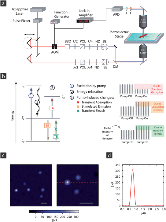 | ||
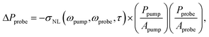
| Fig. 1 (a) Diagram of the experimental apparatus used for transient absorption microscopy. APD = avalanche photodiode; AOM = acousto-optic modulator; BE = beam expander; POL = polarizer; λ/2 and λ/4 = ½- and ¼-waveplates, respectively; ND = neutral density filter; DM = dichroic mirror. (b) Energy level diagram for the different photophysical process that can contribute to the transient absorption signal, see text for details. (c) Image of 20 nm Au nanoparticles. The images were taken with 720 nm pump and 530 nm probe pulses, with powers of 50 μW and 15 μW, respectively, at the sample. The scale bar in the images is 1 μm. (d) Line scan through the bright particle in the right panel of (c). The FWHM is 320 nm, close to the value expected for a diffraction limited spot at the probe wavelength. | ||
The output of the laser is split into two portions to create pump and probe beams. The relative timing between the pump and probe pulses is controlled by a translation stage, the two beams are combined with a dichroic mirror, and then focused at the sample with a high numerical aperture objective (for most experiments, objectives with NA >0.9 are used). For imaging experiments the pump and probe beams are spatially and temporally overlapped at the sample, and the change in transmission of the probe induced by the pump is detected. This is achieved by modulating the pump beam at high frequency with an acousto-optic modulator, and recording the beat note in the probe signal with a lock-in amplifier.
Typically different color pump and probe beams are used, allowing easy separation of the probe from the pump after the sample by optical filters. In experiments with molecules or semiconductors, the higher frequency beam is used as the pump and the lower frequency beam is used as the probe.35,36 In contrast, for metals near-IR light can be used to excite the nano-object.30,31,37Fig. 1(b) shows an energy level diagram for a transient absorption experiment on a semiconductor or molecular system. The pump laser populates an excited electronic state. This causes a bleach signal for transitions that originate from the ground electronic state, and stimulated emission and/or transient absorption signals for transitions involving the excited electronic state. The bleach and stimulated emission processes increase the transmission of the probe, whereas, transient absorption decreases the probe transmission. Note that a single-color, resonant four-wave mixing variant of transient absorption microscopy has recently been demonstrated on 40 nm gold particles.38 In these experiments the pump and probe beams were cross-polarized, and a polarizer was used to extinguish the pump after the sample.
Because high NA objectives are employed in these experiments, low pump and probe powers must be used to avoid damaging the sample. This means that high sensitivity, low noise-equivalent power (NEP) detectors are needed to monitor the probe.30 These measurements can be done in either transmission or reflection. However, when the probe is resonant to an absorption transition of the sample, transmission measurements are preferable, as they more efficiently collect light, allowing lower probe powers at the sample. Images are typically obtained by raster-scanning the sample through the laser focus with a piezo-stage, although these experiments can also be performed using galvo-mirrors to scan the beams across the sample,39 or by translating the objective with a piezo mount.40
Fig. 1(c) shows images of single gold nanoparticles from a sample with an average size of 20 nm. The images are presented as the signal-to-noise ratio, which was obtained by dividing the raw transient absorption images by the root-mean-square (rms) noise (determined from a region of the image where there are no particles). The experiments were performed with a modulation frequency of 1 MHz, a lock-in time constant of 30 ms with a pixel dwell time of 100 ms, and pump and probe powers of 50 μW and 15 μW at the sample, respectively. The differences in the signal-to-noise ratio for the different particles arise from differences in size and shape, which affect the amplitude and position of the plasmon resonance, respectively, of the particles.41 The brightest particles have a signal-to-noise ratio of greater than 300, which is comparable to what can be obtained from PHI.25,26 Note that these particles can hardly be seen in scattered light. These results imply that gold nanoparticles with diameters of a few nm could be detected with a signal-to-noise ratio of greater than 10 under these experimental conditions.
The limit of detection in these experiments is determined by the signal-to-noise (S/N) ratio, and in the following we give a brief derivation of this ratio. The signal in transient absorption experiments comes from the change in detected probe power ΔPprobe caused by pump laser induced modification of the absorption spectrum Δσabs of the sample. For transient absorption experiments on single particles, when the particle is much smaller than the laser spot size
| ΔPprobe = −Δσabs(ωpump,ωprobe,τ)Iprobe(x,y), | (1) |
| ΔPprobe = −σNL(ωpump,ωprobe,τ) × Ipump(x,y)Iprobe(x,y). | (2) |
When the nano-object is placed in the center of the focused pump and probe beams, the intensities in eqn (2) can be written as I = P/A where P is the power carried by the beam, and A = πw2/2 is the area of the equivalent top-hat beam.42 This gives
 | (3) |
The noise in these experiments arises from three sources: dark current from the detector (sdet = NEP), shot noise (sshot), and laser fluctuations (slaser). The total noise (stot) can be written as 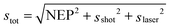 .43 The different contributions scale with laser power in different ways: the detector noise is independent of laser power,
  , and slaser ∝ P (both the pump and probe laser contribute to slaser). For our experiments (stable laser sources with Pprobe ≫ NEP), shot-noise is the dominant contribution to the noise. The shot noise contribution is given by
 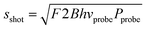 where F is the excess noise of the detector, and B is the bandwidth of the measurement.43 Combining the expression for sshot with eqn (3) yields the following expression for the signal-to-noise ratio (S/N):
 | (4) |
This equation is appropriate for nano-objects that are much smaller than the size of the pump and probe beams (i.e., particles). For nanowires, where the length of the object is much greater than the laser spot size, the signal has to be integrated over one dimension (see ESI†).44 In this case the signal-to-noise ratio can be written as:
 | (5) |
Eqn (4) and (5) show that there are a number of important factors in determining the signal-to-noise in these experiments. First, the maximum signal is obtained for high NA objectives, which create a small spot size at the sample.10,31 Second, in the shot-noise limit, increasing the power of either the pump or the probe improves the signal-to-noise. In practical applications, the power of the pump is limited by the damage threshold of the sample. For metal and semiconductor nanostructures with several hundred fs laser pulses, pump fluences less than a few tens of mJ cm−2 must be used.30,31 Note that the damage threshold depends on the laser pulsewidth: shorter pulses are very effective at ablating material45 and would require lower powers to avoid damaging the sample.
The situation is more complicated for the probe. In PHI, which employs a non-resonant probe beam, the power of the probe can be increased to high levels to increase the S/N ratio.18 However, in transient absorption experiments the probe is resonant to an optical transition of an object (which can be either a ground state bleach or an excited state absorption). For experiments with metal nanostructures, the probe is typically tuned to the plasmon resonance of the sample to maximize σNL(ωpump,ωprobe,τ). This means that there is significant absorption of the probe, which limits the power that can be used. For semiconductor nanostructures, transient absorption measurements can be performed with a near-IR probe, where there is no ground state absorption from the sample.35,36,46 The nonlinear optical transitions in this region are much weaker than the transitions near the band edge,47,48 so the power of the probe can be increased to improve the signal-to-noise without damaging the sample.
Fig. 2 shows images of a single CdSe nanowire recorded at different probe powers. These experiments were performed with pump and probe wavelengths of 400 nm and 800 nm, respectively, and a repetition rate of 5 MHz. The time constant for the measurement was 300 ms with a pixel dwell time of 1 s. The top panels in Fig. 2 show scattered light and fluorescence images of the nanowire, and an absorption cross-section measurement where each arm of the nanowire was scanned over the laser spot, and the change in transmission of the pump was recorded.36 The dip in this trace is related to the size and the absorption cross-section of the wire.49 These measurements show that the two arms of this nanowire are similar in size, which is consistent with the scattered light image. The middle set of panels show the raw transient absorption signal for different probe powers (measured at the sample), and the lower set of panels show the signal-to-noise ratio. The signal level in these experiments (∼8 μV) corresponds to a change in probe power of approximately 300 pW (calculated from the reported photosensitivity of our detector). This is much greater than the NEP of the detector (0.6 pW for a time constant of 300 ms).
 | ||
| Fig. 2 Top: scattered light image and fluorescence image of a branched CdSe nanowire. The panel on the right shows absorption cross-section measurements for the two arms of the nanowire. Middle: transient absorption images (7 × 7 μm2 image size) of the nanowire recorded with 1.5 μW pump power at the sample, and different probe laser powers. Bottom: signal-to-noise ratios for the transient absorption images. | ||
The signal-to-noise ratio in Fig. 2 increases with probe power up to 100 μW, at powers greater than this we start to saturate the detector, which reduces the fidelity of the image. The increase in signal-to-noise with probe power demonstrates shot-noise limited detection: if laser fluctuations were the dominant noise source, the signal-to-noise ratio would be independent of the probe power. The data shows that signal-to-noise levels of 120![[thin space (1/6-em)]](https://www.rsc.org/images/entities/char_2009.gif) :1 can be achieved for a semiconductor nanowire with a diameter of 48 nm (estimated from the absorption cross-section measurement). Note that, in principle, the signal-to-noise in these experiments could be improved by using a detector with a lower gain, and increasing the probe power even further. The signal for the CdSe NWs is not as large as that for the Au nanoparticles in Fig. 1, primarily because the optical nonlinearity for CdSe in the near-IR spectral region is smaller than that for Au in the visible region.
:1 can be achieved for a semiconductor nanowire with a diameter of 48 nm (estimated from the absorption cross-section measurement). Note that, in principle, the signal-to-noise in these experiments could be improved by using a detector with a lower gain, and increasing the probe power even further. The signal for the CdSe NWs is not as large as that for the Au nanoparticles in Fig. 1, primarily because the optical nonlinearity for CdSe in the near-IR spectral region is smaller than that for Au in the visible region.
An interesting aspect of the data in Fig. 2 is that the arm of the nanowire labeled as “1” gives a larger signal, even though the absorption cross-section and scattered light images show that the two arms have similar size. This could be due to differences in dynamics for the two arms: rapid trapping of the excited charge carriers reduces the signal in these experiments. Faster dynamics in arm 2 of the nanowire compared to arm 1 is consistent with the reduced emission quantum yields from this arm (see the fluorescence image in Fig. 2). Fig. 3 shows transient absorption images for a second nanowire recorded at different pump–probe time delays that illustrate the effect of dynamics on the form of the image.35 The signal at the junction between the two arms decays much faster than the signal at the arms, possibly because of the presence of a grain boundary at the junction,50 or metal catalyst particles present from the synthesis. This effect has also been observed in ZnO nanorods, where the signal at the end of the rod was shown to evolve differently in time compared to the signal in the middle.35
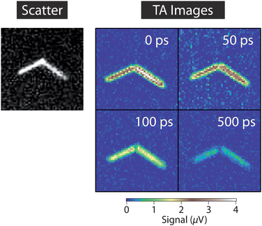 | ||
| Fig. 3 Transient absorption images of a CdSe NW taken at different time delays between the pump and probe beams. The pump and probe powers were 1.5 μW and 50 μW, respectively, and the image size is 5 × 5 μm2. The data was recorded with a lock-in time constant of 300 ms and a 1 s pixel dwell time. | ||
The data presented in Fig. 1–3 demonstrate an important attribute of transient absorption microscopy: both fluorescent and non-fluorescent nano-objects can be imaged and studied with high sensitivity. To date the systems that have been interrogated include Au nanospheres,30,34 nanorods,51–53 rings54 and dimers;55 Ag nanospheres,31,56 nanocubes37 and nanowires;57 ZnO nanostructures;35 CdTe and CdSe nanowires;36,46 Si nanowires;58 and carbon nanotubes.39,59,60 The main focus of these studies was to measure dynamical properties of the objects, rather than as a detection platform. The properties that have been studied include: the time scales for charge carrier trapping for the semiconductor materials,30,35,46 and electron–phonon coupling31,52 and dephasing of acoustic vibrational modes for the metals.30,37,51,53,57 An important conclusion from these studies is that there are large differences in the dynamics for different nano-objects in a sample. This can arise form a variety of effects, such as how the object interacts with its environment, and surface chemistry. Transient absorption microscopy has also been used to interrogate nanostructured thin film materials, such as graphene40,61,62 and conducting polymer blends.63,64 In the thin film studies information was obtained about both the morphology of the sample (through the magnitude of the signal), and the timescales for energy relaxation and charge carrier diffusion. There are fewer reports of transient absorption microscopy being used solely for imaging and detection of nanomaterials. However, a recent example is the use transient absorption microscopy to detect carbon nanotubes in mice.59
There are several attributes of transient absorption microscopy that make it a potentially useful component of the Analytical Chemist's toolkit. This technique has the ability to detect materials with either high or low emission quantum yields, in a variety of environments. The time-resolved capability of transient absorption microscopy is also a powerful aspect, providing both fundamental information about the nanostructures being interrogated, and allowing for the differentiation of metal nanostructures from semiconductors, for example.39 The data presented in this mini-review shows that metal and semiconductor nanostructures with dimensions as small as 5 nm could be detected with reasonable signal-to-noise and averaging times. Indeed, we have been able to record images and transient spectra of isolated single wall carbon nanotubes,60 demonstrating the potential of transient absorption microscopy for ultrasensitive detection.
Acknowledgements
This work was supported by the National Science Foundation through award CHE-1110560 and CHE-0946447, and the University of Notre Dame Strategic Research Initiative. The authors are also grateful to Nattasamon Petchsang and Masaru Kuno for providing the CdSe nanowire samples, and to Libai Huang for helpful discussions.References
- H. S. White, Analyst, 2012, 137, 2921 RSC.
- W. E. Moerner and M. Orrit, Science, 1999, 283, 1670–1676 CrossRef CAS.
- D. Lasne, G. A. Blab, S. Berciaud, M. Heine, L. Groc, D. Choquet, L. Cognet and B. Lounis, Biophys. J., 2006, 91, 4598–4604 CrossRef CAS.
- W. C. W. Chan, D. J. Maxwell, X. H. Gao, R. E. Bailey, M. Y. Han and S. M. Nie, Curr. Opin. Biotechnol., 2002, 13, 40–46 CrossRef CAS.
- X. Michalet, F. F. Pinaud, L. A. Bentolila, J. M. Tsay, S. Doose, J. J. Li, G. Sundaresan, A. M. Wu, S. S. Gambhir and S. Weiss, Science, 2005, 307, 538–544 CrossRef CAS.
- S. Schultz, D. R. Smith, J. J. Mock and D. A. Schultz, Proc. Natl. Acad. Sci. U. S. A., 2000, 97, 996–1001 CrossRef CAS.
- R. Hu, K. T. Yong, I. Roy, H. Ding, S. He and P. N. Prasad, J. Phys. Chem. C, 2009, 113, 2676–2684 CAS.
- C. Sonnichsen, T. Franzl, T. Wilk, G. von Plessen, J. Feldmann, O. Wilson and P. Mulvaney, Phys. Rev. Lett., 2002, 88, 077402 CrossRef CAS.
- C. F. Bohren and D. R. Huffman, Absorption and Scattering of Light by Small Particles, Wiley, 1998 Search PubMed.
- M. A. van Dijk, A. L. Tchebotareva, M. Orrit, M. Lippitz, S. Berciaud, D. Lasne, L. Cognet and B. Lounis, Phys. Chem. Chem. Phys., 2006, 8, 3486–3495 RSC.
- L. Cognet, S. Berciaud, D. Lasne and B. Lounis, Anal. Chem., 2008, 80, 2288–2294 CrossRef CAS.
- D. Boyer, P. Tamarat, A. Maali, B. Lounis and M. Orrit, Science, 2002, 297, 1160–1163 CrossRef CAS.
- S. Berciaud, L. Cognet, G. A. Blab and B. Lounis, Phys. Rev. Lett., 2004, 93, 257402 CrossRef.
- S. Berciaud, D. Lasne, G. A. Blab, L. Cognet and B. Lounis, Phys. Rev. B: Condens. Matter Mater. Phys., 2006, 73, 045424 CrossRef.
- M. Selmke, M. Braun and F. Cichos, ACS Nano, 2012, 6, 2741–2749 CrossRef CAS.
- M. Selmke, M. Braun and F. Cichos, Opt. Express, 2012, 20, 8055–8070 CrossRef CAS.
- A. Gaiduk, M. Yorulmaz, P. V. Ruijgrok and M. Orrit, Science, 2010, 330, 353–356 CrossRef CAS.
- A. Gaiduk, P. V. Ruijgrok, M. Yorulmaz and M. Orrit, Chem. Sci., 2010, 1, 343–350 RSC.
- A. Arbouet, D. Christofilos, N. Del Fatti, F. Vallee, J. R. Huntzinger, L. Arnaud, P. Billaud and M. Broyer, Phys. Rev. Lett., 2004, 93, 127401 CrossRef CAS.
- O. L. Muskens, G. Bachelier, N. Del Fatti, F. Vallee, A. Brioude, X. C. Jiang and M. P. Pileni, J. Phys. Chem. C, 2008, 112, 8917–8921 CAS.
- K. Lindfors, T. Kalkbrenner, P. Stoller and V. Sandoghdar, Phys. Rev. Lett., 2004, 93, 037401 CrossRef CAS.
- X. Hong, E. M. P. H. van Dijk, S. R. Hall, J. B. Gotte, N. F. van Hulst and H. Gersen, Nano Lett., 2011, 11, 541–547 CrossRef CAS.
- P. Kukura, M. Celebrano, A. Renn and V. Sandoghdar, J. Phys. Chem. Lett., 2010, 1, 3323–3327 CrossRef CAS.
- M. Celebrano, P. Kukura, A. Renn and V. Sandoghdar, Nat. Photonics, 2011, 5, 95–98 CrossRef CAS.
- W. S. Chang and S. Link, J. Phys. Chem. Lett., 2012, 3, 1393–1399 CrossRef CAS.
- A. N. G. Parra-Vasquez, L. Oudjedi, L. Cognet and B. Lounis, J. Phys. Chem. Lett., 2012, 3, 1400–1403 CrossRef CAS.
- A. L. Tchebotareva, P. V. Ruijgrok, P. Zijlstra and M. Orrit, Laser Photonics Rev., 2010, 4, 581–597 CrossRef.
- G. V. Hartland, Chem. Sci., 2010, 1, 303–309 RSC.
- S. H. Yue, M. N. Slipchenko and J. X. Cheng, Laser Photonics Rev., 2011, 5, 496–512 CrossRef.
- M. A. van Dijk, M. Lippitz and M. Orrit, Phys. Rev. Lett., 2005, 95, 267406 CrossRef.
- O. L. Muskens, N. Del Fatti and F. Vallee, Nano Lett., 2006, 6, 552–556 CrossRef CAS.
- D. Fu, T. Ye, T. E. Matthews, G. Yurtsever and W. S. Warren, J. Biomed. Opt., 2007, 12, 054004 CrossRef.
- W. Min, S. J. Lu, S. S. Chong, R. Roy, G. R. Holtom and X. S. Xie, Nature, 2009, 461, 1105–1109 CrossRef CAS.
- M. A. van Dijk, M. Lippitz, D. Stolwijk and M. Orrit, Opt. Express, 2007, 15, 2273–2287 CrossRef.
- B. P. Mehl, J. R. Kirschbrown, R. L. House and J. M. Papanikolas, J. Phys. Chem. Lett., 2011, 2, 1777–1781 CrossRef CAS.
- S. S. Lo, T. A. Major, N. Petchsang, L. B. Huang, M. Kuno and G. V. Hartland, ACS Nano, 2012, 6, 5274–5282 CrossRef CAS.
- H. Staleva and G. V. Hartland, J. Phys. Chem. C, 2008, 112, 7537–7539 Search PubMed.
- F. Masia, W. Langbein and P. Borri, Phys. Rev. B: Condens. Matter Mater. Phys., 2012, 85, 235403 CrossRef.
- Y. Jung, M. N. Slipchenko, C. H. Liu, A. E. Ribbe, Z. H. Zhong, C. Yang and J. X. Cheng, Phys. Rev. Lett., 2010, 105, 217401 CrossRef.
- B. A. Ruzicka, S. Wang, L. K. Werake, B. Weintrub, K. P. Loh and H. Zhao, Phys. Rev. B: Condens. Matter Mater. Phys., 2010, 82, 195414 CrossRef.
- K. L. Kelly, E. Coronado, L. L. Zhao and G. C. Schatz, J. Phys. Chem. B, 2003, 107, 668–677 CrossRef CAS.
- A. E. Siegman, Lasers, University Science Books, 1986 Search PubMed.
- M. A. van Dijk, M. Lippitz, D. Stolwijk and M. Orrit, Opt. Express, 2007, 15, 2273–2287 CrossRef.
- C. R. Carey, T. Lebel, D. Crisostomo, J. Giblin, M. Kuno and G. V. Hartland, J. Phys. Chem. C, 2010, 114, 16029–16036 CAS.
- R. R. Gattass and E. Mazur, Nat. Photonics, 2008, 2, 219–225 CrossRef CAS.
- C. R. Carey, Y. H. Yu, M. Kuno and G. V. Hartland, J. Phys. Chem. C, 2009, 113, 19077–19081 CAS.
- H. M. Zhu, N. H. Song, W. Rodriguez-Cordoba and T. Q. Lian, J. Am. Chem. Soc., 2012, 134, 4250–4257 CrossRef CAS.
- K. E. Knowles, E. A. McArthur and E. A. Weiss, ACS Nano, 2011, 5, 2026–2035 CrossRef CAS.
- A. Arbouet, D. Christofilos, N. Del Fatti, F. Vallee, J. R. Huntzinger, L. Arnaud, P. Billaud and M. Broyer, Phys. Rev. Lett., 2004, 93, 127401 CrossRef CAS.
- M. Kuno, Phys. Chem. Chem. Phys., 2008, 10, 620–639 RSC.
- P. Zijlstra, A. L. Tchebotareva, J. W. M. Chon, M. Gu and M. Orrit, Nano Lett., 2008, 8, 3493–3497 CrossRef CAS.
- H. Baida, D. Mongin, D. Christofilos, G. Bachelier, A. Crut, P. Maioli, N. Del Fatti and F. Vallee, Phys. Rev. Lett., 2011, 107, 057402 CrossRef CAS.
- P. V. Ruijgrok, P. Zijlstra, A. L. Tchebotareva and M. Orrit, Nano Lett., 2012, 12, 1063–1069 CrossRef CAS.
- R. Marty, A. Arbouet, C. Girard, A. Mlayah, V. Paillard, V. K. Lin, S. L. Teo and S. Tripathy, Nano Lett., 2011, 11, 3301–3306 CrossRef CAS.
- J. Burgin, P. Langot, N. Del Fatti, F. Vallee, W. Huang and M. A. El-Sayed, J. Phys. Chem. C, 2008, 112, 11231–11235 CAS.
- H. Baida, D. Christofilos, P. Maioli, A. Crut, N. Del Fatti and F. Vallee, J. Raman Spectrosc., 2011, 42, 1891–1896 CrossRef CAS.
- H. Staleva, S. E. Skrabalak, C. R. Carey, T. Kosel, Y. N. Xia and G. V. Hartland, Phys. Chem. Chem. Phys., 2009, 11, 5889–5896 RSC.
- M. A. Seo, S. A. Dayeh, P. C. Upadhya, J. A. Martinez, B. S. Swartzentruber, S. T. Picraux, A. J. Taylor and R. P. Prasankumar, Appl. Phys. Lett., 2012, 100, 071104 CrossRef.
- L. Tong, Y. X. Liu, B. D. Dolash, Y. Jung, M. N. Slipchenko, D. E. Bergstrom and J. X. Cheng, Nat. Nanotechnol., 2012, 7, 56–61 CrossRef CAS.
- B. Gao, G. V. Hartland and L. B. Huang, ACS Nano, 2012, 6, 5083–5090 CrossRef CAS.
- L. B. Huang, G. V. Hartland, L. Q. Chu, Luxmi, R. M. Feenstra, C. X. Lian, K. Tahy and H. L. Xing, Nano Lett., 2010, 10, 1308–1313 CrossRef CAS.
- B. Gao, G. Hartland, T. Fang, M. Kelly, D. Jena, H. L. Xing and L. B. Huang, Nano Lett., 2011, 11, 3184–3189 CrossRef CAS.
- G. Grancini, D. Polli, D. Fazzi, J. Cabanillas-Gonzalez, G. Cerullo and G. Lanzani, J. Phys. Chem. Lett., 2011, 2, 1099–1105 CrossRef CAS.
- C. T. O. Wong, S. S. Lo and L. Huang, J. Phys. Chem. Lett., 2012, 3, 879–884 CrossRef CAS.
Footnote |
| † Electronic supplementary information (ESI) available. See DOI: 10.1039/c2an36097g |
| This journal is © The Royal Society of Chemistry 2013 |