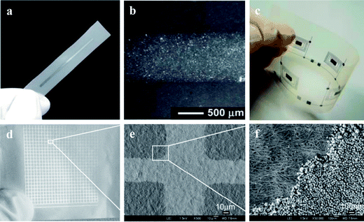
Transparent paper: fabrications, properties, and device applications
Received
8th September 2013
, Accepted 8th November 2013
First published on 11th November 2013
Abstract
Although paper electronics is a compelling concept, the large surface roughness and opaqueness of most paper substrates has hindered its development from a dormant idea to a thriving technology. A recent demonstration of transparent paper with nanoscale surface roughness has revived an interest in using renewable cellulose substrates for electronics and optoelectronics. In this short review, we will first summarize the recent progress of transparent paper electronics through structure engineering. We will also discuss the properties and functionalization of transparent paper, such as surface roughness, printability, thermal stability, etc. Finally, we will summarize the recent achievements on proof-of-concepts of transparent paper, which pave the way for next-generation green electronics fabricated with roll-to-roll printing methods. Advantages of transparent paper over traditional flexible plastic substrates and its challenges will also be discussed.
 Hongli Zhu | Hongli Zhu is currently a postdoctoral research associate with Prof. Liangbing Hu at the University of Maryland, focusing on innovations for transparent flexible electronics and energy storage. She received her PhD degree at South China University of Technology in 2009, and researched processing of degradable and renewable biomaterials from natural wood with Prof. Gunnar Henriksson at the Royal Institute of Technology in Sweden from 2009 to 2011, including nanocellulose and naocomposite. |
 Zhiqiang Fang | Zhiqiang Fang received his B.S. degree from Shannxi University of Science and Technology majoring in Light Chemical Engineering in 2006. He is now a Ph.D. candidate at the State Key Laboratory of Pulp and Paper Engineering for the South China University of Technology, and is currently a Ph.D. candidate at the Materials Science and Engineering Department at the University of Maryland. His current research interests include nanomaterials and nanostructures, application of paper on flexible electronics and energy storage devices, and flexible devices. |
 Colin Preston | Colin Preston received his B.S. in physics from Villanova University in 2011. He is currently a Ph.D. candidate in the Materials Science and Engineering Department at the University of Maryland. His current research interests include nanomaterials and nanostructures, energy storage and conversion, carbon nanotubes, printed electronics, and flexible devices. |
 Yuanyuan Li | Yuanyuan Li received her M.S. from the College of Light Industry Science and Engineering at Nanjing Forestry University in 2011. She is currently an exchange Ph.D. candidate student at the University of Maryland. Her research focus on multifunctional fibers and flexible electronics in Dr. Liangbing Hu’s group. |
 Liangbing Hu | Liangbing (Bing) Hu received his B.S. in applied physics from the University of Science and Technology of China (USTC) in 2002. He did his Ph.D. in experimental physics at UCLA. In 2006, he joined Unidym Inc (www.unidym.com) as a co-founding scientist, and his role was the development of roll-to-roll printed carbon nanotube transparent electrodes and device integrations. As a postdoc at Stanford from 2009 to 2011, he worked on various energy storage and conversion devices. Currently, he is an assistant professor at University of Maryland College Park. His research interests include energy science and devices, flexible electronics and nanomanufacturing. |
Broader context
The mechanical properties of flexible electronic devices greatly depend on the substrate that hosts the device. Since the rise of flexible electronics in the 1970s, plastics have dominated the industry as the substrate for these devices due to their flexibility, lightweight, and durability. A concern with plastics is that they are manufactured from petroleum-based materials and they are not biodegradable, making them environmentally hazardous to produce and dispose. This has led to a green initiative in pursuit of recyclable or environmentally friendly alternatives to plastic substrates to host flexible electronics. A compelling technology that has emerged from recent studies is cellulose-based substrates that offer an earth-abundant, recyclable, and cleanly manufactured option for use in flexible devices. The unique layered structure of these paper-based structures enables numerous engineering possibilities and device applications. For instance, the development of transparent paper may usher in a new era of flexible optoelectronic devices that are amenable to roll-to-roll printing and are environmentally friendly. Transparent paper has already begun to gain significant research interest in recent years, which has yielded transparent paper substrates with various tailored optical properties that are engineered for new functionalities and that introduce new flexible devices. This review is a summary of the contemporary status and prospected future of transparent paper technology for flexible, foldable, and environmentally friendly electronics.
|
1. Introduction
Paper has been used in everyday life for more than 2000 years. The earth-abundance of the cellulose materials, easy handling and process ability, biocompatibility and biodegradability, compatibility with fast roll-to-roll printing, low-cost, etc. sustain paper as ubiquitously used material for various purposes. Paper is specifically an ideal substrate for low-cost printed macroelectronics with applications complimentary to high-end silicon-based electronics.1–5 Regular paper is made of cellulose fibers with a diameter in the range of 20–50 μm. The large surface roughness, porous structure, and optical opaqueness of regular paper are intrinsic barriers to hosting electronic devices on the surface of this material. Ways to overcome these problems include smoothing the roughness by supercalendering, coating a layer on the surface,6–11 or fabricating devices on other flat substrates and then transferring or laminating them on paper.12–14 Nevertheless, various devices on paper have been demonstrated, including field-effect transistors,15–18 organic solar cells,12,19–22 and chemical and biological sensors.23–25 Smoothing the paper surface with a polymer coating decreases the substrate printability; the transfer-printing method to make devices on paper is complicated and incompatible with low-cost printed electronics.
Methods for re-engineering paper through new structures that can solve the intrinsic problems of paper substrate have been developed. The cellulose research community has already established a significant fundamental understanding of the cellulose fiber materials. It is amazing that the natural cellulose fibers with a diameter of 20–50 μm is made of thousands of microfibril with a diameter of a few or tens of nanometers that can form a smoother film that scatters less light than regular paper. These cellulose fibers can even be dissolved and then used to make transparent films by the same process as plastic industry. Yano et al. made a breakthrough in transparent paper technology by utilizing nanofibrillated cellulose (NFC) in 2005.26,27 Zhang et al. also demonstrated transparent paper with dissolved cellulose.28–33 Studies by Fernandes et al. report a new process to prepare NFC fibers, hence fabricate transparent paper more quickly with less energy.34–42 These new paper substrates are made of the same material—cellulose, as regular paper, but incorporate different dimensions and functional groups to form highly transparent (>90%) and smooth (<10 nm) paper substrates. A range of electronic devices on transparent paper substrate have recently been demonstrated, including organic light-emitting diodes (OLED), organic solar cells, touch screens, thin film transistors (TFTs), and antennas.43–55 These exciting results show that transparent paper not only matches the desirable properties of plastic substrates, but introduces new characteristics such as recyclability, enhanced printability, and enhanced flexibility that can even facilitate bending and eased folding. The goal of this review is to summarize the recent progress in transparent paper, including materials processing, fundamental characterizations and functionalization, proof-of-concepts, and challenges for further development. In this review, transparent paper refers to any cellulose-based film with an optical transmittance up to 60%.
2. Cellulose materials as the building blocks
Cellulose is the most abundant biopolymer on the earth. Wood fibers are composed of 40–45% cellulose, which is produced in nature via photosynthesis and ubiquitously used in the everyday life.56 The cell wall of natural wood fibers has a 3 dimensional (3D) hierarchical structure designed for the metabolic ion transportation and to possess mechanical stability, as shown in Fig. 1(a).57 The cell wall thickness of the wood fiber is around 4 μm, which is composed of thousands of microfibril bundles with a diameter larger than 15 nm and length larger than 2 μm.58 The microfibril bundles are composed of microfibril cellulose (MFC) and nanofibril cellulose (NFC). MFC is delaminated from wood pulp through mechanical treatments before and/or after enzymatic or chemical pretreatment, which has a diameter of 5–60 nm with a length of several micrometers.59 The terminology ‘MFC’ was coined by Sandberg et al. at ITT Rayonnier, USA and widely used in academic and commercial literature in the beginning.60 Over time, the term ‘NFC’ is dominated. The borderline between MFC and NFC is hard to define; however MFCs are attributed to a broader size distribution for nano-sized fibrils, fibrillar fines, fiber fragments, and fibers, while NFCs refer to nano-sized fibers.61Fig. 1(b) shows a SEM image of microfibril network covering the outside layer of the tracheid cell wall. The natural wood fiber has a mesoporous structure because of the hierarchical structure, which plays a critical role for the electrolyte reservation and ion transportation in the energy storage device.57,62,63 The MFCs grow together into microfibril bundles to reduce the free surface energy. The elementary fibrils with a diameter of 1.5–3.5 nm are defined as a universal structural unit of natural cellulose fiber, as the same biological unit for bacterial cellulose, cotton, and wood fibers.64 At the molecular scale, cellulose biopolymers have a linear chain structure consisting of D-glucose unit via β (1–4) linkage with a degree of polymerization (DP) from 300 to 10![[thin space (1/6-em)]](https://www.rsc.org/images/entities/char_2009.gif) 000.65 Natural cellulose is usually found in a mixture with random amorphous hemicellulose, and bio ‘glue’ lignin. Fig. 1(c) is the electron microscope image of the cross section of a spruce-fiber cell wall,59 from which the microfibrils are well defined. The hierarchical structure of wood fibers makes it possible to liberate the bio nanofiber from wood through disintegration process. NFC has many unique properties, such as excellent mechanical strength, interesting light scattering behavior, large specific surface area (100–200 g m−2), high aspect ratio (100–150), and active surface modification properties.60,66 Applying NFC to make transparent flexible electronics has attracted worldwide interest for its high transmittance, tunable optical properties, excellent flexibility, and light weight.67
000.65 Natural cellulose is usually found in a mixture with random amorphous hemicellulose, and bio ‘glue’ lignin. Fig. 1(c) is the electron microscope image of the cross section of a spruce-fiber cell wall,59 from which the microfibrils are well defined. The hierarchical structure of wood fibers makes it possible to liberate the bio nanofiber from wood through disintegration process. NFC has many unique properties, such as excellent mechanical strength, interesting light scattering behavior, large specific surface area (100–200 g m−2), high aspect ratio (100–150), and active surface modification properties.60,66 Applying NFC to make transparent flexible electronics has attracted worldwide interest for its high transmittance, tunable optical properties, excellent flexibility, and light weight.67
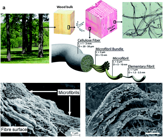 |
| | Fig. 1 (a) Schematic to show the hierarchical structure of wood fibers. (b) SEM image of the network of microfibrils covering the outer wall layer of the fiber. (c) SEM image of the cross section of spruce fiber to show the microfibrils with a diameter of ∼20 nm.57,59,61 | |
The NFC can be isolated from the natural fiber with chemical, enzymatic, and mechanical treatments.68–70 In 1983, Herrick et al. at ITT Rayonnier first reported the manufacture of NFC through mechanical high pressure homogenizers.60 The high-energy consumption at 25![[thin space (1/6-em)]](https://www.rsc.org/images/entities/char_2009.gif) 000 kW h per ton is a hurdle for the development and application of NFC in industry. Enzymatic pretreatment, chemical pretreatment, and refining have been applied in conjunction or as single stage treatments to break up the structure of the raw material, hence reducing the energy demand to produce NFC.71–75 Zhu et al. reported a novel energy-efficient method named “nanopulping” with an energy consumption at 443 kW h per t.76 The NFCs exhibit gel-like properties in water at low concentrations (1–2%) (Fig. 2(a)), hence the NFC is widely used to prepare hydrogels, aerogels, and thickeners in food.59,77–79 Due to the large presence of hydroxyl groups, the pristine nanocellulose tends to aggregate, especially when they are dried. Surface modification is employed, such as oxidation the hydroxyl group to carboxyl group via TEMPO treatment, to improve the stability and better dispersion. There are other cellulose nanofibers from plant, tunicate, bacterial, and algae that are not derived from wood.80 The bacterial cellulose is quite pure with a larger water content and longer chain length. Fig. 2(b) shows the electron microscope image of NFC with an average diameter of 30 nm (20–60 nm range) obtained by mechanical fibrillation from the hardwood sulfite pulps.44 The high aspect ratio along with the disordered amorphous region and ordered crystalline region in NFC grant the nanopaper with both excellent flexibility and high mechanical strength. The nanopaper made from NFC is widely used as a flexible transparent biodegradable substrate for advanced electronic and energy devices.45,49,53 The other important group of nanocellulose is the cellulose nanocrystal (CNC), which is isolated by hydrolyzing away the amorphous fraction and leaving the pure crystalline segments. Compared to the NFC, the CNC has higher crystallinity and a smaller aspect ratio. This gives CNC excellent mechanical properties that make it suitable for reinforcing materials in composite material, such as filler, plastic, and polymer. The flexibility of CNC is less than NFC, which limits the application of CNC as a substrate in flexible electronics.
000 kW h per ton is a hurdle for the development and application of NFC in industry. Enzymatic pretreatment, chemical pretreatment, and refining have been applied in conjunction or as single stage treatments to break up the structure of the raw material, hence reducing the energy demand to produce NFC.71–75 Zhu et al. reported a novel energy-efficient method named “nanopulping” with an energy consumption at 443 kW h per t.76 The NFCs exhibit gel-like properties in water at low concentrations (1–2%) (Fig. 2(a)), hence the NFC is widely used to prepare hydrogels, aerogels, and thickeners in food.59,77–79 Due to the large presence of hydroxyl groups, the pristine nanocellulose tends to aggregate, especially when they are dried. Surface modification is employed, such as oxidation the hydroxyl group to carboxyl group via TEMPO treatment, to improve the stability and better dispersion. There are other cellulose nanofibers from plant, tunicate, bacterial, and algae that are not derived from wood.80 The bacterial cellulose is quite pure with a larger water content and longer chain length. Fig. 2(b) shows the electron microscope image of NFC with an average diameter of 30 nm (20–60 nm range) obtained by mechanical fibrillation from the hardwood sulfite pulps.44 The high aspect ratio along with the disordered amorphous region and ordered crystalline region in NFC grant the nanopaper with both excellent flexibility and high mechanical strength. The nanopaper made from NFC is widely used as a flexible transparent biodegradable substrate for advanced electronic and energy devices.45,49,53 The other important group of nanocellulose is the cellulose nanocrystal (CNC), which is isolated by hydrolyzing away the amorphous fraction and leaving the pure crystalline segments. Compared to the NFC, the CNC has higher crystallinity and a smaller aspect ratio. This gives CNC excellent mechanical properties that make it suitable for reinforcing materials in composite material, such as filler, plastic, and polymer. The flexibility of CNC is less than NFC, which limits the application of CNC as a substrate in flexible electronics.
 |
| | Fig. 2 (a) Photograph of a NFC hydrogel (courtesy: Innventia AB, Sweden). (b) SEM image of NFC. (c) Fluid SPM image of CNCs on surface treated mica.44,65,81 | |
3. Structures and fabrications of transparent paper
Wood pulp for the production of transparent paper is primarily comprised of cellulose since most lignin and hemicellulose is removed during the pulping and bleaching procedure. Cellulose is polymerized by a repeating unit of glucose and have ether, hydroxyl, carbon–carbon, and carbon–hydrogen bonds in the cellulose structure that do not adsorb light in the optical wavelengths.80 Lack of color absorption renders the pure cellulose colorless. Paper is a fibrous network permeated by micro-sized air cavities. The different refractive indices of the cellulose and air (1.5 and 1.0, respectively) cause the light scattering at the fiber surfaces and manifest as the opacity of paper. Methods to make paper transparent primarily involve fiber treatment, paper processing, or combination of both.82 Fiber treatments include a change in the refinement of wood fibers, homogenization, and chemical dissolution of fibers, while paper processing refers to impregnation, coating, surface selective dissolution of fibers and supercalendering.28,34,39,40,46,47,83–91Fig. 3(a) shows the schematic of transparent nanopaper fabrication via a filtration process.36 The 0.2% microfibrillated cellulose fiber suspension was filtrated through a 0.65 μm filter membrane with a semiautomatic sheet former (Fig. 3(a), step 1). The formed gel “cake” is peeled from the membrane and stacked first between two woven metal cloths and then two paper carrier boards (Fig 3(a), step 2). This package was placed in the sheet dryer for 10 min at 93 °C (Fig. 3(a), step 3).
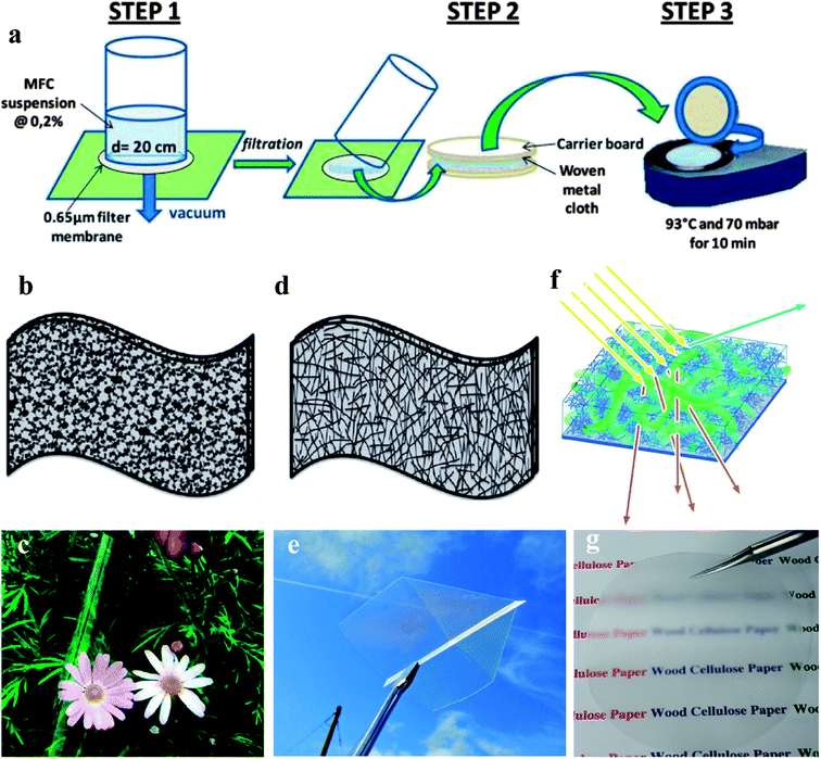 |
| | Fig. 3 (a) A schematic to show the transparent paper fabrication process via vacuum filtration. (b) A schematic (c) and an image of RCF. (d) A schematic and (e) an image of nanopaper with cellulose nanofibers. (f) A bilayer schematic structure and (g) an image of transparent hybrid paper with a regular cellulose fibers and NFCs. The blue bottom layer contains 100% NFC and the top layer is hybrid layer comprised of NFC and regular cellulose fibers.28,36,39,53,54 | |
Commercial transparent papers made of micro-sized cellulose fibers or regenerated cellulose, such as tracing paper, glassine, parchment paper, wax paper, and cellophane, are widely applied in wrapping, food packaging, release labels, weighing paper, bookbinding, drawing, electrical insulator and so on. Transparent paper was introduced in the mid-19th century by combining oils, gums, resins, varnishes and mixture with the raw laid or woven paper.83 In 1846 chemically treated transparent paper was first developed by subjecting formed paper to a chemical solution (such as sulphuric acid or dilute ammonia) to selectively dissolve part of the fibers followed by several washes. A crucial approach to make transparent paper was developed at the end of 19th century by using intensive beaten fibers followed by compacting the formed paper in calender,83 and the optical transmittance of transparent paper could be further enhanced by impregnation or coating of oils, gums, wax and resins.83,84 In addition, viscose technology has been proposed to produce regenerated cellulose film (RCF) with excellent transparency for more than 100 years. Cellulose is entirely dissolved in a solution to make viscose, which is then extruded through a slit into regenerated solution to form RCF. Cross et al. first prepared the RCF using viscose in the lab.92 Since then many scientists focused on using environmentally friendly and economical solutions to dissolve the cellulose fibers in various solutions, such as 1-ethyl-3-methylimidazolium phosphorous methyl ester, alkali-urea low temperature aqueous system or N-methylmorpholine-N-oxide (NMMO), and produce RCF with entire dissolved cellulose solution.28,29,32,33,88,93,94 RCF films with dissolved cellulose match the appearance of plastic substrates. Fig. 3(b) illustrates the schematic of RCF, which was cast from entire dissolved cellulose. Transparent RCF with an optical transparency up to 90% at 600 nm as well as a tensile strength of 150 MP is presented in Fig. 3(c).28 Although transparent papers are abundantly available in the commercial market, there are still few reports of their applications in flexible electronics.
Since Herrick and Turbak first disintegrated cellulose nanofibers from wood pulp in 1983 there has been extensive attention dedicated to novel transparent paper made from cellulose nanofibers,60,70,95 Taniguchi et al. first presented a film manufacturing from microfibrillated cellulose fibers with a diameter in the range of 20–90 nm in 1998.96 Ever since efforts to produce transparent paper based on cellulose nanofibers by vacuum-filtration or casting has intensified.41,97,98Fig. 3(d) is a schematic of nanopaper made of cellulose nanofibers, and a picture of nanopaper is displayed in Fig. 3(e). The first study on the potential application of nanopaper with high optical transmittance towards electronic devices was published by Yano's group in 2009.39 In a typical experiment, wood fibers were liberated into smaller fibers, with a diameter less than 100 nm. Cellulose nanofibers were dispersed in water with a concentration of 0.2 wt%, and then a wet film was fabricated with a filtration. The wet film was dried by applying mechanical pressing simultaneously with wire meshes. Mechanical polishing and immersing in resin were also used to further improve the optical transmittance of the nanopaper.39 Isogai et al. applied a TEMPO oxidization system to introduce carboxyl groups into the cellulose and make it easy to disintegrate NFC from fiber with the final mechanical treatment. The disintegrated cellulose nanofibers were then used to produce a film by vacuum filtration that was more transparent and possesses higher gas barrier property.41 An optically transparent film was also fabricated by Zhu and his co-workers using cellulose nanofiber extracted from cellulosic solid residue that was recovered from the hydrolysates of acid hydrolysis of hardwood pulp.99
In addition, transparent composites fabricated by impregnating cellulose nanofibers paper into various resins are well documented. Yano's group developed the fabrication of transparent composites paper reinforced with cellulose nanofibers, including wood cellulose nanofiber, bacterial nanofibers.46,48,100–102 Nanofiber paper was fabricated through a filtration of wood cellulose nanofibers with fiber content of 0.2 wt% or by compressing a BC pellicles. The dried nanopaper was dipped into transparent thermosetting resins (such as acrylic, epoxy, or phenol-formaldehyde) to improve the transparency of the composites. Cellulose nanocrystal103 and chitin nanofibers104 were used as reinforcing agent to make transparent composites. Transparent paper made of cellulose nanofibers or cellulose nanofiber based composites has a very high optical transmittance and strong mechanical strength; however, it consumes time and energy to prepare NFCs and nanopaper due to low drainability of nanofibers suspension. This is especially serious for the TEMPO treated cellulose nanofibers that have many surface charges, which greatly limits its commercial application.
To commercialize transparent paper made of cellulose nanofibers, scientists all over the world have endeavored to perfect efficient manufacturing techniques. Sehaqui36et al. developed a fast procedure for preparing nanopaper using a semiautomatic sheet former. One nanopaper substrate with a thickness of 60 μm took 1 hour to filter, and the nanopaper had a tensile strength of 232 MPa and surface roughness of 21.9 nm, but the transparency of nanopaper was only reported to be 42.0% at wavelength of 600 nm. Österberg et al.35 combined an overpressure filtration with hot-pressing to rapidly prepare nanopaper with a tensile strength of 230 MPa, yet no optical data was reported. A rapid method to prepare a nanopaper substrate in 10 minutes was reported by Varanasi and Batchelor,37 tensile index of the nanopaper was 94.2 kN m kg−1, but no optical transmittance was reported in this study. Recently, Hu et al. developed a bilayer structural hybrid transparent paper with microsized fibers filled with nanofibers.54 As illustrated in Fig. 3(f), wood fibers were bleached sulfate softwood pulp. Nanofibers were derived from wood fibers through a TEMPO treatment and homogenization. The mixture was then filtered through a membrane and the resulting wet film was then carefully placed between filters and dried under mechanical pressure. An image of transparent hybrid paper is in Fig. 3(g). Compared with nanopaper, hybrid paper needs significant less energy and time for fabrication, which benefits the nanomanufacturing of transparent paper substrates for commercial applications. Although significant progress towards fast fabrication of highly transparent and superiorly smooth paper has been made, there is still a lack of efficient methods to manufacture transparent paper on a large scale that limits widespread application to flexible electronics.
4. Properties of transparent paper
4.1 Tailored optical properties through structural engineering
One of the intriguing properties of transparent paper substrates is their high optical transmittance and tunable optical haze. Regular paper made from common fibers is opaque, but when the fibers go down to nanoscale, the paper becomes transparent due to denser structure. Fig. 4(a) illustrates a horizontal laser beam with a 650 nm wavelength incident from the left with the first bottle contains pure distilled water as the reference. It is clear from the figure that the light scattering increases dramatically with an increase in fiber diameter from 10 nm to 25 μm. Zhu et al. modeled the electromagnetic scattering cross-section for fibers with 25 nm and 50 nm diameters. The result indicates that the light scattering decreases sharply with increases in fiber size, which agrees well with Rayleigh's Scattering theory; σsca ∝ D,3 where D is the fiber diameter and σsca is the scattering cross section.67,105 Although the back light scattering is suppressed by the nanopaper surface, the individual nanofibers promote forward scattering as shown Fig. 4(b), which causes the nanopaper to display higher haze than plastic such as PET (polyethylene terephthalate). Fig. 4(c) and (d) further demonstrates the forward light scattering is enhanced with an increase of nanofiber diameter. The nanopaper made from 10 nm and 50 nm fibers have a similar diffusive transmittance at 92–93%, but the specular transmittance of nanopaper made from 50 nm fibers is much lower than nanopaper made from 10 nm fibers. The ratio of diffusive to specular transmittance determines forward light scattering. Since there is greater forward light scattering of the 50 nm sample than the 10 nm sample, the 50 nm nanopaper is considered to have larger haze than 10 nm sample, as seen in Fig. 4(e).67 The cavities in nanoscale among nanofibers are the main cause for the large haze value. In order to decrease the optical haze for some display applications, one strategy is to fill the cavities with polymer such as resin and polyvinyl alcohol (PVA) by impregnation. The ability to tune the optical haze is critical for various applications. High optical haze is preferred for thin film solar cells and outdoor display applications,106 while high optical clarity (low haze) is preferred for most indoor displays.
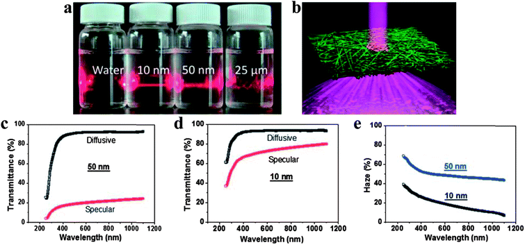 |
| | Fig. 4 (a) An image of light scattering behavior of cellulose dispersions with different fiber diameters. (b) Schematic of the light scattering effect from the nanopaper. (c) Specular and diffusive transmittance of nanopaper made from 50 nm fibers. (d) Specular and diffusive transmittance of nanopaper made from 10 nm fibers. (e) The haze for nanopaper made from 50 nm and 10 nm fibers respectively. All the papers have the same thickness of 40 μm.49,67 | |
The optical haze and transmittance of transparent paper can be tuned by the porosity and the size of fiber. It is critical to design transparent paper with tunable optical properties with low-cost processes. Hu et al. recently investigated highly transparent and hazy paper with hybrid cellulose.54 The regular wood fibers act as a scaffold of the paper, while NFC fills the voids to decrease the light scattering. Since NFC has a similar light refraction index ∼1.5 with the regular fiber as opposed to air, the paper may be tuned from opaque to transparent depending on the degree of space filled with NFC. As shown in Fig. 5, the transmittance and haze property can be tuned with the ratio of NFC within paper. In Fig. 5(a), the total transmittance of the hybrid paper improves with the increase of NFC ratio. The hybrid paper has the same transmittance of 91.5% with PET when the concentration of NFC in the paper reaches 60%. The haze of the hybrid paper is much higher than PET (Fig. 5(b)). The presence of both high transmittance and high haze will be desirable for optoelectronic devices such as thin film solar cells. The efficiency of a thin film solar cell will increase with the enhanced light trapping. Another application of hybrid paper is used as an outdoor electronic display, such as a global positioning system (GPS), ipad, or cellphone. The larger haze lessens the glare generated from a strong light source. Hybrid paper depends on a less time consuming manufacturing method than pure nanopaper, which renders it cheaper and thus more scalable. Hybrid paper also has better malleability and shape stability than nanopaper since it uses regular fibers as a reinforcing backbone.
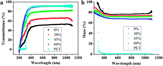 |
| | Fig. 5 (a) Total transmittance vs. wavelength for hybrid papers with different weight ratios of NFC to regular fibers. (b) Transmission haze vs. wavelength for hybrid paper with various weight ratios of NFC.54 | |
4.2 Mechanical properties
The mechanical properties of substrates play an important role for the comprehensive device. Fig. 6(a) is a field effect SEM image of a nanopaper dried after filtration from a water suspension. An SEM image shows that the NFC is randomly distributed in plane (Fig. 6(a)). The nanopaper looks like a thin plastic film to the naked eye, but in fact it has a unique porous structure in the nanoscale that is totally different with traditional transparent substrates. The typical pore size is 10–50 nm (Fig. 6(a)).97 The all fiber porous network structure gives the nanopaper excellent flexibility and can be folded to form 3D structures for paper origami. The cross section (Fig. 6(b)) shows that the nanopaper has a layered nanoporous structure.44,107 This structure enables the nanopaper to effectively release the stress in the active layers generated by bending the electronics devices.44,45,53
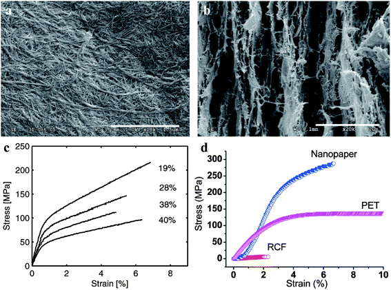 |
| | Fig. 6 (a) SEM image of a nanopaper surface. (b) SEM image of a nanopaper cross section. (c) Stress–strain curves for nanopaper with different porosities. Cellulose with DP 800 was used. (d) Comparison of tensile strength for different transparent substrate, including PET, regenerated cellulose film, and nanopaper.53,97 Note that the maximum strain for PET is up to 81%. | |
Another interesting property of transparent nanopaper is the remarkable high tensile strength, Young's modulus, toughness, and strain to failure due to the tightly packed nanofibrillar network and numerous fiber–fiber hydrogen bonds. These properties manifest themselves as making nanopaper ten times stronger than regular paper.45,53 Nanopaper is also light and flexible while super strong. Fig. 6(c) shows the typical stress–strain curve for nanopaper with different porosities; it is clear that the higher porosity has the lower tensile strength. The nanopaper with 19% porosity formed from a water suspension has the highest tensile strength at 205 MPa. Along with its porosity, nanopaper's tensile strength relates directly to the DP of cellulose and its fabrication process.97,108Fig. 6(d) compares the stress–strain curves for nanopaper, RCF, and PET. The nanopaper has a higher tensile stress than PET, but a lower strain-to-failure. The RCF has a weaker tensile strength due to its microstructure and cellulose crystalline II component, which is weaker than crystalline I.53 Note that the nanopaper is made from NFC in crystalline I. The high mechanical strength gives nanopaper huge potential in roll-to-roll printed electronics.
4.3 Thermal properties
Thermal properties of transparent paper are quite important for its application in flexible electronics. Most fabricated devices undergo a heat treatment at a temperature of approximately 150–200 °C to obtain the maximum performance of electronic devices.109 Transparent paper must withstand the processing temperature without wrinkling, tinting, or thermally decomposing. The DP of original cellulose begins to decrease around 250 °C, and extensive degradation of cellulose occurs when the temperature is over 300 °C.110,111 Here we will discuss the thermal chemical degradation and coefficient of thermal expansion (CTE) of transparent paper, which can be tested by thermogravimetric analysis (TGA) and thermomechanical analysis (TMA).
A decrease in the initial decomposed temperature of cellulose was observed when it was tested by TGA due to a change of particle type and surface modification.80 Isogai and co-workers found the thermal decomposition temperature (Td) decreased with an introduction of sodium carboxyl group into cellulose by TG analysis.112Fig. 7(a) displays the TG curves of original cellulose, TEMPO-oxidized cellulose with sodium carboxyl group, and TEMPO-treated transparent nanopaper with sodium carboxyl group, and their respective corresponding Td was 275 °C, 222 °C, and 211 °C. They also proposed several approaches to improve the thermal stability of TEMPO-oxidized cellulose by using ion exchange treatment or methyl esterification. A cellulose nanopaper with a high thermal stability that can be used to fabricate conductive circuits was presented by Nogi et al. in 2013.107 They used dissolving sulfite pulps to produce cellulose nanofibers by mechanical treatment. As shown aforementioned cellulose nanofibers and pulp paper was quite stable, but these properties were altered for photo paper when it was exposed to various processing temperatures and treatment times. Specifically, Nogi and his colleagues studied the influence of heating treatments on the optical properties and surface roughness of transparent paper.109 The optical transmittance of transparent paper remained unchanged, and no obvious change of the surface morphology was observed in Fig. 7(c) after it was treated at 150 °C for different processing times.
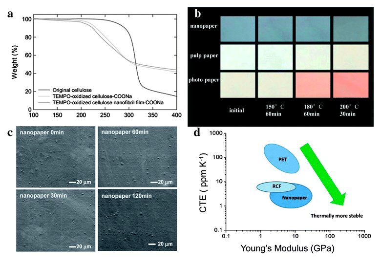 |
| | Fig. 7 (a) TGA of original cellulose, TEMPO-oxidized cellulose with sodium carboxyl group and TEMPO-oxidized cellulose film with sodium carboxyl group. (b) Digital image of photo paper, pulp paper, and nanopaper under the treatment of various temperatures. (c) SEM images of the surface of nanopaper when it exposed to 150 °C for different time. (d) Coefficient of thermal expansions vs. Young's modulus.53,107,109 | |
The CTE of crystalline cellulose in the axial direction is around 0.1 ppm K−1, which is more than an order of magnitude lower than plastics, most metals, and ceramics.88,100 The optically transparent paper made of cellulose nanofibers has a CTE of <8.5 ppm K−1, which is much lower than plastic (CTE, ∼50 ppm K−1). This is desirable for displays since it can maintain the dimensional stability under thermal processing condition.39,113 The Ashby plot of CTE vs. Young modulus is shown in Fig. 7(d).53 Nanopaper fabricated by cellulose nanofibers shows lowest CTE compared to regenerated cellulose film and PET, which represents it has the potential to replace current plastic to fabricate flexible electronics.
4.4 Surface roughness, shape stability, wicking etc.
Electronics such as transistor, OLED, and radio frequency identification (RFID) et al., have a layered structure, and the thickness of the middle layer is usually lower than 1 μm. The device will short or have a significant leakage problem if the roughness of the substrate is at micrometer scale; this is the challenge for electronics on regular paper. The transparent paper made from NFCs with diameter 5–10 nm has extremely low surface roughness due to the small fiber diameter. From the AFM height image and a line scan data shown in Fig. 8(a), we can see the maximum roughness depth Rmax is 5 nm and root mean square roughness (RMS) is 1 nm. The low surface roughness makes it easy to fabricate electronics directly on nanopaper.45,53 Other kinds of transparent paper can also have a very low surface roughness that is suitable for electronic device applications.
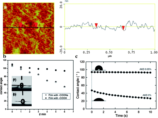 |
| | Fig. 8 (a) AFM image and a scanning line of nanopaper to show its low surface roughness, (b) contact angle vs. time for a cellulose film in acid and alkali solution. (c) Contact angle of nanopaper before and after AKD treatment.41,45,91 | |
The nanopaper has hydrophilic properties due to the large hydroxyl group in the cellulose chain, which renders nanopaper to have poor shape stability after repeated wetting and drying. Nanopaper can be hydrophobized with a surface modification to change the wettability. In Fig. 8(b), the nanopaper film with carboxyl groups in the acid has higher hydrophobicity than in the sodium due to the formation of ester bonds between hydroxyl groups and carboxyl groups in the acid.91 In Fig. 8(c), the hydrophobization is achieved by simple soaking treatments in the alkylketene dimer (AKD) dispersion.114 Compared to hydrophobicity, some devices require transparent paper to possess good wicking property, such as paper microfluidics.115,116 Microfluidics is a diagnostic device that preciously controls and manipulates the fluid in a sub-micrometer scale. The paper microfluidics is potentially attractive for its ability to wick fluids via capillary force, portability, disposability, foldability, and is ubiquitously available in various forms.24,117,118 Though the nanocellulose has numerous hydroxyl groups, the nanopaper has low porosity with small pore sizes that render the nanopaper poor wicking properties. Solvent exchange and freeze drying can be used to increase the porosity and enhance wicking properties.97 The exposed high content of active hydroxyl group on nanocellulose surface make the nanocellulose can be readily modified to have tailored properties.
4.5 Comparison with other substrates
Flexible printed electronics are important because of their advanced commercial attributes, but more importantly for their amenability to low cost, large scale, roll-to-roll manufacturing capability. The substrate is one major component of the electronic device. The properties of the substrate will ultimately determine if the device will be flexible or rigid, heavy or light, transparent or opaque, and if it can be applied to roll-to-roll processing. Regular paper and plastic are two common flexible substrates for printed electronics, and nanopaper is an emerging transparent and flexible substrate.44,45,53Table 1 is a comparison of nanopaper, regular paper, and plastic.45 Plastic is an unsustainable petroleum-based product that causes ‘white pollution’. Any wood based substrate such as regular paper and nanopaper is renewable, recyclable, and biodegradable, leaving a negligible environmental footprint. Paper also has good shape stability under high temperatures for the cellulose has low CTE. Paper also has better printability than plastic. Nanopaper possesses high optical transmittance and excellent mechanical properties, including high tensile strength, large Young's modulus, and a small bending radius. Nanopaper meets the requirements for device fabrication, environmental sustainability.
Table 1 Comparison of nanopaper, traditional paper, and plastic45,53,80,97,119
| Characteristics |
Nanopaper |
Traditional paper |
Plastic |
| Surface roughness (nm) |
5 |
5000–10![[thin space (1/6-em)]](https://www.rsc.org/images/entities/char_2009.gif) 000 000 |
5 |
| Porosity (%) |
20–40 |
50 |
0 |
| Pore size (nm) |
10–50 |
3000 |
0 |
| Optical transparency at 550 nm (%) |
90 |
20 |
90 |
| Max loading stress (MPa) |
200–400 |
6 |
50 |
| Coefficient of thermal expansion (CTE) (ppm K−1) |
12–28.5 |
28–40 |
20–100 |
| Printability |
Good |
Excellent |
Poor |
| Young modulus (GPa) |
7.4–14 |
0.5 |
2–2.7 |
| Bending radius (mm) |
1 |
1 |
5 |
| Renewable |
High |
High |
Low |
5. Functionalization of transparent paper
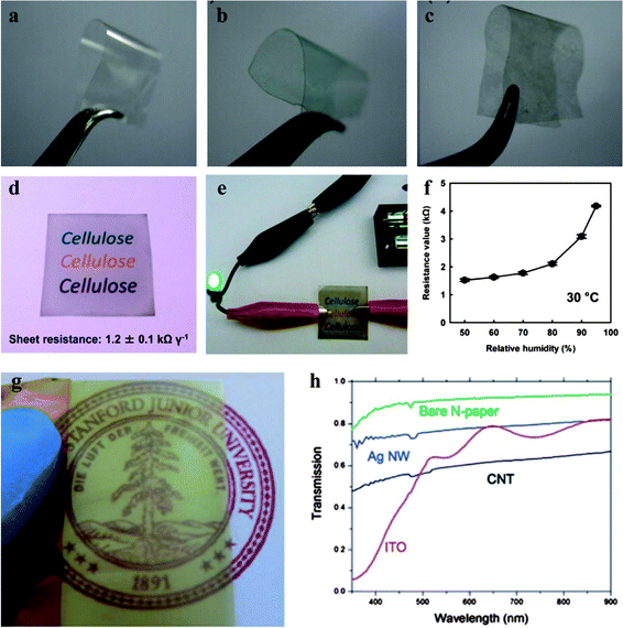
Functionalizing transparent paper substrates is required to process certain properties in electronic device applications. Introducing electrical conductivity to transparent paper is important for any optoelectronic device since both the light transmission through the surface and electron transport along the surface is required. As shown in Fig. 9, one method to make transparent and conductive paper is layer-by-layer technique to deposit conductive materials on transparent paper. Fig. 9(a)–(c) show digital images of transparent NFC paper, NFC/[Cu2+/GO (graphene oxide)]20 paper, and NFC/[RGO (reduced graphene oxide)]20 paper, respectively.120 The obtained flexible transparent conductive NFC film exhibits a transmittance of approximately 76% at 550 nm with a sheet resistance of 25 KΩ while illustrating a slight decrease in tensile strength from 153 MPa to 136 MPa after twenty circles of LBL assembly. Using NFC as a dispersing and reinforcing agent of carbon nanotube (CNT) is another promising approach to produce strong, ultrathin, flexible, and conductive films. The transparent and conductive CNT/TOCN (TEMPO oxidized cellulose nanofiber) film deposited on the PET is illustrated in Fig. 9(d), and an LED light illuminated by integrating the CNT/TOCN deposited PET with a connected electrical circuit is also displayed (Fig. 9(e)). As shown in Fig. 9(f), the sheet resistance of CNT/TOCN casted film changes with an increase of relative humidity, which is evidence for its potential application in humidity sensors.121 Another method is to over-coat the surface of transparent paper with an ultrathin layer of conductive material by solution based deposition or printing.49Fig. 9(g) shows a highly conductive and transparent paper over-coated with conductive ITO with a sputtering method. Solution based printing of conductive CNTs or Ag nanowires (NWs) can be applied. The optical transparency data before and after various conductive coatings is shown in Fig. 9(h). Note that the sheet resistance is 12 Ω sq−1 for ITO, 25 Ω sq−1 for AgNWs, and 200 Ω sq−1 for CNT. The highly conductive and transparent paper substrates are building blocks for future optoelectronic devices.
 |
| | Fig. 9 Images of (a) CNFs, (b) CNFs/[Cu2+/GO]20, (c) CNFs/[RGO]20. (d) Images of CNT/TOCN coated PET with a sheet resistance of 1.2 KΩ sq−1. (e) Transparent and conductive CNT/TOCN coated PET used to light a LED. (f) Resistance of CNT/TOCN coated PET vs. relative humidity. (g) Digital picture of ITO deposited nanopaper with a sheet resistance of 12 KΩ sq−1. (h) Total optical transmittance of bare nanopaper, and conductive paper deposited with CNT, Ag NWs, and ITO, respectively. | |
Vacuum based depositions such as metal sputtering were used to produce highly conductive channels on the nanopaper. This can be done without heat processing; therefore it will not affect the original properties of paper, such as shape stability, surface roughness, or paper appearance. Fig. 10(a) and (b) show a uniform sputtered gold line on the nanopaper, 1 mm in width and 40 mm in length, exhibiting a resistance of 34 Ω after sputtering for 5 min.107 Various printing methods have been developed for flexible electronics on plastic and paper substrates, such as inkjet printing, gravure coating, slot-die, curtain coating, Meyer rod coating, etc.122 These coating methods have different requirements for ink rheology, substrate parameters, substrate-ink interactions, and drying mechanisms. Inkjet printing is a promising approach to produce patterns on transparent paper with silver nanoparticles or nanowire inks commonly used as the conductive coating. Fig. 10(c) illustrates an antenna array on the nanostructure paper formed by inkjet printing silver nanoparticles.123 A silver nanoparticle printed grid pattern with a line width of 40 μm is also shown in Fig. 10(d). A single printed silver nanoparticle layer leads to a sheet resistance of 330 Ω sq−1 for a 25 mm2 area grid. As we can see from Fig. 10(e) and (f), the silver nanoparticle line has high printing resolution that is beneficial for fabricating electronic devices.123
 |
| | Fig. 10 (a) and (b) photos of gold sputtered line on nanopaper. (c) Antenna pattern on nanostructured paper formed by an inkjet printer using silver nanoparticles. (d) Digital image of an inkjet-printed silver nanoparticle grid on nanostructured paper, (e) and (f) are the amplified SEM images of inkjet-printed grid on nanostructured paper.107,123 | |
6. Devices based on transparent paper
6.1 Thin film transistors
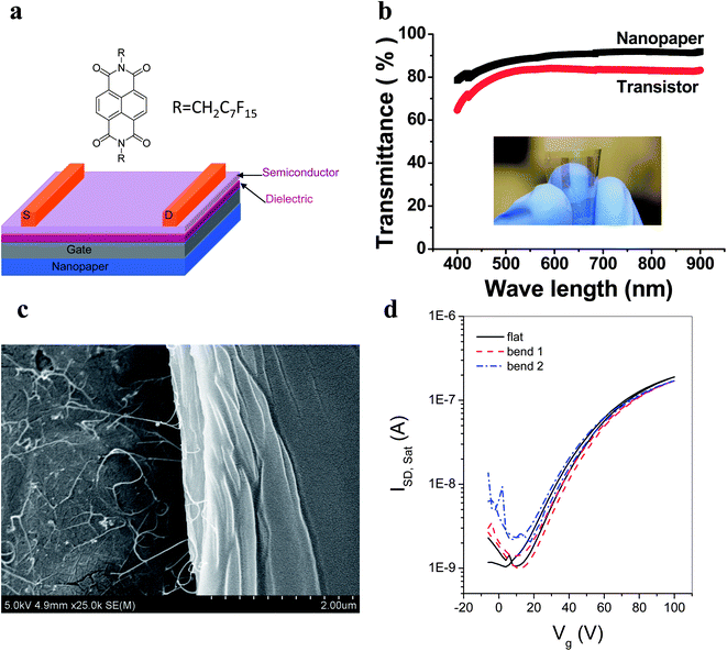
TFTs are key components for macroelectronics. Paper has been explored for building TFTs, either as a low-cost and printable substrate, or as a porous dielectric using liquid or gel-electrolyte gating.16,124–126 When used as a substrate, a thin layer coating is usually used to smooth out the surface due to the large surface roughness of the original surface; however such a coating layer will decrease the flexibility, bendability, and printability of paper substrate. When used as the porous dielectrics, the large thickness leads to a large gate voltage to achieve a reasonable on/off ratio. TFTs were recently demonstrated on transparent paper with a smooth surface roughness. As shown in Fig. 11(a), transparent nanopaper was used as a substrate without the need for any surface coating due to the nanoscale surface roughness, which made it compatible with the typical TFTs device structures. Transparent and conductive CNT films were printed as the transparent gate. Transparent N-type NTCDI-F15 was used as the semiconductor, and Al2O3 by atomic-layer-deposition (ALD) was used as the dielectric. As shown in Fig. 11(b) and its inset, the entire device is highly transparent, with a total transmittance up to 80%. Due to the numerous van de Waals forces and hydrogen bonds between functionalized CNTs and NFC fibers, CNT films sticks to the nanopaper surface well without probing through the dielectric layer, Fig. 11(c). The dielectric layer can be replaced by solution-based polymers, which may lead to all-printed paper transistors with fast, roll-to-roll processes. The entire device is highly flexible, as shown in Fig. 11(d). The transfer curves do not change significantly upon bending in different directions. We can envision that even foldable origami electronics is possible with these transparent substrates, which is impossible for plastic and other substrates.
 |
| | Fig. 11 (a) Schematic of the flexible transparent transistor structure on nanopaper. (b) Transmittance of nanopaper and transistor device with inserted picture of device. (c) SEM image of CNT layer under PMMA. (d) I–V curve before and after bending.45 | |
6.2 Organic-light-emitting diode
OLED devices are currently commercially available for displays and lighting. These devices are promising because they are thin, light-weight, and energy efficient compared to other devices such as liquid-crystal displays (LCDs). Flexible OLEDs are ubiquitously made on plastic substrates that are thin, smooth, optically clear, and have excellent barrier properties to oxygen and water. Transparent paper has nanoscale smoothness and its optical properties can be tuned from optically clear to optically hazy, which is beneficial for flexible OLED devices for different applications.48,50,53,127 OLEDs on transparent paper with high haze will have a wide angular light distribution for lighting, while OLEDs on paper with low haze will have a high clarity for in-door displays. Zhu et al. recently illustrated an OLED device on transparent nanopaper and the schematic structure is shown in Fig. 12(a). The transparent conductor is a thin layer of CNT, the hole injection layer is 10 nm molybdenum oxide (MoO3) and 30 nm PEDOT:PSS (poly(3,4-ethylenedioxythiophene):poly(styrenesulfonate)), the light emitting layer is green polyfluorene, and electron injection layer is 20 nm calcium. Note that each layer is less than 100 nm thick. Fig. 12(b) demonstrates a working OLED device that can be bent into an arch with a 1.5 mm curvature. There is no change in the I–V curve for the flexible nanopaper OLED before and after bending (Fig. 12(c)); however, the efficiency is low and the lighting uniformity is poor for the proof-of-concept devices. This may be due to the large series resistance in the transparent conductor layer, or the non-uniformity of the nanopaper after the device fabrication, which is primarily due to the shape instability of transparent paper. The shape stability of transparent paper needs to improve as the fabrication processes involve solvents which can swell the NFC fibers.
 |
| | Fig. 12 (a) Schematic of flexible OLED on transparent nanopaper substrate. From top to bottom, the device consists of a cathode aluminum layer, a 20 nm calcium electron injection layer, a light emitting layer of green polyfluorene, a 10 nm molybdenum oxide (MoO3) and 30 nm PEDOT:PSS (poly(3,4-ethylenedioxythiophene):poly(styrenesulfonate)) hole injection layer, and a layer of CNT coated on nanopaper. (b) Image of a functioning nanopaper OLED. (c) I–V curve before and after bending.53 | |
6.3 Organic photovoltaic devices
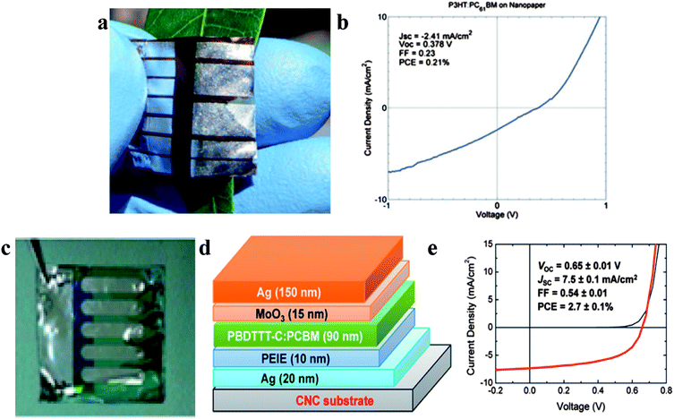
The high optical haze of transparent paper makes it extremely attractive for high-performance organic solar cells with advanced light management, in addition to the advantages of being printable. As discussed in the part of optical properties, the optical properties of transparent paper can be modulated with different structures. Transparent paper can have an optical haze up to 60%, which means the majority of the transmitted light is scattered off the normal direction as opposed to plastic substrates that display low optical haze (<1%). Substantial light scattering leads to an increase of the optical path length in the active layer, even total reflection, which results in a large increase in the optical absorption. Light scattering is an intrinsic property to the paper substrate that can eliminate additional light management mechanisms in thin film solar cells. Organic solar cells on paper substrates have been demonstrated either through a lamination or surface treatment of regular paper.12,20,49,55,128 Organic solar cell on transparent paper substrates were recently demonstrated, as shown in Fig. 13. Hu et al. demonstrated that organic solar cells with regioregular poly(3-hexylthiophene) (P3HT, Rieke, EE-grade):[6,6]-phenyl-C61-butyric acid methyl ester (PCBM, Nano-C) and poly(3,4-ethylenedioxythiophene):poly(styrene sulfonate) (PEDOT:PSS, Clevios P VP AI 4083) materials, with an energy conversion efficiency of 0.21%. From the current–voltage output, the series resistance is high, which may be due to the large interface resistance and the high resistance of transparent electrode layer. There is limited shunt resistance, which may be due to the possible shorting inside the device. In a separate study, Zhou et al. demonstrated an OPV device on transparent paper with a higher efficiency (∼2.7%). The finished device and device structure are shown in Fig. 13(a) and (b), respectively. The I–V curve of device with and without illumination shows excellent rectification behavior, indicating a smaller series resistance and a large shunt resistance. It is anticipated that upon further improved engineering the efficiency of thin film OPVs on transparent paper will be higher than if they were hosted on plastic substrate due to the light scattering properties (Table 2).
 |
| | Fig. 13 (a) Images of solar cells based on transparent paper. (b) The I–V curve of solar cell fabricated on transparent paper. (c) Digital image of CNC based solar cell. (d) Schematic structure of solar cell. (e) I–V curve of CNC based solar cell.49,55 | |
Table 2 Organic solar cells on paper substrate
| Substrate for OPV |
Substrate transmittance |
Substrate haze |
Energy conversion efficiency |
Lifetime |
Ref. |
| Plastic substrate |
∼90% |
∼1–3% |
∼11% |
NA |
129
|
| Regular paper |
<50% |
70–80% |
∼1.4% |
>500 h |
12
|
| Nanopaper |
85% |
10–20% |
∼0.2%, ∼2.7% |
NA |
49 and 55
|
6.4 Printed foldable antenna
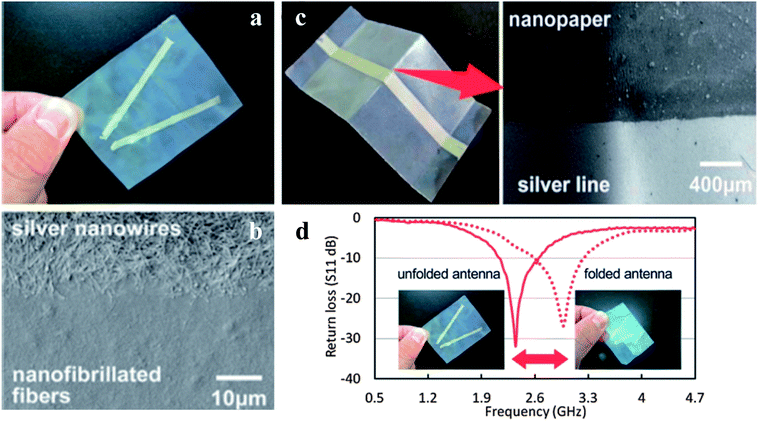
An antenna is an important part of a satellite, computer, or other RFID based devices to transmit and receive signals. Foldable antennas are especially highly desirable for small sized devices. Paper has been demonstrated by several groups as a substrate to host antennas due to their foldability, printability, light-weight, and low-cost.3,23,44,130–133 The drawback of regular paper based antennas is high return loss caused by the rough surface. Coating has been used to form a smoother paper surface, but the foldability decreases due to the easily cracked coating layer.134 Nanopaper with a nanoscale surface smoothness was used as a substrate for antenna by Nogi.44 As shown in Fig. 14(a) and (b), the antenna is made by screen-printing V-shaped silver nanowire lines on smooth surface nanopaper. The sharp printed silver ink edge is well defined, which shows the nanopaper has good printability for nano-functional ink. The distinct 3D network of nanopaper make it durable even when folded, as demonstrated by the smooth, continuous surface of silver nanowire lines in Fig. 14(c) and the sustained sensitivity of the antenna in Fig. 14(d). The return loss of nanopaper antennas is much lower than the antennas on regular paper due to the smooth surface. Note that the resonance peak changes when folding, and then returns back after unfolding. This makes it capable for nanopaper antennas to transmit and receive multiple frequency band signals only by folding and unfolding.
 |
| | Fig. 14 (a) Return losses of nanopaper based antennas before (solid line) and after folding (dotted line). (b) Silver line printed on nanopaper. (c) Images of silver printed nanopaper after folding. (d) SEM image of sliver printed line.44 | |
6.5 Resistive paper touch screens
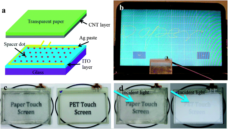
Integrating transparent paper with conductive materials (such as CNT, graphene, Ag NWs/particles, ITO) demonstrates an extensive range of applications in transparent flexible devices.49,120 Transparent paper with a large optical haze value is ideal for eliminating strong light reflection causing glare when it exposed to sunlight.67,135 A four-wire resistive touch screen device was demonstrated recently with transparent and hazy hybrid paper.54 The device was then assembled using CNT coated hybrid nanostructures. The four-wire touch screen can sense the physical touch and transfer signals in a display device. The contact made by touching the screen surface creates a voltage divider when the two conductive layers are in contact at that point, which pinpoints the Y-coordinate from the voltage reading by the X-electrodes. The process repeats with the X-coordinate being taken from one of the Y-electrodes, and the 2D position of this contact can be identified by the controller circuit. The structure of paper touch screen is displayed in Fig. 15(a), the CNT-coated transparent hybrid paper was used to substitute conductive PET as the top electrode of the touch screen. The word “paper” was successfully displayed on the screen of computer when the pattern was written on the paper touch screen by a stylus pen (Fig. 15(b)). Fig. 5(c) shows the paper touch screen (left) and PET touch screen (right), and that the underneath pattern of both screen are clear. When they are exposed to sunlight as showed in Fig. 15(d), the pattern under the PET touch screen is invisible, but the paper touch screen demonstrates high anti-glaring characteristics, which is important for outdoors applications.
 |
| | Fig. 15 (a) Schematic structure of a four-wire touch screen with transparent and conductive paper. (b) The word “paper” was displayed in the screen by stimulating an assembled paper touch. (c) Left: a paper touch screen, right: a PET touch screen. (d) Two types of touch screen exposed to sunlight: a paper touch screen without glare (left) and a PET touch screen with great glare (right). All pictures were taken at a similar angle.54 | |
7. Discussion and future prospects
Transparent paper can potentially replace plastic for printed green electronics just as plastic has replaced glass for flexible electronics. Universities, governmental labs, and industries have shown increasing interest in transparent paper for next-generation green electronics. Recently progress includes: (1) various types of transparent paper demonstrated a continuous decrease in energy and time consuming for fabrication; (2) good understanding of fundamental properties and processing compatibilities of the substrates with various inks or vacuum related processes; (3) demonstrations of proof-of-concept devices with excellent mechanical flexibility, and even bendability. It is very likely that new types of devices will be demonstrated with much improved performances, and system integrations such as electronics systems on transparent paper can be potentially developed. Ideally, functional flexible electronics systems can be fabricated on transparent paper with the current roll-to-roll fabrication speed (up to 2000 ft min−1) and with the similar, or even better, performance on plastic substrates. However, there are tremendous challenges, including the follow: (1) transparent paper nanofabrication challenges, with an aim of much higher speed and much lower energy consumption; (2) substrate property improvement including the shape stability, water absorption, and barrier properties to water and oxygen; (3) printing process development and improved properties of printed materials; and (4) device fabrication, reliability and integrations with roll-to-roll processing. Regarding fabrication of transparent paper with a high speed and low cost, new processes for disintegrating fiber down to NFCs and fabricating papers need to be developed. Substrate properties need to match that of plastics for a viable replacement. It is possible that infiltration of porous transparent paper with polymers is a possible route to improve properties such as barrier resistance to oxygen and water, shape stability and increase the clarity for displays. Understanding the surface properties and paper substrate-ink interaction is critical for developing printing processes for high-speed roll-to-roll coating. For device applications, it is very likely that the transparent paper will give us more flexibility to tune the substrate properties for different applications. One example is that the optical transmission haze is highly tunable, which allow advanced light management for displays, lighting and solar cells.
Acknowledgements
We acknowledge the support from DOD (Air Force of Scientific Research) Young Investigator Program (FA95501310143). Z.F. would like to thank the China Scholarship Council (CSC) for financial support.
Notes and references
- D. Tobjörk and R. Österbacka, Adv. Mater., 2011, 23, 1935–1961 CrossRef PubMed.
-
P. Barquinha, R. Martins, L. Pereira and E. Fortunato, Transparent Oxide Electronics: From Materials to Devices, John Wiley & Sons Ltd, New York, 2012, pp. 211–266 Search PubMed.
- A. Russo, B. Y. Ahn, J. J. Adams, E. B. Duoss, J. T. Bernhard and J. A. Lewis, Adv. Mater., 2011, 23, 3426–3430 CrossRef CAS PubMed.
- A. C. Siegel, S. T. Phillips, M. D. Dickey, N. Lu, Z. Suo and G. M. Whitesides, Adv. Funct. Mater., 2010, 20, 28–35 CrossRef CAS.
- C. Yang, H. Gu, W. Lin, M. M. Yuen, C. P. Wong, M. Xiong and B. Gao, Adv. Mater., 2011, 23, 3052–3056 CrossRef CAS PubMed.
- P. Ihalainen, A. Maattanen, J. Jarnstrom, D. Tobjork, R. Osterbacka and J. Peltonen, Ind. Eng. Chem. Res., 2012, 51, 6025–6036 CrossRef CAS.
- D. H. Kim, Y. S. Kim, J. Wu, Z. J. Liu, J. Z. Song, H. S. Kim, Y. G. Y. Huang, K. C. Hwang and J. A. Rogers, Adv. Mater., 2009, 21, 3703–3707 CrossRef CAS.
- R. Bollström, A. Määttänen, D. Tobjörk, P. Ihalainen, N. Kaihovirta, R. Österbacka, J. Peltonen and M. Toivakka, Org. Electron., 2009, 10, 1020–1023 CrossRef.
- B. Trnovec, M. Stanel, U. Hahn, A. C. Hübler, H. Kempa, R. Sangl and M. Forster, Prof. Papermaking, 2009, 6, 48–51 Search PubMed.
- P. Ihalainen, A. Määttänen, J. Järnström, D. Tobjörk, R. Österbacka and J. Peltonen, Ind. Eng. Chem. Res., 2012, 51, 6025–6036 CrossRef CAS.
- T. Öhlund, J. Örtegren, S. Forsberg and H.-E. Nilsson, Appl. Surf. Sci., 2012, 259, 731–739 CrossRef.
- M. C. Barr, J. A. Rowehl, R. R. Lunt, J. Xu, A. Wang, C. M. Boyce, S. G. Im, V. Bulović and K. K. Gleason, Adv. Mater., 2011, 23, 3500–3505 CrossRef CAS PubMed.
- D. Y. Kim and A. J. Steckl, ACS Appl. Mater. Interfaces, 2010, 2, 3318–3323 CAS.
- L. Hu, H. Wu, F. La Mantia, Y. Yang and Y. Cui, ACS Nano, 2010, 4, 5843–5848 CrossRef CAS PubMed.
-
E. Fortunato, N. Correia, P. Barquinha, C. Costa, L. Pereira, G. Gonçalves and R. Martins, International Society for Optics and Photonics, 2009, 217, p. 72170K-1-11 Search PubMed.
- R. Martins, P. Barquinha, L. Pereira, N. Correia, G. Goncalves, I. Ferreira and E. Fortunato, Appl. Phys. Lett., 2008, 93, 203501–203503 CrossRef.
- J. Jiang, J. Sun, W. Dou, B. Zhou and Q. Wan, Appl. Phys. Lett., 2011, 98, 113507–113507 CrossRef.
-
D. Tobjörk, PhD Thesis, Print Low-voltage Transistors on Plastic and Paper, Åbo Akademi University, Finland, 2012 Search PubMed.
- B. Lamprecht, R. Thünauer, M. Ostermann, G. Jakopic and G. Leising, Phys. Status Solidi A, 2005, 202, R50–R52 CrossRef CAS.
- F. Wang, Z. Chen, L. Xiao, B. Qu and Q. Gong, Sol. Energy Mater. Sol. Cells, 2010, 94, 1270–1274 CrossRef CAS.
- T. S. Kim, S. I. Na, S. S. Kim, B. K. Yu, J. S. Yeo and D. Y. Kim, Phys. Status Solidi RRL, 2012, 6, 13–15 CrossRef CAS.
- B. Wang and L. L. Kerr, Sol. Energy Mater. Sol. Cells, 2011, 95, 2531–2535 CrossRef CAS.
- V. Lakafosis, A. Rida, R. Vyas, L. Yang, S. Nikolaou and M. M. Tentzeris, Proc. IEEE, 2010, 98, 1601–1609 CrossRef.
- W. Dungchai, O. Chailapakul and C. S. Henry, Analyst, 2011, 136, 77–82 RSC.
- J. W. Han, B. Kim, J. Li and M. Meyyappan, J. Phys. Chem. C, 2012, 116, 22094–22097 CAS.
- H. Yano, J. Sugiyama, A. N. Nakagaito, M. Nogi, T. Matsuura, M. Hikita and K. Handa, Adv. Mater., 2005, 17, 153–155 CrossRef CAS.
- S. Iwamoto, A. N. Nakagaito, H. Yano and M. Nogi, Appl. Phys. A: Mater. Sci. Process., 2005, 81, 1109–1112 CrossRef CAS.
- Q. Yang, H. Fukuzumi, T. Saito, A. Isogai and L. Zhang, Biomacromolecules, 2011, 12, 2766–2771 CrossRef CAS PubMed.
- S. Liu and L. Zhang, Cellulose, 2009, 16, 189–198 CrossRef CAS.
- H. S. Qi, C. Y. Chang and L. Zhang, Green Chem., 2009, 11, 177–184 RSC.
- Q. L. Yang, X. Z. Qin and L. N. Zhang, Cellulose, 2011, 18, 681–688 CrossRef CAS.
- Q. Yang, H. Qi, A. Lue, K. Hu, G. Cheng and L. Zhang, Carbohydr. Polym., 2011, 83, 1185–1191 CrossRef CAS.
- L. Zhang, D. Ruan and J. Zhou, Ind. Eng. Chem. Res., 2001, 40, 5923–5928 CrossRef CAS.
- S. C. M. Fernandes, L. Oliveira, C. S. R. Freire, A. J. D. Silvestre, C. P. Neto, A. Gandini and J. Desbrieres, Green Chem., 2009, 11, 2023–2029 RSC.
- M. Österberg, J. Vartiainen, J. Lucenius, U. Hippi, J. Seppälä, R. Serimaa and J. Laine, ACS Appl. Mater. Interfaces, 2013, 5, 4640–4647 Search PubMed.
- H. Sehaqui, A. D. Liu, Q. Zhou and L. A. Berglund, Biomacromolecules, 2010, 11, 2195–2198 CrossRef CAS PubMed.
- S. Varanasi and W. J. Batchelor, Cellulose, 2013, 20, 211–215 CrossRef CAS.
- K. L. Spence, R. A. Venditti, O. J. Rojas, J. J. Pawlak and M. A. Hubbe, Bioresources, 2011, 6, 4370–4388 CAS.
- M. Nogi, S. Iwamoto, A. N. Nakagaito and H. Yano, Adv. Mater., 2009, 21, 1595–1598 CrossRef CAS.
- M. Nogi and H. Yano, Appl. Phys. Lett., 2009, 94, 233117 CrossRef.
- H. Fukuzumi, T. Saito, T. Iwata, Y. Kumamoto and A. Isogai, Biomacromolecules, 2008, 10, 162–165 CrossRef PubMed.
- M. I. Shams, M. Nogi, L. A. Berglund and H. Yano, Soft Matter, 2012, 8, 1369–1373 RSC.
-
N. Komoda, M. Nogi, K. Suganuma, H. Koga and K. Otsuka, in Nanotechnology (IEEE-NANO) 12th IEEE Conference on 2012, 2012, 1–5 Search PubMed.
- M. Nogi, N. Komoda, K. Otsuka and K. Suganuma, Nanoscale, 2013, 5, 4395–4399 RSC.
- J. Huang, H. Zhu, Y. Chen, C. Preston, K. Rohrbach, J. Cumings and L. Hu, ACS Nano, 2013, 7, 2106–2113 CrossRef CAS PubMed.
- A. N. Nakagaito, M. Nogi and H. Yano, MRS Bull., 2010, 35, 214–218 CrossRef CAS.
- M. Nogi and H. Yano, Adv. Mater., 2008, 20, 1849–1852 CrossRef CAS.
- Y. Okahisa, A. Yoshida, S. Miyaguchi and H. Yano, Compos. Sci. Technol., 2009, 69, 1958–1961 CrossRef CAS.
- L. B. Hu, G. Y. Zheng, J. Yao, N. A. Liu, B. Weil, M. Eskilsson, E. Karabulut, Z. C. Ruan, S. H. Fan, J. T. Bloking, M. D. McGehee, L. Wagberg and Y. Cui, Energy Environm. Sci., 2013, 6, 513–518 RSC.
- S. Ummartyotin, J. Juntaro, M. Sain and H. Manuspiya, Ind. Crops Prod., 2012, 35, 92–97 CrossRef CAS.
- W. Zhang, X. Zhang, C. Lu, Y. Wang and Y. Deng, J. Phys. Chem. C, 2012, 116, 9227–9234 CAS.
- L. Hu, N. Liu, M. Eskilsson, G. Zheng, J. McDonough, L. Wågberg and Y. Cui, Nano Energy, 2013, 2, 138–145 CrossRef CAS.
- H. Zhu, Z. Xiao, D. Liu, Y. Li, N. J. Weadock, Z. Fang, J. Huang and L. Hu, Energy Environm. Sci., 2013, 6, 2105–2111 RSC.
- Z. Fang, H. Zhu, C. Preston, X. Han, Y. Li, S. Lee, X. Chai, G. Chen and L. Hu, J. Mater. Chem. C, 2013, 5, 4395–4399 Search PubMed.
- Y. Zhou, C. Fuentes-Hernandez, T. M. Khan, J.-C. Liu, J. Hsu, J. W. Shim, A. Dindar, J. P. Youngblood, R. J. Moon and B. Kippelen, Sci. Rep., 2013, 3, 1536–1541 Search PubMed.
-
D. N. S. Hon and N. Shiraishi, Wood and Cellulosic Chemistry, CRC Press, 2000 Search PubMed.
- H. Zhu, Z. Jia, Y. Chen, N. Weadock, J. Wan, O. Vaaland, X. Han, T. Li and L. Hu, Nano Lett., 2013, 13, 3093–3100 CrossRef CAS PubMed.
- G. Zheng, Y. Cui, E. Karabulut, L. Wågberg, H. Zhu and L. Hu, MRS Bull., 2013, 38, 320–325 CrossRef CAS.
- D. Klemm, F. Kramer, S. Moritz, T. Lindstrom, M. Ankerfors, D. Gray and A. Dorris, Angew. Chem., Int. Ed., 2011, 50, 5438–5466 CrossRef CAS PubMed.
-
F. W. Herrick, R. L. Casebier, J. K. Hamilton and K. R. Sandberg, Microfibrillated cellulose, a new cellulose product: properties, uses and commercial potential, ITT Rayonier Inc., Shelton, WA, 1983 Search PubMed.
- G. Chinga-Carrasco, Nanoscale Res. Lett., 2011, 6, 1–7 CrossRef PubMed.
- Z. Gui, H. Zhu, E. Gillette, X. Han, G. W. Rubloff, L. Hu and S. B. Lee, ACS Nano, 2013, 7, 6037–6046 CrossRef CAS PubMed.
- X. Chen, H. Zhu, C. Liu, Y.-C. Chen, N. Weadock, G. Rubloff and L. Hu, J. Mater. Chem. A, 2013, 1, 8201–8208 CAS.
- A. N. J. Heyn, J. Ultrastruct. Res., 1969, 26, 52–68 CrossRef CAS PubMed.
- D. Klemm, B. Heublein, H.-P. Fink and A. Bohn, Angew. Chem., Int. Ed., 2005, 44, 3358–3393 CrossRef CAS PubMed.
- D. Klemm, F. Kramer, S. Moritz, T. Lindström, M. Ankerfors, D. Gray and A. Dorris, Angew. Chem., Int. Ed., 2011, 50, 5438–5466 CrossRef CAS PubMed.
- H. Zhu, S. Parvinian, C. Preston, O. Vaaland, Z. Ruan and L. Hu, Nanoscale, 2013, 5, 3787–3792 RSC.
- P. B. Filson, B. E. Dawson-Andoh and D. Schwegler-Berry, Green Chem., 2009, 11, 1808–1814 RSC.
- A. Isogai, T. Saito and H. Fukuzumi, Nanoscale, 2011, 3, 71–85 RSC.
-
A. F. Turbak, F. W. Snyder and K. R. Sandberg, Microfibrillated Cellulose—A New Composition of Commercial Significance, ITT Rayonier Inc., Shelton, WA Search PubMed.
- T. Saito, S. Kimura, Y. Nishiyama and A. Isogai, Biomacromolecules, 2007, 8, 2485–2491 CrossRef CAS PubMed.
- M. Henriksson, G. Henriksson, L. A. Berglund and T. Lindstrom, Eur. Polym. J., 2007, 43, 3434–3441 CrossRef CAS.
- T. Saito, Y. Nishiyama, J.-L. Putaux, M. Vignon and A. Isogai, Biomacromolecules, 2006, 7, 1687–1691 CrossRef CAS PubMed.
- T. Saito and A. Isogai, Carbohydr. Polym., 2005, 61, 183–190 CrossRef CAS.
- N. Lavoine, I. Desloges, A. Dufresne and J. Bras, Carbohydr. Polym., 2012, 90, 735–764 CrossRef CAS PubMed.
- H. L. Zhu, M. Helander, C. Moser, A. Stahlkranz, D. Soderberg, G. Henriksson and M. Lindstrom, Curr. Org. Chem., 2012, 16, 1871–1875 CrossRef CAS.
- K. Abe and H. Yano, Carbohydr. Polym., 2011, 85, 733–737 CrossRef CAS.
- K. Abe and H. Yano, Cellulose, 2012, 19, 1907–1912 CrossRef CAS.
- A. Nakayama, A. Kakugo, J. P. Gong, Y. Osada, M. Takai, T. Erata and S. Kawano, Adv. Funct. Mater., 2004, 14, 1124–1128 CrossRef CAS.
- R. J. Moon, A. Martini, J. Nairn, J. Simonsen and J. Youngblood, Chem. Soc. Rev., 2011, 40, 3941–3994 RSC.
- R. R. Lahiji, X. Xu, R. Reifenberger, A. Raman, A. Rudie and R. J. Moon, Langmuir, 2010, 26, 4480–4488 CrossRef CAS PubMed.
- D. v. d. Reyden, C. Hofmann and M. Baker, J. Am. Inst. Conserv., 1993, 32, 177–206 CrossRef.
-
K. Bachmann, The Book and Paper Annual, 1983, vol. 2, 3–13 Search PubMed.
-
T. Koike and M. Amano, Google Patents, 4137046, 1979.
-
W. J. Castle and R. Mehta, Google Patents, US669281981, 2004.
-
D. R. Simcoke, Google Patents, WO1991001882A1, 1991.
- T. Nishino and N. Arimoto, Biomacromolecules, 2007, 8, 2712–2716 CrossRef CAS PubMed.
- T. Nishino, I. Matsuda and K. Hirao, Macromolecules, 2004, 37, 7683–7687 CrossRef CAS.
- M. I. Shams, S. Ifuku, M. Nogi, T. Oku and H. Yano, Appl. Phys. A: Mater. Sci. Process., 2011, 102, 325–331 CrossRef CAS.
- S. C. M. Fernandes, C. S. R. Freire, A. J. D. Silvestre, C. P. Neto, A. Gandini, L. A. Berglund and L. Salmen, Carbohydr. Polym., 2010, 81, 394–401 CrossRef CAS.
- H. Yang, A. Tejado, N. Alam, M. Antal and T. G. M. van de Ven, Langmuir, 2012, 28, 7834–7842 CrossRef CAS PubMed.
- C. F. Cross, E. T. Bevan and C. Beadle, Ber. Dtsch. Chem. Ges., 1893, 26, 1090–1097 CrossRef.
- H. P. Fink, P. Weigel, H. J. Purz and J. Ganster, Prog. Polym. Sci., 2001, 26, 1473–1524 CrossRef CAS.
- M. B. Turner, S. K. Spear, J. D. Holbrey and R. D. Rogers, Biomacromolecules, 2004, 5, 1379–1384 CrossRef CAS PubMed.
-
A. F. Turbak, F. W. Snyder and K. R. Sandberg, Google Patents, CA11499219A1, 1983.
- T. Taniguchi and K. Okamura, Polym. Int., 1998, 47, 291–294 CrossRef CAS.
- M. Henriksson, L. A. Berglund, P. Isaksson, T. Lindstrom and T. Nishino, Biomacromolecules, 2008, 9, 1579–1585 CrossRef CAS PubMed.
- I. Siró, D. Plackett, M. Hedenqvist, M. Ankerfors and T. Lindström, J. Appl. Polym. Sci., 2011, 119, 2652–2660 CrossRef.
- Q. Wang, J. Y. Zhu and J. M. Considine, ACS Appl. Mater. Interfaces, 2013, 5, 2527–2534 CAS.
- H. Yano, J. Sugiyama, A. N. Nakagaito, M. Nogi, T. Matsuura, M. Hikita and K. Handa, Adv. Mater., 2005, 17, 153–155 CrossRef CAS.
- M. Nogi, K. Handa, A. N. Nakagaito and H. Yano, Appl. Phys. Lett., 2005, 87, 243110 CrossRef.
- S. Iwamoto, A. N. Nakagaito, H. Yano and M. Nogi, Appl. Phys. A: Mater. Sci. Process., 2005, 81, 1109–1112 CrossRef CAS.
- H. Liu, D. Liu, F. Yao and Q. Wu, Bioresour. Technol., 2010, 101, 5685–5692 CrossRef CAS PubMed.
- S. Ifuku, A. Ikuta, T. Hosomi, S. Kanaya, Z. Shervani, M. Morimoto and H. Saimoto, Carbohydr. Polym., 2012, 89, 865–869 CrossRef CAS PubMed.
-
C. F. Bohren and D. R. Huffman, Absorption and scattering of light by small particles, Wiley.com, 2008 Search PubMed.
- C. Preston, Z. Fang, J. Murray, H. Zhu, J. Dai, J. N. Munday and L. Hu, J. Mater. Chem. C, 2014 10.1039/c3tc31726a.
- M. C. Hsieh, C. Kim, M. Nogi and K. Suganuma, Nanoscale, 2013, 5, 9289–9295 RSC.
- H. Sehaqui, M. Allais, Q. Zhou and L. A. Berglund, Compos. Sci. Technol., 2011, 71, 382–387 CrossRef CAS.
- M. Nogi, C. Kim, T. Sugahara, T. Inui, T. Takahashi and K. Suganuma, Appl. Phys. Lett., 2013, 102, 181911 CrossRef.
- S. Soares, G. Camino and S. Levchik, Polym. Degrad. Stab., 1995, 49, 275–283 CrossRef CAS.
- J. B. Dahiya and K. Kumar, J. Sci. Ind. Res., 2009, 68, 548–554 CAS.
- H. Fukuzumi, T. Saito, Y. Okita and A. Isogai, Polym. Degrad. Stab., 2010, 95, 1502–1508 CrossRef CAS.
- Y. Okahisa, A. Yoshida, S. Miyaguchi and H. Yano, Compos. Sci. Technol., 2009, 69, 1958–1961 CrossRef CAS.
- H. Fukuzumi, T. Saito, T. Wata, Y. Kumamoto and A. Isogai, Biomacromolecules, 2009, 10, 162–165 CrossRef CAS PubMed.
- A. W. Martinez, S. T. Phillips, G. M. Whitesides and E. Carrilho, Anal. Chem., 2009, 82, 3–10 CrossRef PubMed.
- X. Li, J. Tian, T. Nguyen and W. Shen, Anal. Chem., 2008, 80, 9131–9134 CrossRef CAS PubMed.
- A. K. Yetisen, M. S. Akram and C. R. Lowe, Lab Chip, 2013, 13, 2210–2251 RSC.
- A. W. Martinez, S. T. Phillips, M. J. Butte and G. M. Whitesides, Angew. Chem., Int. Ed., 2007, 46, 1318–1320 CrossRef CAS PubMed.
- H. Sehaqui, Q. Zhou, O. Ikkala and L. A. Berglund, Biomacromolecules, 2011, 12, 3638–3644 CrossRef CAS PubMed.
- K. Gao, Z. Shao, X. Wu, X. Wang, J. Li, Y. Zhang, W. Wang and F. Wang, Carbohydr. Polym., 2013, 97, 243–251 CrossRef CAS PubMed.
- H. Koga, T. Saito, T. Kitaoka, M. Nogi, K. Suganuma and A. Isogai, Biomacromolecules, 2013, 14, 1160–1165 CrossRef CAS PubMed.
-
A. A. Tracton, Coatings technnology handbook, CRC Press, 2005 Search PubMed.
- T. T. Nge, M. Nogi and K. Suganuma, J. Mater. Chem. C, 2013, 1, 5235–5243 RSC.
- P. Andersson, D. Nilsson, P. O. Svensson, M. Chen, A. Malmström, T. Remonen, T. Kugler and M. Berggren, Adv. Mater., 2002, 14, 1460–1464 CrossRef CAS.
- F. Eder, H. Klauk, M. Halik, U. Zschieschang, G. Schmid and C. Dehm, Appl. Phys. Lett., 2004, 84, 2673–2675 CrossRef CAS.
- Y. H. Kim, D. G. Moon and J. I. Han, IEEE Electron Device Lett., 2004, 25, 702–704 CrossRef CAS.
- S. H. Min, C. K. Kim, H. N. Lee and D. G. Moon, Mol. Cryst. Liq. Cryst., 2012, 563, 159–165 CrossRef CAS.
- T. S. Kim, S. I. Na, S. S. Kim, B. K. Yu, J. S. Yeo and D. Y. Kim, Phys. Status Solidi RRL, 2012, 6, 13–15 CrossRef CAS.
- R. E. Gains, Science, 2011, 332, 293 CrossRef PubMed.
- G. Orecchini, F. Alimenti, V. Palazzari, A. Rida, M. M. Tentzeris and L. Roselli, IET Microwaves Antennas & Propagation, 2011, 5, 993–1001 Search PubMed.
- A. Rida, L. Yang, R. Vyas and M. M. Tentzeris, IEEE Antenn. Propag. Mag., 2009, 51, 13–23 CrossRef.
- F. Alimenti, M. Virili, G. Orecchini, P. Mezzanotte, V. Palazzari, M. M. Tentzeris and L. Roselli, IEEE Trans. Microwave Theory Tech., 2011, 59, 627–637 CrossRef.
- D. E. Anagnostou, A. A. Gheethan, A. K. Amert and K. W. Whites, J. Disp. Technol., 2010, 6, 558–564 CrossRef CAS.
- L. Yang, A. Rida, R. Vyas and M. M. Tentzeris, IEEE Trans. Microwave Theory Tech., 2007, 55, 2894–2901 CrossRef.
- B. T. Liu, Y. T. Teng, R. H. Lee, W. C. Liaw and C. H. Hsieh, Colloids Surf., A, 2011, 389, 138–143 CrossRef CAS.
Footnote |
| † These authors contributed equally to the manuscript. |
|
| This journal is © The Royal Society of Chemistry 2014 |
Click here to see how this site uses Cookies. View our privacy policy here. ![[thin space (1/6-em)]](https://www.rsc.org/images/entities/char_2009.gif) 000.65 Natural cellulose is usually found in a mixture with random amorphous hemicellulose, and bio ‘glue’ lignin. Fig. 1(c) is the electron microscope image of the cross section of a spruce-fiber cell wall,59 from which the microfibrils are well defined. The hierarchical structure of wood fibers makes it possible to liberate the bio nanofiber from wood through disintegration process. NFC has many unique properties, such as excellent mechanical strength, interesting light scattering behavior, large specific surface area (100–200 g m−2), high aspect ratio (100–150), and active surface modification properties.60,66 Applying NFC to make transparent flexible electronics has attracted worldwide interest for its high transmittance, tunable optical properties, excellent flexibility, and light weight.67
000.65 Natural cellulose is usually found in a mixture with random amorphous hemicellulose, and bio ‘glue’ lignin. Fig. 1(c) is the electron microscope image of the cross section of a spruce-fiber cell wall,59 from which the microfibrils are well defined. The hierarchical structure of wood fibers makes it possible to liberate the bio nanofiber from wood through disintegration process. NFC has many unique properties, such as excellent mechanical strength, interesting light scattering behavior, large specific surface area (100–200 g m−2), high aspect ratio (100–150), and active surface modification properties.60,66 Applying NFC to make transparent flexible electronics has attracted worldwide interest for its high transmittance, tunable optical properties, excellent flexibility, and light weight.67

![[thin space (1/6-em)]](https://www.rsc.org/images/entities/char_2009.gif) 000 kW h per ton is a hurdle for the development and application of NFC in industry. Enzymatic pretreatment, chemical pretreatment, and refining have been applied in conjunction or as single stage treatments to break up the structure of the raw material, hence reducing the energy demand to produce NFC.71–75 Zhu et al. reported a novel energy-efficient method named “nanopulping” with an energy consumption at 443 kW h per t.76 The NFCs exhibit gel-like properties in water at low concentrations (1–2%) (Fig. 2(a)), hence the NFC is widely used to prepare hydrogels, aerogels, and thickeners in food.59,77–79 Due to the large presence of hydroxyl groups, the pristine nanocellulose tends to aggregate, especially when they are dried. Surface modification is employed, such as oxidation the hydroxyl group to carboxyl group via TEMPO treatment, to improve the stability and better dispersion. There are other cellulose nanofibers from plant, tunicate, bacterial, and algae that are not derived from wood.80 The bacterial cellulose is quite pure with a larger water content and longer chain length. Fig. 2(b) shows the electron microscope image of NFC with an average diameter of 30 nm (20–60 nm range) obtained by mechanical fibrillation from the hardwood sulfite pulps.44 The high aspect ratio along with the disordered amorphous region and ordered crystalline region in NFC grant the nanopaper with both excellent flexibility and high mechanical strength. The nanopaper made from NFC is widely used as a flexible transparent biodegradable substrate for advanced electronic and energy devices.45,49,53 The other important group of nanocellulose is the cellulose nanocrystal (CNC), which is isolated by hydrolyzing away the amorphous fraction and leaving the pure crystalline segments. Compared to the NFC, the CNC has higher crystallinity and a smaller aspect ratio. This gives CNC excellent mechanical properties that make it suitable for reinforcing materials in composite material, such as filler, plastic, and polymer. The flexibility of CNC is less than NFC, which limits the application of CNC as a substrate in flexible electronics.
000 kW h per ton is a hurdle for the development and application of NFC in industry. Enzymatic pretreatment, chemical pretreatment, and refining have been applied in conjunction or as single stage treatments to break up the structure of the raw material, hence reducing the energy demand to produce NFC.71–75 Zhu et al. reported a novel energy-efficient method named “nanopulping” with an energy consumption at 443 kW h per t.76 The NFCs exhibit gel-like properties in water at low concentrations (1–2%) (Fig. 2(a)), hence the NFC is widely used to prepare hydrogels, aerogels, and thickeners in food.59,77–79 Due to the large presence of hydroxyl groups, the pristine nanocellulose tends to aggregate, especially when they are dried. Surface modification is employed, such as oxidation the hydroxyl group to carboxyl group via TEMPO treatment, to improve the stability and better dispersion. There are other cellulose nanofibers from plant, tunicate, bacterial, and algae that are not derived from wood.80 The bacterial cellulose is quite pure with a larger water content and longer chain length. Fig. 2(b) shows the electron microscope image of NFC with an average diameter of 30 nm (20–60 nm range) obtained by mechanical fibrillation from the hardwood sulfite pulps.44 The high aspect ratio along with the disordered amorphous region and ordered crystalline region in NFC grant the nanopaper with both excellent flexibility and high mechanical strength. The nanopaper made from NFC is widely used as a flexible transparent biodegradable substrate for advanced electronic and energy devices.45,49,53 The other important group of nanocellulose is the cellulose nanocrystal (CNC), which is isolated by hydrolyzing away the amorphous fraction and leaving the pure crystalline segments. Compared to the NFC, the CNC has higher crystallinity and a smaller aspect ratio. This gives CNC excellent mechanical properties that make it suitable for reinforcing materials in composite material, such as filler, plastic, and polymer. The flexibility of CNC is less than NFC, which limits the application of CNC as a substrate in flexible electronics.


![[thin space (1/6-em)]](https://www.rsc.org/images/entities/char_2009.gif) 000
000