Investigating photoinduced charge transfer in double- and single-emission PbS@CdS core@shell quantum dots†
Haiguang
Zhao
a,
Hongyan
Liang
a,
Belete Atomsa
Gonfa
a,
Mohamed
Chaker
a,
Tsuneyuki
Ozaki
a,
Peter
Tijssen
b,
François
Vidal
a and
Dongling
Ma
*a
aInstitut National de la Recherche Scientifique, Énergie Matériaux Télécommunications, 1650, Boulevard Lionel-Boulet, Varennes, Québec J3X 1S2, Canada. E-mail: ma@emt.inrs.ca
bInstitut National de la Recherche Scientifique, Institut Armand-Frappier, 531, boulevard des Prairies, Laval, Québec H7V 1B7, Canada
First published on 30th September 2013
Abstract
We present for the first time detailed investigation of the charge transfer behavior of PbS@CdS core@shell quantum dots (QDs) showing either a single emission peak from the core or intriguing double emission peaks from the core and shell, respectively. A highly non-concentric core@shell structure model was proposed to explain the origin of double emissions from monodisperse QDs. Their charge transfer behavior was investigated by monitoring photoluminescence (PL) intensity variation with the introduction of electron or hole scavengers. It was found that the PL quenching of the PbS core is more efficient than that of the CdS shell, suggesting more efficient charge transfer from the core to scavengers, although the opposite was expected. Further measurements of the PL lifetime followed by wave function calculations disclosed that the time scale is the critical factor explaining the more efficient charge transfer from the core than from the shell. The charge transfer behavior was also examined on a series of single-emission core@shell QDs with either different core sizes or different shell thicknesses and dominant factors were identified. Towards photovoltaic applications, these PbS@CdS QDs were attached onto multi-walled carbon nanotubes (MWCNTs) and their charge transfer behavior was compared with that in the PbS-QD/MWCNT system. Results demonstrate that although the CdS shell serves as an electron transfer barrier, the electrons excited in the PbS cores can still be transferred into the MWCNTs efficiently when the shell thickness is ∼0.7 nm. Considering their higher stability, these core@shell QDs are very promising for the development of highly efficient QD-based photovoltaic devices.
1. Introduction
Colloidal quantum dots (QDs) are very attractive in a variety of potential applications, such as photovoltaics (PVs) and bioimaging, due to the possibility of controlling their optical properties by tuning their size and shape.1–4 Recent studies have revealed that the formation of core@shell structures can largely enhance the chemical and photochemical stability of core QDs as well as tune their optical and electronic properties.5–10 Depending on the relative alignment of conduction- and valence-band edges of the core and shell, electrons and holes can both be confined into the core region (type I electronic alignment), leading to improved quantum yield (QY) and better stability of core QDs, or spatially separated into core and shell regions (type II electronic alignment).6,7,11 Another specific case is the formation of the so-called quasi-type-II structure, in which one type of charge carriers is delocalized over the entire core@shell structure, while the other type is localized in the core or shell region.12 Among these structures, type-I is anticipated to lead to the best optical properties of core QDs, including high QY and excellent stability, due to better surface passivation and isolation from their environments. However, from charge dissociation and transport point of view, the type-I structure does not seem favorable for solar cell applications.Recently, although QDs have been applied in PV devices,13 QDs in general are found to be unstable in normal processing or operation conditions since they are sensitive to their environments (such as liquid electrolytes in dye-sensitized solar cells), oxygen, temperature and/or light. In addition, as-prepared high-quality QDs are typically capped by long-carbon-chain ligands, which need to be exchanged for shorter ones for solar cell applications. Otherwise, they serve as a barrier for charge transport and would decrease the solar cell efficiency. Nonetheless, the ligand exchange process could introduce surface defects, which act as traps and negatively affect the solar cell performance. A promising solution may be using core@shell structured QDs, which have shown significantly enhanced QY and largely improved stability. Recently, attracted by their excellent optical properties, visible emitting core@shell QDs have been explored as light absorbers in solar cells, even though anticipated confinement of charge carriers in the cores seemingly suggests that they are not favored for charge transport and solar cell applications.14–17 Quite encouragingly, besides the efficient electron extraction from type-II ZnSe@CdS and CdTe@CdSe core/shell QDs,16,17 Dworak et al. found that electron extraction from the photoexcited core in type-I CdSe@CdS QDs is indeed possible, and the electron transfer rate strongly depends on the CdS shell thickness.15 Although the synthesis of near infrared (NIR) core@shell QDs, such as CdTe@CdSe, InP/ZnS, PbS@CdS, PbSe@CdSe and PbTe@CdTe, has recently been reported,10,17–20 investigations on their charge transfer behavior, which are essential for designing and achieving optimal NIR-responsive solar cells, remain very limited.17 On the other hand, normally, core@shell QDs only show one largely enhanced emission peak from the core and the shell itself does not emit. Very recently, we found that by developing a method to synthesize thick-shell PbS@CdS QDs, the QDs can be made to emit at two distinctive wavelengths, with one attributed to the core and the other to the shell.10 It is interesting to study how charge transfer takes place in these QDs where both core and shell can be excited to emit by using photoluminescence (PL) techniques.
In this paper, we investigate PbS@CdS QDs with single or double emission peaks, synthesized via a cation exchange approach.10 The charge transfer behavior was studied and discussed by using electron and hole scavengers that do not allow energy transfer with QDs, and by combining experimental PL intensity and lifetime data with concentric and highly non-concentric spherical structure models and wave function calculation results. The charge transfer time scale was identified as a critical factor, over energetic and spatial arrangement, responsible for the less efficient PL quenching of the shell and less efficient charge transfer from the shell to scavengers as compared to the core. In other words, charge transfer from the CdS shell cannot strongly compete with the fast radiative recombination process in terms of time, leading to a considerably less quenched PL intensity in the shell than in the core. By investigating a series of single-emission core@shell QDs with different core sizes or different shell thicknesses, we examined the effect of these two size parameters on the charge transfer behavior of the QDs and identified important factors affecting the charge transfer under different conditions. As an early step toward solar cell applications, these core@shell QDs were hybridized with multi-walled carbon nanotubes (MWCNTs) and the electron transfer from the QDs to the MWCNTs was once more studied by monitoring the PL intensity and lifetime and compared with the similar system of PbS-QD/MWCNTs. It was found that the electrons can be efficiently transferred from the QDs to the MWCNTs at the shell thickness of ∼0.7 nm. Taking into consideration much higher stability of the core@shell QDs as compared with the PbS QDs, this finding suggests that, with good control of the shell thickness, the PbS@CdS QD/MWCNTs can be used for the development of highly efficient and stable PV devices.
2. Experimental
2.1 Materials
Lead chloride (98%), sulfur (100%), oleylamine (OLA), cadmium oxide (99%), oleic acid (OA), cardiogreen (IR 125), Rhodamine 6G, isopropyl alcohol (IPA), ODE, dodecanethiol (DDT), methyl viologen chloride (MV2+) and HNO3 were obtained from Sigma-Aldrich Inc. Hexane, toluene, dimethyl sulfoxide, polystyrene and ethanol were purchased from Fisher Scientific Company. MWCNTs were obtained from Nanolab, Brighton, MA. All chemicals were used as purchased.2.2 Synthesis
2.3 Preparation of QD/MWCNT hybrids
Functionalization of MWCNTs and their subsequent hybridization with QDs:23 MWCNTs were dispersed in 3 M HNO3 solution under sonication for 4 h at room temperature. Then the acid-treated MWCNTs were washed with distilled water until the pH value was close to 7. After complete drying at 80 °C, the MWCNTs were dispersed in toluene via sonication. Then, a certain amount of OLA was added to the toluene solution of MWCNTs with alternative cycles of sonication and vibration for 20 min. Then, the OLA-capped PbS QDs or OLA/OA-capped PbS@CdS QDs (dispersed in toluene, 25 μM) were mixed with OLA-modified MWCNTs in toluene (1 mg mL−1) by sonication for 5 min and vibration for 10 min. After the purification via centrifugation and discarding the supernatant to remove the unattached free QDs, the obtained QD-decorated MWCNT hybrids were re-dispersed into toluene and directly used for characterization. The final concentration of MWCNTs in QD–MWCNT solution is 0.33 mg mL−1.2.4 PL quenching
All investigated QD samples were brought to the same concentration of ∼2.5 μM in toluene. The QDs and scavenger mixture was prepared by adding a defined quantity of MV2+ (dissolved in IPA) or DDT (dissolved in toluene) to a certain amount of QDs (dissolved in toluene). The QD-to-MV2+ ratios range from 1![[thin space (1/6-em)]](https://www.rsc.org/images/entities/char_2009.gif) :
:![[thin space (1/6-em)]](https://www.rsc.org/images/entities/char_2009.gif) 1 to 1
1 to 1![[thin space (1/6-em)]](https://www.rsc.org/images/entities/char_2009.gif) :
:![[thin space (1/6-em)]](https://www.rsc.org/images/entities/char_2009.gif) 5.4. The QD-to-DDT ratios range from 1
5.4. The QD-to-DDT ratios range from 1![[thin space (1/6-em)]](https://www.rsc.org/images/entities/char_2009.gif) :
:![[thin space (1/6-em)]](https://www.rsc.org/images/entities/char_2009.gif) 13.6 to 1
13.6 to 1![[thin space (1/6-em)]](https://www.rsc.org/images/entities/char_2009.gif) :
:![[thin space (1/6-em)]](https://www.rsc.org/images/entities/char_2009.gif) 194.
194.
2.5 Characterizations
The morphology of PbS@CdS QDs was determined using a JEOL 2100F transmission electron microscope (TEM). The Pb/Cd ratio was measured by using inductively coupled plasma optical emission spectrometry (ICP-OES) (Perkin Elmer Model Optima 7300 DV).Absorption spectra were acquired with a Cary 5000 UV-visible-NIR spectrophotometer (Varian) with a scan speed of 2.06 eV min−1. Fluorescence spectra were taken with a Fluorolog®-3 system (Horiba Jobin Yvon). For low temperature experiments, PbS@CdS QD films were prepared by drop-casting the QD/polystyrene solution on quartz substrates. Then the sample was put under a microscope (Olympus BX51) connected to the Fluorolog®-3 system. The PL spectra of the PbS@CdS QDs studied were recorded at a temperature range of 78–296 K, using continuous flow of liquid nitrogen.
The PL lifetime of PbS cores in PbS@CdS nanocrystals in toluene was measured using a pulsed laser diode of 2.79 eV and the time-correlated single-photon counting (TCSPC) mode.
The QY of QDs with emission peak energies lower than 1.30 eV was measured by using dye IR-125 as a reference. The QY of QDs with emission peak energies around 2.49–1.77 eV was measured by using Rhodamine 6G as a reference.
The concentration of purified PbS or PbS@CdS QDs in toluene was determined using Beer–Lambert's law: A = εCL, where A is the absorbance at the peak position of the first exciton absorption peak for a given sample, C is the molar concentration of QDs, ε is the extinction coefficient per mole of QDs and L is the light path length. ε was determined using ε = 19![[thin space (1/6-em)]](https://www.rsc.org/images/entities/char_2009.gif) 600 r2.32,24 where r is the radius of the QDs which was determined by TEM measurements.
600 r2.32,24 where r is the radius of the QDs which was determined by TEM measurements.
2.6 Theoretical calculation of wave functions
To calculate the electron and hole wave functions, we solved the stationary Schrödinger equation in spherical geometry, in which we used the bulk values for the effective masses of electrons (me*) and holes (mh*), namely me* = 0.085 me and mh* = 0.085 me for PbS, and me* = 0.2 me and mh* = 0.7 me for CdS, where me is the electron mass at rest in vacuum.25 The potentials for electrons and holes as a function of position were approximated as the lowest unoccupied molecular orbital (LUMO) and the highest occupied molecular orbital (HOMO) levels, respectively, for the bulk materials. For PbS these levels are −4.5 and −4.91 eV, respectively, while for CdS they are −3.3 and −5.8 eV, respectively.25 Outside the QD, the potentials were set as 0 and −9.8 eV for electrons and holes, respectively. The interaction between electrons and holes was neglected in the calculations.3. Results and discussion
3.1 Structure and double emission of PbS@CdS core@shell QDs
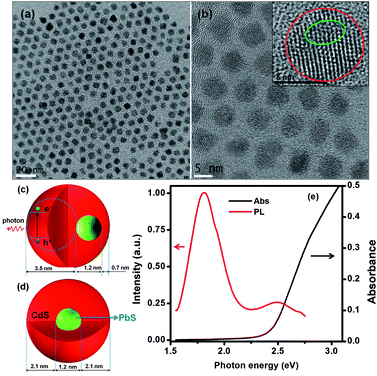
High quality PbS@CdS core@shell QDs have been exclusively prepared via a cation exchange approach.10,19 Because of the mild cation exchange process, the overall diameter of QDs does not change during the reaction.10,19 The shell growth proceeds through the gradual replacement of Pb cations by newly introduced Cd cations in solution, leaving the sulfur lattice almost unchanged,26 resulting in the decrease of PbS core size and the increase of CdS shell thickness. Due to the decrease of the core size, the absorption and PL peak of core QDs show blue shift during the cation exchange process (Fig. S1†).10,19 With more CdS being deposited, i.e., when the shell becomes thicker, an additional emission peak, attributed to CdS, emerges, as we reported previously.10 Another observation during the cation exchange process for NIR core@shell QD synthesis is that, although the size distribution of the entire QDs remains similar to that of parent PbS QDs regardless of shell thickness, the core becomes more heterogeneous with increasing shell thickness and the shell thickness simultaneously becomes non-uniform. Basically, when the shell thickness is rather thin (≤∼0.7 nm), the PbS@CdS QDs still exhibit good core homogeneity with uniform shell thickness.10 However for double-emission QDs, which have relatively thick shells, the cores could be heterogeneous in both size and shape due to the anisotropic nature of the cation exchange approach.10,20Fig. 1a shows the TEM image of specific double-emission QDs to be investigated herein. These core@shell QDs had an average diameter of 5.4 nm, i.e. the same as that of parent PbS QDs, and a similar narrow size distribution. But under high-resolution TEM (Fig. 1b), some cores appeared to have irregular shapes and were off centered, leading to non-uniform shell thicknesses. The schematic demonstration of a case of highly non-concentric core@shell structure is shown in Fig. 1c. Since the growth of the shell up to ∼0.7 nm is generally uniform, the thinnest shell thickness was set at 0.7 nm in this model. Despite certain structural heterogeneity, it is still interesting to statistically estimate the average PbS core size and shell thickness by assuming an ideal core@shell structure model (Fig. 1d). In this model, core@shell QDs are concentric and have a uniform shell thickness. Based on the overall diameter of core@shell QDs estimated from TEM and Pb-to-Cd ratio determined by ICP-OES, the core size was estimated to be ∼1.2 nm and the shell thickness to be ∼2.1 nm (using the method described in our previous work10). Our observation of PbS core emission at 1.80 eV (Fig. 1e, to be discussed below) with the estimated core size of ∼1.2 nm seems consistent in the trend with that reported very recently for ultra-small PbS QDs (diameter: 1 nm with an emission peak of ∼1.64 eV) capped by ligands similar to those used in this work.27 Even though the estimated dimensions may not be very accurate, they help understanding the complicated charge transfer behavior to be discussed in later sections.
Fig. 1e shows the PL and absorption spectra of the double-emission PbS@CdS QDs. Two emission peaks located at 1.80 eV and 2.50 eV originated from the PbS core and CdS shell, respectively, as previously reported.10 With further increase of cation exchange time, the higher-energy emission peak showed a red shift (Fig. S1a†), consistent with increasing CdS dimension.10 It is in clear contrast to the continuous blue shift of the PbS emission peak (the lower-energy peak) with increasing reaction time (Fig. S1a†). Lifetime measurements further confirmed the origin of these two emissions. The decay curve of the PL peak centered at ∼1.80 eV fitted well into a two-component model, yielding the lifetimes of ∼976 ns and 139 ns (Fig. 2a), in agreement with previously reported data for PbS QDs.10,28–30 In the case of 2.50 eV emission, the decay was again bi-exponential (Fig. 2b), yielding two lifetime components of 3 ns and 10 ns that are within the range of those reported for CdS QDs.31–33 As the emission energy of the ultrasmall, nanosized CdS domain studied herein was nearly equal to the reported band gap energy of the bulk CdS material, this 2.50 eV emission peak should not be attributed to the band edge emission of quantum confined CdS. Instead, it is believed to originate from trap states, which typically lead to the longer-wavelength emission as compared to the band edge emission of quantum confined CdS.31,33 The trap-state emission is indeed common in CdS QDs.31,33 Clearly, unlike uniform thin-shell core@shell QDs, where the shell is mainly used to enhance the core emission, the shell showed its own “optical identity” in relatively thicker-shell core@shell QDs. Similar double emissions from the core and shell have also been reported for specifically designed visible-emitting core/shell nanostructures,14,34–36 although overwhelmingly in almost all other papers only core emission was observed.6,7,12,15,19,37–39 By sandwiching a ZnS layer in between CdSe cores and CdSe shells, Peng et al., have found that the CdSe/ZnS/CdSe core/shell/shell QDs can show double color emissions from the CdSe core and shell, respectively.34 The presence of the ZnS layer can largely prohibit the electronic coupling between the CdSe core and the CdSe shell, enabling their emissions.34,35 A similar phenomenon has been found in the chunky rod-shaped Te-doped CdSe/CdS/CdZnSe core/shell/shell nanostructures.36 In our system, however, there is no such a barrier layer intentionally formed in between the emitting core and shell. Another interesting double-emission system was reported by Choi, et al. They have attributed the double emission behavior observed from CdSe/CdS core/shell tetrapods to spatially direct transition and spatially indirect emission across the CdSe/CdS heterojunction,40 with the latter being similar to the emission nature of type II QDs.40,41 Because the indirect transition is expected to lead to a longer lifetime that was not observed in our system, we believe that this mechanism does not play an important role herein.40,41
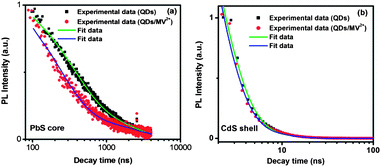 | ||
| Fig. 2 Typical PL decay curves for PbS@CdS QDs measured at the emission peak of (a) 1.80 eV and (b) 2.50 eV in toluene before and after the addition of MV2+, shown on a logarithmic scale. | ||
The evolution of the absorption spectra of PbS/CdS QDs during the cation exchange process is shown in Fig. S1b.† With longer reaction time, thicker-shell QDs were formed that showed enhanced absorption at energy higher than ∼2.5 eV (Fig. S1b,† cyan and magenta lines). The CdS in the thicker-shell QDs showed strong absorption as evidenced by a shoulder at ∼2.75 eV. As the emission spectrum of CdS overlaps with the absorption of the PbS core (Fig. S1a and b†), the energy transfer from the core to the shell is possible. However, certain electrons and holes in higher energy excitons generated in the shell region, which were located relatively far from the core (Fig. 1c, highly non-concentric sphere model), may still get the chance to rapidly and radiatively re-combine, escaping from the emission quenching process induced by the presence of the core in the so-called Dexter energy transfer process occurring at sub-nanometer donor (herein the CdS shell) and acceptor (herein the PbS core) distance. Therefore, the QD emission could be mainly contributed by the shell in the small fraction of core@shell QDs with the core largely deviating from the center. On the other hand, as the efficiency of Förster energy transfer strongly depends on the relative orientation of excitons in the donor (CdS) and acceptor (PbS), statistically mis-oriented excitons in the CdS shell, which did not meet energy transfer conditions, might also be responsible for the shell emission. Both explanations are consistent with the very low emission intensity of CdS in our case. We further examined the ratio of the integrated PL intensity of core-to-shell emissions for thick-shell PbS@CdS QDs synthesized at different reaction times (20 hours versus 60 hours). With increasing reaction time, in addition to the red-shift of the PL peak, it was found that the ratio of the integrated PL intensity from the core to that of the shell decreased from 3.1 to 1.4, highly likely due to the decreased spectral overlap between the emission of the CdS shell and the absorption of the PbS core, although it is difficult to quantitatively separate the absorption of PbS from that of CdS (Fig. S1b†).
Furthermore, we measured the temperature dependence of the PL of double-emission QDs. The PbS@CdS QDs were mixed with a polystyrene solution and drop-dried to fabricate a thin film on a glass substrate. The evolution of the PL spectra of QDs excited at 2.75 eV was recorded at different temperatures from 100 to 323 K. The PL spectra of the QD film at different temperatures could be fitted with two Gaussian peaks corresponding to two different emission bands (Fig. S2†). With decreasing temperature, T, the integrated PL intensity steadily increased for both emission bands in the investigated temperature range of 100–323 K (Fig. 3b) due to the decrease of exciton–phonon interactions.42,43 The intensity of the lower-energy emission band centered at 1.80 eV increased by ∼5 fold, consistent with that reported for well-passivated pure PbS nanocrystals.42 On the other hand, the intensity of the higher-energy emission band only differed by ∼1.7 fold with temperature, which is in good agreement with the reported trap-state emission for pure CdS QDs.44 These results indirectly confirmed the origin (PbS core and CdS shell) of the two emission bands. Moreover, the PL peak positions did not show any significant shift in the investigated temperature range, even at the elevated temperature of 323 K, indicating that the optical properties of these core@shell QDs are thermally stable, which is relevant for outdoor solar cell applications.
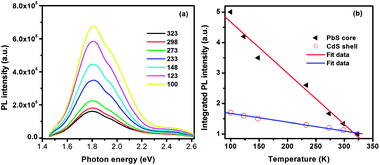 | ||
| Fig. 3 (a) PL spectra of double-emission PbS@CdS QDs as a function of temperature and (b) plot of integrated intensity of PL from the PbS core and CdS shell versus temperature. | ||
3.2 Charge transfer behavior of double-emission QDs
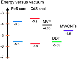
Charge transfer from photoexcited QDs to charge carrier acceptors depends on several factors, such as band alignment, geometric factor and time scale.28,45 As for core@shell QDs, one more factor, i.e., the relative energy alignment of the core and shell, needs to be considered. For a typical type-I alignment, usually only core excitons are taken into consideration. Since both electrons and holes are confined in the core region, they need to overcome the potential offset or tunnel through the shell in order to make the charge transfer process viable. For a type-II alignment, only carriers confined in the core region suffer from the barrier effect from the shell; the charge transfer of these carriers can be largely affected by the presence of the shell. For quasi-type-II QDs, depending on the confinement regime of carriers, they may behave quite similarly to or differently from shell-free QDs.In this work, in order to study the charge transfer behavior of PbS@CdS QDs with double emission, we added MV2+, a well-known electron scavenger, or DDT, a hole scavenger, to PbS@CdS QD solution and analyzed their effect on the PL spectra and lifetime of the two emission bands of the QDs. The redox energy level of MV2+ is around −4.06 eV versus the vacuum level,15,46 and that of DDT is −5.65 eV,47,48 as shown in Fig. 4. As MV2+ shows an absorption peak at an energy higher than 3.1 eV, it does not overlap with any PL band of the QDs, which excludes the Förster energy transfer from the QDs to MV2+.15 Similarly, the DDT absorption does not show any spectral overlap with the QD emission. As a result, emission quenching with the introduction of MV2+ or DDT should be solely correlated with the photo-excited charge transfer process.
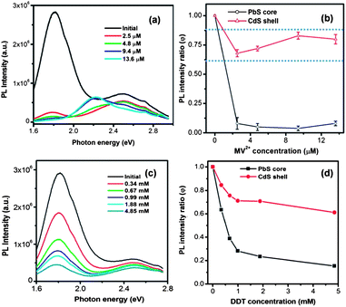
MV2+ was first dissolved in IPA and the MV2+–IPA mixture was added into the QD solution drop by drop until the desired concentration was achieved. As a reference, we added the same amount of pure IPA to the QD sample, which did not cause any significant drop of PL. The PL spectra after MV2+ addition are shown in Fig. 5a. To study the PL quenching behavior quantitatively, we define the PL intensity ratio as
| φ = I/I0 | (1) |
Aiming to identify the driving force of electron injection from the core@shell QDs, we first calculated the conduction and valence band energy levels of the PbS core and CdS shell based on their optical band gaps. Due to the lack of a distinctive excitonic absorption band related to the core heterogeneity, the band-edge emission peak was used to calculate the bandgap of the PbS core. By assuming the symmetric shift of energy levels with respect to those in bulk PbS,49–51 the HOMO and LUMO levels of the PbS core were estimated to be −5.6 eV and −3.8 eV, respectively. The HOMO and LUMO levels of the CdS shell were estimated to be −5.9 eV and −3.2 eV, respectively, based on the absorption data, instead of the emission data as the CdS emission is attributed to trap-state emission herein.25 Since the LUMO levels of both PbS core (−3.8 eV) and CdS shell (−3.2 eV) were higher than the redox energy level of MV2+ (−4.06 eV), electron transfer from both PbS and CdS to MV2+ was plausible. Nonetheless, the LUMO level of the former was 0.6 eV lower, suggesting a smaller driving force for the MV2+ reduction by the PbS core than by the CdS shell. Further considering the geometric factor, as the PbS core was covered by CdS, the photoexcited electrons in the shell should be closer to MV2+ as compared to those in the PbS core and hence be more easily transferred.45 Therefore, from both energetic and geometric points of view, it would be expected that the excitons in the CdS shell were quenched at a higher efficiency, but we indeed observed the opposite.
In order to understand this interesting observation, we further compared the fluorescence decay behavior of the QDs before and after the introduction of MV2+ and analyzed charge-transfer rate constants derived from the fluorescence lifetime. As was the case when MV2+ was absent, the decay of the PbS core emission in the presence of MV2+ could be fitted by two exponential decay terms, which varied with the concentration of MV2+. To estimate the charge transfer rate constant, the average PL lifetime was calculated. It was found that with the presence of 2.5 μM of MV2+, the average PL lifetime of the core largely decreased from around 900 ns to 790 ns, as shown in Fig. 2a. As we mentioned above, the PL quenching of the QDs in our case is likely due to the charge transfer rather than energy transfer. Thus, the observed decrease of lifetime must be a result of the photoexcited electron transfer from the PbS core to MV2+. The charge-transfer rate constant (ket) was then estimated using the following equation:52
| ket = 1/τ(PbS core/MV2+) − 1/τ(PbS core) | (2) |
Fig. S3† shows the variation of ket with MV2+ concentration. It is clearly seen that with the increase of MV2+ concentration, the charge-transfer rate significantly increased to reach a value as high as 1.6 × 10⁶ s−1, comparable with that reported for the PbS/TiO2 system by Hyun et al.28 In a big contrast, as shown in Fig. 2b and S4a,† the PL lifetimes of the CdS shell (PL peak at 2.50 eV) before and after the addition of MV2+ did not show any significant difference, suggesting that the charge transfer occurs at a much slower rate with respect to the rapid radiative recombination (several ns) in the CdS shell. The fact that charge transfer cannot strongly compete with the emission process in terms of time scale is likely responsible for less efficient quenching observed in the CdS shell. These results demonstrate that the thermodynamic factor is not the only important factor; for the specific double-emission QDs studied herein, the time scale factor appears to be dominant for the PL quenching and charge transfer behavior for excitons in the shell.
In addition to the electron transfer, we also examined the photoexcited hole transfer behavior of the PbS@CdS QDs with double emission. After adding DDT into the QD dispersion, the PL intensity of both the PbS core and the CdS shell decreased with increasing DDT concentration (Fig. 5c and d). It is known that hole transfer from a semiconductor nanocrystal to a thiol is energetically favorable if the thiol redox energy level is situated at a higher energy level than the HOMO of the nanocrystal.47 In our case, the HOMO level of the core was similar to that of DDT. As for the CdS shell, its HOMO level was lower. But it should be noted that the estimation of the CdS HOMO level was only approximate. Similar to what we observed with the electron scavenger MV2+, the PL quenching of the PbS core was more obvious than that of the CdS shell (Fig. 5d) due to the more efficient hole transfer process from the PbS core to DDT as compared to from the CdS shell. Again this less efficient hole transfer was correlated with unfavorable time competition between charge transfer and radiative recombination in the shell (Fig. S4b and S5†).
3.3 Theoretical calculation of electron and hole wave functions
Further insights into the charge transfer behavior in the double-emission core@shell QDs with relatively thick shell were obtained by conducting electron and hole wave function calculations. As mentioned above, the core was not homogenous and the actual sample could be a mixture of ideal QDs with a uniform shell thickness (Fig. 1d), QDs in the extreme configuration (Fig. 1c) and QDs in an intermediate configuration between the two extreme cases. Based on TEM observation, these intermediate QDs represented the largest portion. However in order to avoid excessive complexity, we calculated the wave function of a PbS@CdS QD for the concentric model (Fig. 1d), assuming the core radius and shell thickness to be 0.6 and 2.1 nm, respectively.28 Bulk PbS and CdS were used to evaluate the band structure and the electron and hole effective masses.25Fig. 6 shows the radial distribution functions of the 1s electron and hole in a PbS@CdS QD. Both the electron and hole wave functions spread into the CdS layer, with the electron delocalizing over the entire QD, and the hole leaking into the shell with a limited distance of ∼1.4 nm. Fig. 6 indicates that this ideal PbS@CdS QD has indeed the quasi-type II structure, although, based on the energy levels, it should be of type I (Fig. 4). Then, straightforwardly, it could be predicted that electron transfer is feasible, while hole transfer is not. However as we mentioned above, many double-emission QDs indeed showed a non-concentric spherical structure (Fig. 1c), which meant that the shell thickness was not uniform and some parts were much thinner than the other parts. In this case, the photo-generated hole in the core could still have the chance to leak to the surface through the thin-shell part and interact with DDT. Taking the highly non-concentric structural model as an example (Fig. 1c), assuming that the non-uniform cation exchange process starts at the shell thickness of 0.7 nm and the overall QD size is 5.4 nm, then the thinnest shell is 0.7 nm and the thickest shell is 3.5 nm in thickness. In this case, based on the above calculation, both the electron and hole of the core can tunnel through the thinnest part. The quenching of the core emission in the presence of DDT thus confirmed the leakage and availability of the holes on the surface as well as the presence of certain amounts of non-uniform-shell QDs in this sample.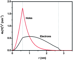 | ||
| Fig. 6 Normalized radial distribution functions for 1s electron and hole levels of a PbS@CdS core@shell QD with the core size of 0.6 nm radius and shell thickness of 2.1 nm. | ||
3.4 Core size effect
The specific double-emission core@shell QDs described above had a very small core size (∼1.2 nm) and relatively large shell thickness of ∼2.1 nm. It is also interesting to investigate the charge transfer behavior of PbS@CdS core@shell QDs with varying core sizes and shell thicknesses. Since when the shell thickness is 0.7 nm, in theory there is no problem for the electron generated in the core to reach the surface (Fig. S6†), we synthesized and studied PbS@CdS QDs with a constant shell thickness of 0.7 nm and different core sizes ranging from 3.2 to 5.8 nm.10 As reported in our previous work, the PbS@CdS QDs with shell thickness equal to or less than 0.7 nm show a narrow core size distribution and quite uniform shell thickness.10 In addition, they only show a single strong emission peak from the core (Fig. S7†). As shown in Fig. 7, adding IPA did not cause any drop of PL of the core QDs, while their response to the addition of MV2+–IPA varied with the core size. The core PL was nearly completely quenched (φ ∼ 0) when the core diameter was ≤4.4 nm, while barely affected when it was ≥5 nm (φ ∼ 1). Such a difference should be mainly dictated by the relative energy level alignment between the PbS cores and MV2+; smaller the QD size is, higher the LUMO level is, and hence larger driving force for the charge transfer from the core to MV2+. This finding was further confirmed by the theoretical calculation of the electron energy of core/shell QDs as a function of PbS diameter. The uniform core size and shell thickness allowed us to perform good calculations. As shown in Fig. S8,† for the QDs with core diameter <4.25 nm, the electron energy is >−4.06 eV (MV2+ potential), suggesting that the electron excited in PbS can “fall” into the MV2+ potential and cause PL quenching. For the QDs with core diameter >4.25 nm, the electron cannot be efficiently transferred to the MV2+ in principle. The critical diameter of 4.25 nm is very close to the experimentally observed transition range of 4.4–5 nm. Although it is also possible that from 4.4 to 5 nm, the decrease of the number of MV2+ molecules per unit area of the QD surface causes less efficient quenching due to the increase of the surface area by 30%; this 30% increase cannot absolutely explain the dramatic variation in quenching (from 100% to 0%). The thermodynamic factor is playing an important role in these uniform 0.7 nm thin shell core@shell QDs.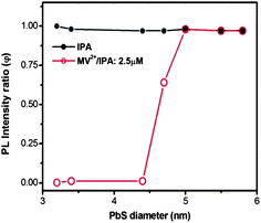 | ||
| Fig. 7 PL intensity ratio (φ) with the addition of IPA or MV2+ (2.5 μM)/IPA as a function of PbS diameter in PbS@CdS QDs. The CdS shell thickness is ∼0.7 nm. The concentration of QDs is 2.5 μM. | ||
3.5 Shell thickness effect
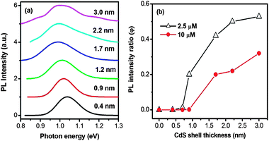
We further studied how the shell thickness affects the charge transfer of the core@shell QDs. To this end, we synthesized PbS@CdS QDs of different shell thicknesses and same core size. Since the core size changes during the shell formation process, the PbS@CdS QDs of a similar core size, yet different shell thicknesses, have to be synthesized by choosing differently sized parent PbS QDs together with different reaction parameters, such as reaction temperature and time.10 As shown in Fig. 8a, the emission peak position for all the samples was around 1.0–1.05 eV, corresponding to a similar PbS core size of ∼3.6 nm.10 The average CdS shell thickness was varied from 0.4 to 3.0 nm, estimated by deducting the core size from the overall QD size from TEM observations. The core PL spectra of PbS@CdS QDs without MV2+ are shown in Fig. 8a. The PL of core QDs dropped after being mixed with a very low concentration (2.5 μM) of MV2+. As shown in Fig. 8b, when the shell thickness was ≤0.7 nm, the PL is nearly completely quenched (i.e., φ ∼ 0). When the shell got thicker, the quenching became less efficient. At the estimated average shell thickness of 3.0 nm, the core QDs maintained about 55% of the initial PL (φ ∼ 0.55). So the quenching changed from 100% to 45%. Again the size increase of the QDs cannot solely explain this variation. Such a thickness effect on the quenching behavior must reflect the dependence of the charge transfer efficiency on the probability of electrons leaking to the surface in thicker shell QDs. When the concentration of MV2+ was further increased to 10 μM, the trend was similar. The value of φ increased with increasing shell thickness, but in all cases, its values were smaller than those observed with 2.5 μM of MV2+ (Fig. 8b). The concentration-dependent quenching behavior implies that the charge transfer process is also affected by the availability of MV2+ when the electron tunnels to the surface in the case of relatively thick shell QDs. Considering the quite low concentration (2.5 μM) of MV2+, yet its significant quenching effect, it is clear that when the shell is thin (e.g., ≤0.7 nm), the charge transfer is apparently overwhelming as compared to the radiative recombination process. Nonetheless, when the shell gets thicker, the probability of a limited number of electrons leaking to the QD surface and their probability of reacting with MV2+ in close proximity start to play a role in the competition between charge transfer and radiative recombination. In the latter case, the CdS shell clearly serves as an efficient electron transfer barrier. This finding provides insights into designing and optimizing NIR core@shell QD-based solar cells.3.6 Charge transfer from QDs to MWCNTs
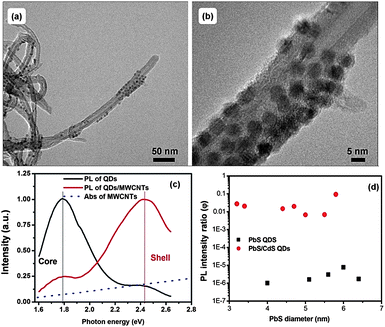
To realize high performance solar cells, QDs are required to show highly efficient charge transfer and good stability.23 Compared to the shell-free PbS QDs, the core@shell structured PbS@CdS QDs exhibit significantly higher QY, as high as 67% for the optimal CdS shell thickness of 0.7 nm, and better photo- and thermal stability.10 In addition, as we mentioned above, even though in theory the larger band-gap CdS shell serves as a charge transfer barrier, photoexcited electrons can still be efficiently transferred to small MV2+ molecules, especially when the shell is thin. Therefore, it is interesting to explore the use of high optical quality core@shell QDs in the application of solar cells. Recently our group observed that MWCNTs can improve the electron transfer and transport in the PV device fabricated with PbS QD-decorated MWCNTs and poly(3-hexylthiophene).23 It is worthwhile to further investigate the electron transfer behavior of the core@shell QDs after their combination with MWCNTs in solution. The PbS@CdS QDs were well attached to MWCNTs, forming the PbS@CdS QD/MWCNT nano-architectured material, as can be clearly seen from both the low magnification and high-resolution TEM images (Fig. 9a and b). For comparison, we also fabricated PbS QD-anchored MWCNTs as we reported previously.23 We then studied the PL intensity and lifetime variation of the QDs after their coupling with MWCNTs.As shown in Fig. 9c, the bimodal PL pattern of the double-emission PbS@CdS QDs was reversed after the hybridization, with significant quenching of the core emission similar to the QD/MV2+ case. In addition, the average lifetime of the PbS core also largely decreased after their combination with the MWCNTs. Either energy transfer53,54 or charge transfer23 to MWCNTs can lead to the decrease of PL of the QDs, depending on the distance between the QDs and MWCNTs and their optical characteristics. Normally, charge transfer may dominate in a short distance of a few nanometers, while at slightly longer distance the energy transfer is dominant.53,54 As the MWCNTs absorb less in the optical spectral range of the core emission than the shell emission (Fig. 9c), we do not think that the quenching is mainly dominated by the energy transfer process, neither the reverse of the PL pattern (i.e., the reverse of the intensity difference between two PL peaks). Further considering the intimate contact between the QDs and the MWCNTs and their relative band alignment (Fig. 4), we can reasonably conclude that the decrease of PL is mainly attributed to electron transfer, instead of energy transfer, from the photoexcited PbS cores to MWCNTs, although we cannot absolutely rule out the energy transfer between the core@shell QDs and the MWCNTs. The faster quenching of the core emission is again correlated with favorable time competition of the charge transfer process, with a rate constant of 2 × 10⁷ s−1 calculated from PL lifetime variation (734 ns for QDs versus 41 ns for QD/MWCNTs), versus radiative recombination in the core as compared to that in the shell. For the CdS shell, in contrast, there was no significant change in its PL lifetime with the hybridization of the MWCNTs. Similar significant quenching due to electron transfer has also been observed in the PbS-QD/MWCNT system, as confirmed by significantly enhanced photocurrent generation in the NIR regime.23 Moreover, the charge transfer has also been reported in the similarly coupled hybrid system of CdS QDs and CNTs.55 As the QDs on the surface of the MWCNTs seem close, it may be questioned whether there is energy transfer between the QDs, which can also cause PL quenching.28 To testify this, we have performed three sets of PL measurements on QDs in solution, in films and after hybridization with CNTs in films. Two types of samples were examined: thin-shell and thick-shell core/shell QDs (Fig. S9†). In general, the energy transfer between QDs could lead to the red shift of PL peaks in addition to PL quenching. After casting QDs from solution into films, they became closer, possibly enabling the energy transfer. As shown in Fig. S9,† the red shift of the PbS emission peak of the thin-shell QDs was quite obvious, while negligible for thick-shell QDs, suggesting the presence of the energy transfer among thin-shell QDs. Once hybridized with CNTs, both types of QDs showed no peak shift with respect to the corresponding QDs in solution, indicating that although the QDs are close on the surface of the CNTs, the energy transfer is negligible. The sharp drop of the PL intensity of the thin-shell QDs and the dramatic change of the ratio of core-to-shell emission of thick-shell QDs (i.e., double emission QDs) must be mainly attributed to the QD–CNT interactions.
Furthermore we studied the size effect on the charge transfer behavior in the PbS-QD/MWCNTs and PbS@CdS-QD/MWCNTs with a constant CdS shell thickness of 0.7 nm (so these PbS@CdS QDs showed single emission bands) in the suitable core size range of 3.2–5.8 nm. Although the quenching for the shell-free PbS QDs was several orders of magnitude higher, most emission of the PbS@CdS QDs was also efficiently quenched by MWCNTs with φ reaching values as low as 1%. These results suggest that the excitons generated in the PbS@CdS QDs upon illumination can be efficiently separated via electron transfer to the MWCNTs, even though in theory the CdS shell serves as a barrier. Further taking their higher optical and thermal stability into consideration, these new core@shell QDs are very promising for solar cell applications.
4. Conclusions
In conclusion, this work investigated the charge transfer behavior of double- and single-emission PbS@CdS core@shell QDs in the presence of charge carrier acceptors. The double-emission of the PbS@CdS QDs with a core size of 1.2 nm and a shell thickens of 2.1 nm was explained by proposing a highly non-concentric structure model. The charge transfer behavior was discussed in terms of energy levels and spatial alignment of conduction- and valence-band edges, as well as time scales. The less efficient PL quenching and thereby less efficient charge transfer from the CdS shell as compared to the PbS core are attributed to unfavorable time competition of the charge transfer process relative to the fast radiative recombination process in the shell. The effect of the core size and shell thickness of single-emission core@shell QDs on charge transfer was also examined. It was found that when the shell is as thin as 0.7 nm, the energy level alignment of the QD with respect to charge carrier scavengers favors PL quenching and charge transfer from the core when the core size is smaller than 4.5 nm. With a thicker shell, the probability of a limited number of electrons leaking to the QD surface and reacting with MV2+ in close proximity starts to play a role in the competition between charge transfer and radiative recombination. The hybridization of the 0.7 nm thick-shell PbS@CdS QDs with MWCNTs again gives rise to very efficient electron transfer from the photoexcited PbS core to MWCNTs in the investigated core size range of ∼3–6 nm. Along with significantly improved stability of these core@shell QDs as compared to pure PbS QDs, these findings suggest that the PbS@CdS core@shell QDs are very promising for the potential development of highly efficient and more stable PV devices.Author contributions
The manuscript was written through contributions of all authors. All authors have given approval to the final version of the manuscript.Additional information
The authors declare no competing financial interest.Acknowledgements
Thanks to Dr A. Vomiero for the discussion of this work. Financial support from the Natural Sciences and Engineering Research Council of Canada, Canadian Solar Inc. and OLA Display Corp. in the context of a NSERC-Strategic grant is greatly appreciated. The authors also acknowledge the financial support from the Fonds Québécois de Recherche sur la Nature et les Technologies. Dr H. Y. Liang acknowledges FRQNT for a graduate scholarship.Notes and references
- A. P. Alivisatos, Science, 1996, 271, 933–937 CAS.
- A. L. Rogach, A. Eychmüller, S. G. Hickey and S. V. Kershaw, Small, 2007, 3, 536–557 CrossRef CAS PubMed.
- X. Michalet, F. F. Pinaud, L. A. Bentolila, J. M. Tsay, S. Doose, J. J. Li, G. Sundaresan, A. M. Wu, S. S. Gambhir and S. Weiss, Science, 2005, 307, 538–544 CrossRef CAS PubMed.
- R. Weissleder, Nat. Biotechnol., 2001, 19, 316–317 CrossRef CAS PubMed.
- M. Danek, K. F. Jensen, C. B. Murray and M. G. Bawendi, Chem. Mater., 1996, 8, 173–180 CrossRef CAS.
- B. O. Dabbousi, J. Rodriguez-Viejo, F. V. Mikulec, J. R. Heine, H. Mattoussi, R. Ober, K. F. Jensen and M. G. Bawendi, J. Phys. Chem. B, 1997, 101, 9463–9475 CrossRef CAS.
- S. A. Ivanov, A. Piryatinski, J. Nanda, S. Tretiak, K. Zavadil, W. O. Walalce, D. Werder and V. I. Klimov, J. Am. Chem. Soc., 2007, 129, 11708–11719 CrossRef CAS PubMed.
- A. C. Bartnik, F. W. Wise, A. Kigel and E. Lifshitz, Phys. Rev. B: Condens. Matter Mater. Phys., 2007, 75, 245–424 CrossRef.
- H. G. Zhao, D. F. Wang, T. Zhang, M. Chaker and D. Ma, Chem. Commun., 2010, 46, 5301–5303 RSC.
- H. G. Zhao, N. Wu, M. Chaker and D. Ma, J. Mater. Chem., 2011, 21, 8898–8904 RSC.
- S. Kim, B. Fisher, H. J. Eisler and M. Bawendi, J. Am. Chem. Soc., 2003, 125, 11466–11467 CrossRef CAS PubMed.
- B. De Geyter, Y. Justo, I. Moreels, K. Lambert, P. F. Smet, D. Van Thourhout, A. J. Houtepen, D. Grodzinska, C. de Mello Donega, A. Meijerink, D. Vanmaekelbergh and Z. Hens, ACS Nano, 2010, 5, 58–66 CrossRef PubMed.
- R. Debnath, O. Bakr and E. H. Sargent, Energy Environ. Sci., 2011, 4, 4870–4881 CAS.
- F. Li, D. I. Son, T. W. Kim, E. Ryu, S. W. Kim, S. K. Lee and Y. H. Cho, Appl. Phys. Lett., 2009, 95, 061911 CrossRef.
- L. Dworak, V. V. Matylitsky, V. V. Breus, M. Braun, T. Basche and J. Wachtveitl, J. Phys. Chem. C, 2011, 115, 3949–3955 CAS.
- Z. J. Ning, H. N. Tian, C. Z. Yuan, Y. Fu, H. Y. Qin, L. C. Sun and H. Ågren, Chem. Commun., 2011, 47, 1536–1538 RSC.
- S. Itzhakov, H. Shen, S. Buhbut, H. Lin and D. Oron, J. Phys. Chem. C DOI:10.1021/jp312190x.
- E. Ryu, S. Kim, E. Jang, S. Jun, H. Jang, B. Kim and S.-W. Kim, Chem. Mater., 2009, 21, 573–575 CrossRef CAS.
- J. Pietryga, D. Werder, D. Williams, J. Casson, R. Schaller, V. Klimov and J. Hollingworth, J. Am. Chem. Soc., 2008, 130, 4879–4885 CrossRef CAS PubMed.
- K. Lambert, B. De Geyter, I. Moreels and Z. Hens, Chem. Mater., 2009, 21, 778–780 CrossRef CAS.
- L. Cademartiri, J. Bertolotti, R. Sapienza, D. S. Wiersma, V. Kitaev and G. A. Ozin, J. Phys. Chem. B, 2006, 110, 671–673 CrossRef CAS PubMed.
- H. G. Zhao, M. Chaker and D. Ma, J. Phys. Chem. C, 2009, 113, 6497–6504 CAS.
- D. F. Wang, J. K. Baral, H. G. Zhao, B. A. Gonfa, V. Truong, M. A. E. Khakani, R. Izquierdo and D. Ma, Adv. Funct. Mater., 2011, 21, 4010–4018 CrossRef CAS.
- L. Cademartiri, E. Montanari, G. Calestani, A. Migliori, A. Guagliardi and G. A. Ozin, J. Am. Chem. Soc., 2006, 128, 10337–10346 CrossRef CAS PubMed.
- J. W. Haus, H. S. Zhou, I. Honma and H. Komiyama, Phys. Rev. B: Solid State, 1993, 47, 1359–1365 CrossRef CAS.
- D. H. Son, S. M. Hughes, Y. Yin and A. P. Alivisatos, Science, 2004, 306, 1009–1012 CrossRef CAS PubMed.
- J. H. Warner, E. Thomsen, A. R. Watt, N. R. Heckenberg and H. Rubinsztein-Dunlop, Nanotechnology, 2010, 16, 175–179 CrossRef PubMed.
- B. R. Hyun, Y. W. Zhong, A. C. Bartnik, L. Sun, H. D. Abruña, F. W. Wise, J. D. Goodreau, J. R. Matthews, T. M. Leslie and N. F. Borrelli, ACS Nano, 2008, 2, 2206–2212 CrossRef CAS PubMed.
- J. Warner, E. Thomsen, A. R. Watt, N. R. Heckenberg and H. Rubinsztein-Dunlop, Nanotechnology, 2005, 16, 175–179 CrossRef CAS PubMed.
- D. F. Wang, H. G. Zhao, N. Wu, M. A. E. Khakani and D. Ma, J. Phys. Chem. Lett., 2010, 1, 1030–1035 CrossRef CAS.
- H. L. Chou, C. H. Tseng, K. C. Pillai, B. J. Hwang and L. Y. Chen, J. Phys. Chem. C, 2011, 115, 20856–20863 CAS.
- J. R. Lakowicz, I. Gryczynski, Z. Gryczynski and C. J. Murphy, J. Phys. Chem. B, 1999, 103, 7613–7620 CrossRef CAS.
- J. Ouyang, J. A. Ripmeester, X. Wu, D. Kingston, K. Yu, A. Joly and W. Chen, J. Phys. Chem. C, 2007, 111, 16261–16266 CAS.
- D. Battaglia, B. Blackman and X. Peng, J. Am. Chem. Soc., 2005, 127, 10889–10897 CrossRef CAS PubMed.
- E. A. Dias, A. F. Grimes, D. S. English and P. Kambhampati, J. Phys. Chem. C, 2008, 112, 14229–14232 CAS.
- Z. Deutsch, O. Schwartz, R. Tenne, R. Popovitz-Biro and D. Oron, Nano Lett., 2012, 12, 2948–2952 CrossRef CAS PubMed.
- D. Oron, M. Kazes and U. Banin, Phys. Rev. B: Condens. Matter Mater. Phys., 2007, 75, 035330 CrossRef.
- M. Jones, S. Kumar, S. S. Lo and G. D. Scholes, J. Phys. Chem. C, 2008, 112, 5423–5431 CAS.
- Y. Chen, J. Vela, H. Htoon, J. L. Casson, D. J. Werder, D. A. Bussian, V. I. Klimov and J. A. Hollingsworth, J. Am. Chem. Soc., 2008, 130, 5026–5027 CrossRef CAS PubMed.
- C. L. Choi, H. Li, A. C. K. Olson, P. K. Jain, S. Sivasankar and A. P. Alivisatos, Nano Lett., 2011, 11, 2358–2362 CrossRef CAS PubMed.
- S. S. Lo, T. Mirkovic, C.-H. Chuang, C. Burda and G. D. Scholes, Adv. Mater., 2010, 23, 180–197 CrossRef PubMed.
- L. Turyanska, A. Patane, M. Henini, B. Hennequin and N. R. Thomas, Appl. Phys. Lett., 2007, 90, 101913 CrossRef.
- G. I. Maikov, R. Vaxenburg, A. Sashchiuk and E. Lifshitz, ACS Nano, 2010, 4, 6547–6556 CrossRef CAS PubMed.
- D. Kim, T. Mishima, K. Tomihira and M. Nakayama, J. Phys. Chem. C, 2008, 112, 10668–10673 CAS.
- B.-R. Hyun, A. C. Bartnik, L. Sun, T. Hanrath and F. W. Wise, Nano Lett., 2011, 11, 2126–2132 CrossRef CAS PubMed.
- M. Grätzel, Nature, 2001, 414, 338–344 CrossRef PubMed.
- S. F. Wuister, C. D. Donega and A. Meijerink, J. Phys. Chem. B, 2004, 108, 17393–17397 CrossRef CAS.
- J. Jasieniak, M. Califano and S. E. Watkins, ACS Nano, 2011, 5, 5888–5902 CrossRef CAS PubMed.
- S. A. McDonald, G. Konstantatos, S. Zhang, P. W. Cyr, E. J. D. Klem, L. Levina and E. H. Sargent, Nat. Mater., 2005, 4, 138–142 CrossRef CAS PubMed.
- H. C. Leventis, F. O'Mahony, J. Akhtar, M. Afzaal, P. O'Brien and S. A. Haque, J. Am. Chem. Soc., 2010, 132, 2743–2750 CrossRef CAS PubMed.
- A. Braga, S. Giménez, I. Concina, A. Vomiero and I. Mora-Seró, J. Phys. Chem. Lett., 2011, 2, 454–460 CrossRef CAS.
- K. R. Gopidas, M. Bohorquez and P. V. Kamat, J. Phys. Chem., 1990, 94, 6435–6440 CrossRef CAS.
- E. Shafran, B. D. Mangum and J. M. Gerton, Nano Lett., 2010, 10, 4049–4054 CrossRef CAS PubMed.
- V. Biju, T. Itoh, Y. Baba and M. Ishikawa, J. Phys. Chem. B, 2006, 110, 26068–26074 CrossRef CAS PubMed.
- X. Li, Y. Jia and A. Cao, ACS Nano, 2010, 4, 506–512 CrossRef CAS PubMed.
Footnote |
| † Electronic supplementary information (ESI) available: The PL and absorption spectra of PbS@CdS QDs in solution and in films with and without the combination of MWCNTs, Gaussian curve fit to the PL spectra of representative QD film samples, PL lifetime and charge transfer rate from QDs to electron or hole scavengers, radial distribution functions for 1s electron levels of the PbS@CdS core@shell QD with a different core size and constant shell thickness. See DOI: 10.1039/c3nr03691j |
| This journal is © The Royal Society of Chemistry 2014 |

