Strong localized surface plasmon resonance effects of Ag/TiO2 core–shell nanowire arrays in UV and visible light for photocatalytic activity†
Hyeonjin
Eom
ab,
Joo-Yun
Jung
b,
Yosep
Shin
b,
Sarah
Kim
b,
Jun-Hyuk
Choi
b,
Eungsug
Lee
b,
Jun-Ho
Jeong
*b and
Inkyu
Park
*ac
aDepartment of Mechanical Engineering, Korea Advanced Institute of Science and Technology (KAIST), Daejeon, 305-701, Korea. E-mail: inkyu@kaist.ac.kr; Fax: +82-42-350-3210; Tel: +82-42-350-3240
bDepartment of Nano Manufacturing Technology, Korea Institute of Machinery and Materials (KIMM), Daejeon 305-343, Korea. E-mail: jhjeong@kimm.re.kr; Fax: +82-42-868-7123; Tel: +82-42-868-7604
cKI for the NanoCentury, Korea Advanced Institute of Science and Technology (KAIST), Daejeon, 305-701, Korea
First published on 30th September 2013
Abstract
Periodic arrays of silver/titanium dioxide (Ag/TiO2) open core–shell nanowires have been investigated as enhanced plasmonic photocatalytic structures. Sequential top-down nanofabrication processes based on nanoimprinting, oblique angle evaporation, and selective electrodeposition were employed for the fabrication of various TiO2-shelled Ag nanowire arrays. Numerical simulation proves that the periodic array of Ag/TiO2 core–shell nanowire structures enables strong localized surface plasmon resonance (LSPR), which improves the electron generation and photocatalytic activities of the TiO2 shell. Enhanced photocatalytic performance was confirmed by the decomposition of methylene blue solution. Furthermore, the film composed of a Ag/TiO2 core–shell nanowire array shows photocatalytic reproducibility in the UV and visible light regions and mechanical robustness due to the periodic grating-like metal nanostructures. Our method allows reliable, controllable, and facile fabrication of large-scale plasmonic photocatalytic nanostructured films on various substrates such as glass, polymer, etc.
1 Introduction
Titanium dioxide (TiO2) is a well-known photocatalytic material with major applications such as environmental purification,1 bacterial inactivation2 and carbonic acid gas decomposition.3 Approaches for enhancing the photocatalytic performance of TiO2 could be classified into several categories: improvement of crystallinity and increase of the surface area by using nanostructures;4 extension of light adsorption by doping with non-metallic elements;5 and modulation of electron trap system by doping6,7 or embedding8–10 with metallic elements. In particular, the enhanced photocatalytic activities of metal-embedded TiO2 can be explained by the metal's electron donation11 to TiO2, which assists the formation of superoxide radical anion O2−˙ on the surface.12 Furthermore, noble metal nanoparticles embedded in the TiO2 structures have been shown to enhance the localized surface plasmon resonance (LSPR), which can extend the light absorption to the visible-light region and improve the photocatalytic activity of TiO2.13–15 Therefore, the metal embedded photocatalytic oxides are called as plasmonic photocatalysts.10,16,17 For example, an Ag nanodot arrangement in TiO2 nanostructures18 and Ag nanoparticles embedded between TiO2 and SiO2 thin films17 were studied as plasmonic catalysts based on the enhancement by the LSPR phenomenon. However, most of the aforementioned studies have used randomly distributed metal nanostructures within the TiO2 matrix, which have limited the uniformity and reproducibility of the plasmonic photocatalytic activities of the TiO2 matrix for self-cleaning films and other applications. Furthermore, there have not been sufficient in-depth analysis of the plasmonic photocatalytic effects of metal–TiO2 hybrid structures that cover overall aspects including numerical simulation of the LSPR phenomena, ultraviolet-visible (UV-Vis) spectroscopy measurements, photocatalysis experiments, and their correlations.In the present work, periodic arrays of Ag/TiO2 open core–shell nanowire structures were utilized for plasmonic photocatalytic functions. Periodic arrays of one-dimensional metal nanostructures have been previously used for wire-grid polarizers19 and transparent electrodes.20,21 To the best knowledge of the authors, this is the first work on the utilization of periodic arrays of one dimensional metal nanostructures with thin TiO2 layers film for highly efficient plasmonic photocatalytic functions in ultraviolet (UV) and visible light. The periodicity of the metal nanostructured film provides an enhanced LSPR effect, which can improve the photocatalytic activity of the surface TiO2 layer. The Ag/TiO2 open core–shell nanowire array consists of three layers: a polymer resin template patterned by nanoimprint lithography; an Ag thin film deposited by oblique angle evaporation; and a TiO2 thin film coated by an electrodeposition process. The structure and fabrication process of our Ag/TiO2 open core–shell nanowire array provides unique advantages as follows: firstly, the nanoimprinting lithography enables a facile, high-throughput, and highly reproducible fabrication of periodic nanostructure arrays over a large area. Secondly, selective oxide deposition on the surface of metal nanowire structure by electrochemical deposition allows the fabrication of various uniform core–shell nanostructures.
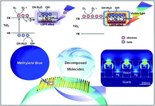
Scheme 1 shows the mechanism of the LSPR-enhanced photocatalytic reaction on the surface of an Ag/TiO2 open core–shell nanowire array in UV and visible light. As shown in the inset, the photon absorption induces a strong LSPR phenomenon at the Ag–TiO2 interface, which enhances the generation of electron–hole pairs.22 Upon exposure to the UV light, electrons in the valence band of TiO2 are excited to the conduction band and Ag prevents the recombination of the electron–hole pairs by capturing the free electrons from TiO2. The holes are then used for the generation of OH˙ radicals. Simultaneously, electrons are used for the generation of O2−˙ radicals.11 Furthermore, the LSPR effect on the surface of Ag provides electrons to TiO2 by diffusion. In visible light, the photon absorption induces a strong LSPR phenomenon at the Ag–TiO2 interface, which enhances the generation of electron–hole pairs. The electrons generated by the LSPR effect diffuse into the TiO2 shells, enhancing the generation of O2−˙ radicals.3,15,23 Also, the holes generated in Ag are used for the generation of OH˙ radicals. Both O2−˙ and OH˙ radicals play a crucial role in the photocatalytic degradation of organic contaminant molecules. Furthermore, spatial charge prevents the direct recombination of electrons and holes, which causes the enhancement of photocatalytic behavior.23 Since the periodicity and geometry of the nanowire array affect the LSPR efficiency, the nanowire array shows improved photocatalytic activity. In this work, we have conducted both numerical and experimental analysis of the LSPR-enhanced photocatalytic activities of Ag/TiO2 open core–shell nanowire arrays with various geometrical configurations. Also, the high photocatalytic efficiency of the Ag/TiO2 open core–shell nanowire array was verified by comparison with Ag/TiO2 dual layer and TiO2 single layer thin films.
2 Experimental
2.1 Fabrication of periodic Ag NW array and TiO2 coating
The templates for the formation of Ag NWs were fabricated by nanoimprint lithography (NIL). UV-curable resin (MonoMat®, Molecular Imprint Inc.) was spray-coated onto a quartz substrate, pressed with a mold with a 100 nm width/200 nm pitch line array pattern and cured by a UV light source. Then, Ag NW array structures with various geometries were fabricated on the nanoscale line array patterns of resin by thermal evaporation of Ag thin film with an oblique angle method.24 Then, a TiO2 layer was electrodeposited on the surface of the Ag NW array which performed as a working electrode. Here, an electrolyte consisting of 0.1 M NH4NO3 and 0.05 M (NH4)2TiF6 in DI water was used. A three electrode cell configuration with an Ag NW array as a working electrode, platinum (Pt) coated titanium (Ti) plate as a counter electrode, and Ag/AgCl (saturated KCl) electrode as a reference electrode was used at a room temperature condition with a stirring rate of 400 rpm. A constant potential of −1.1 V was applied for 100 s by using a potentiostat/galvanostat (601D, CH Instruments, Inc.) for the deposition of a sub-50 nm thick TiO2 thin film (see the ESI† for a detailed procedure). For the formation of anatase-phase TiO2 with better photocatalytic capability than the electrodeposited gel-phase TiO2,25 some samples on the quartz substrate were annealed at 300 °C for 20 min. The Ag/TiO2 core–shell nanowire array was also fabricated on the polyethylene terephthalate (PET) substrate by using the same process as the samples on the quartz substrate. However, due to the low thermal stability of the PET substrate, thermal annealing was not conducted for these samples. Therefore, only a gel-phase Ag/TiO2 core–shell nanowire array was used for experiments in the case of samples on the PET substrate.2.2 Fabrication of Ag/TiO2 dual layer and TiO2 single layer thin films
Ag/TiO2 dual layer and TiO2 single layer films were also fabricated and evaluated for comparison with Ag/TiO2 open core–shell nanowire arrays. The Ag/TiO2 dual layer samples were prepared by the above-mentioned electrodeposition process. The TiO2 single layer samples were formed by spin-coating of a sol–gel solution of TiO2 (see the ESI† for the detailed preparation processes). Their surface morphologies are shown in Fig. S1.†2.3 Characterization
The surface morphologies and cross-sectional images of the samples were investigated by using a scanning electron microscope (SEM, XL30SFEG, Philips Corporation) and transmission electron microscope (TEM, JEM-ARM200F, JEOL) with a focused ion beam system (FIB, Helios NanoLab, FEI). The compositions of the Ag/TiO2 core–shell NW array structures were studied by X-ray photoelectron spectroscopy (XPS) (Sigma Probe, Thermo VG Scientific, Inc.) and the crystalline phases of the annealed samples were analyzed by an X-ray diffractometer (XRD) (Rigaku D/max-2500) using Cu Kα radiation (λ = 1.5405 Å) at 40 kV and 300 mA as shown in Fig. S2.† The crystalline phases and compositions of the Ag nanowire array structure and Ag/TiO2 core–shell nanowire array structures were analyzed by selected area electron diffraction (SAED) patterns with TEM. The absorptions in transverse magnetic (TM) and transverse electric (TE) modes were measured by using a UV-Vis spectrometer (Lambda 750, Perkin Elmer Inc.) with polarizer accessories to verify the polarization and plasmonic effects of the one-directional arrangement of the nanostructures.To evaluate the photocatalytic effect of the Ag/TiO2 core–shell nanowire arrays, the photocatalytic decomposition of methylene blue (MB) solution was characterized. The samples with an Ag/TiO2 core–shell nanowire array were placed at the bottom of PDMS wells filled with 50 μL of 10 ppm MB solution. The samples were then exposed to a xenon light source (LAX-C100®, ASAHI SPECTRA, distance between light source and sample = 10 cm, intensity I = 66 mW cm−2) with two types of optical filter to apply UV and visible light at room temperature for various time periods (0–1 h). For UV and visible light irradiation, optical filters with bandwidths of 300 nm ≤ λ ≤ 400 nm and 400 nm ≤ λ ≤ 700 nm were used, respectively. However, due to the imperfection of the optical filters, a small amount of light with a wavelength of 220 nm ≤ λ ≤ 300 nm and 400 nm ≤ λ ≤ 480 nm could transmit through the UV filter. Also, a small amount of light with a wavelength of 380 nm ≤ λ ≤ 400 nm and 700 nm ≤ λ ≤ 800 could transmit the visible light filter. The UV-Vis absorbance spectroscopy of the samples was conducted for the evaluation of the photocatalytic decomposition of the MB solution.
3 Results and discussion
3.1 Characterization of the periodic Ag NW array and Ag/TiO2 core–shell NW array
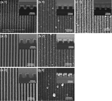
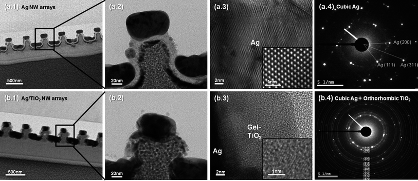
Fig. 1 and 2 show the schematic and results of the formation process of Ag/TiO2 open core–shell nanowire arrays. Facile fabrication of various geometrical configurations was enabled simply by modulating the deposition angle of the Ag thin film on the nanoimprinted UV resin template (Fig. 1b). Different evaporation angles (θ = 0°, 45° and 60°) were used for the fabrication of various Ag/TiO2 core–shell nanowires. After oblique angle deposition on the nanoimprinted UV resin patterns (Fig. 1a and b), Ag NW arrays with different step coverage profiles were fabricated (Fig. 2a.1–3). For θ = 0°, Ag thin films were deposited both on the extruded and recessed surfaces of the resin pattern while the side walls were left almost bare (Fig. 2a.1; hereafter A0). For θ = 45°, the resin was asymmetrically coated with Ag thin films on the top and side walls, due to the shadowing effect during the angled evaporation process (Fig. 2a.2; hereafter A45). For θ = 60°, Ag thin film was asymmetrically deposited on the regions close to the top surface of the resin owing to more severe shadowing effect than for θ = 45° (Fig. 2a.3; hereafter A60). All of the Ag NW arrays with different configurations (A0, A45 and A60) were coated with 50 nm thick gel-phase TiO2 thin films by an electrodeposition process (Fig. 1c). Due to the different step coverage profiles of the Ag layer in A0, A45 and A60 arrays, Ag/gel TiO2 core–shell structures with different cross-sectional shapes were fabricated (Fig. 1c.1–3 and 2b.1–3; Hereafter A0/TiO2 NW, A45/TiO2 NW and A60/TiO2 NW arrays).A0/TiO2 NW arrays were further transformed into A0/anatase TiO2 NW after a thermal annealing process (Fig. 2c.1). In case of the A0/TiO2 NW array, a TiO2 thin film completely covers the UV resin with a symmetrical profile. This configuration enables strong physical binding between the resin, Ag and TiO2 layers, and therefore the geometry of the NW array is maintained even after the thermal annealing process at temperatures higher than the decomposition temperature of the underlying UV resin. High resolution TEM images of the fabricated samples were taken to characterize the composition and crystallinity of the samples. First, the TEM images of A0 NW arrays are depicted in Fig. 3a. Well-aligned Ag NWs with 50 nm thickness on the nanoimprinted resin are observed in Fig. 3a.1 and 2. The lattice spacing is 0.235 nm (Fig. 3a.3), which can be indexed to that of the face centered cubic (fcc) Ag [*JCPDS File no. 04-0783 from ASTM]. Also, no considerable amount of silver oxide can be observed on the surface of Ag. The SAED pattern in Fig. 3a.4 shows distinct spot patterns, indicating the crystalline phases of Ag. Second, the TEM images of A0/TiO2 NW arrays are displayed in Fig. 3b. Well-aligned open core–shell NWs on the nanoimprinted resin and clear interface between the Ag and gel-TiO2 layers are observed in the TEM images (Fig. 3b.1 and 2). Also, a mixture of gel and crystalline phases is shown in the electrodeposited TiO2 thin film (Fig. 3b.3). The SAED pattern of A0/TiO2 NW in Fig. 3b.4 shows both dot and ring patterns for the cubic Ag (white ring) and orthorhombic TiO2 (blue ring). Here, the blue ring patterns represent the nanocrystalline phases of the TiO2 thin film that were formed by the partial conversion from the hydroxides (Ti(OH)4) in the gel phase to nanocrystalline TiO2 during the electrodeposition process (see the eqn (1)–(3) in the ESI†).
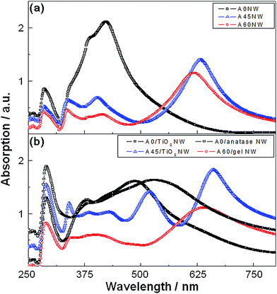
Fig. 4 shows the transverse magnetic (TM) mode optical absorbance spectra of the nanowire arrays fabricated in our study. The panels (a) and (b) present the results for the Ag and Ag/TiO2 core–shell nanowire arrays, respectively.
In each panel, multiple spectra for the structures made by different deposition angles (θ = 0°, 45° and 60°) of the Ag layer are displayed. Here, the background effect of the substrate was eliminated by the subtraction of the absorbance of the substrate. The TM mode absorption of A0 NW (Fig. 4a, black line with square dots) shows a peak at λ = 286 nm and another peak at λ = 423 nm with maximum absorbance, which are caused by the LSPR behavior of the periodic Ag NW arrays.
The TE mode absorption spectrum of Ag NW shows a peak at λ = 287 nm, which corresponds to the resonance characteristics of the Ag thin film (see the black line with square dots and the black dotted line in Fig. S3a†). As opposed to the TM mode absorption, the TE mode absorption does not exhibit a peak in the visible range and looks similar to the non-polarized absorption of the Ag thin film, since the Ag NW array structure blocks the TE mode propagation. For the same reasons, simulated TE mode absorptions of all Ag/gel TiO2 NW arrays show a similar configuration (Fig. S4†) with measured TE mode absorptions (Fig. S3†) and non-polarized absorption of the Ag thin film. By coating A0 NW with a layer of a gel-phase of TiO2, the peak at λ = 286 nm shifts to λ = 290 nm and the peak at λ = 423 nm broadens with a peak shift to λ = 487 nm (Fig. 4b, black line with square dots). This red-shift can be observed throughout the entire range of wavelengths and can be attributed to the TiO2 layer on the periodic Ag NWs.16,26 The peaks of the Ag/TiO2 NW array further shift to λ = 291 nm and λ = 529 nm after the annealing process (Fig. 4b, gray line with square dots), which is caused by the change of the refractive index of the TiO2 layer by the conversion to an anatase phase. The TM mode absorption of A45 NW (Fig. 4a, blue line with triangular dots) presents a peak at λ = 285 nm and three other peaks corresponding to the LSPR phenomena. Similar to the above-mentioned case of A0 NW, the deposition of a gel-phase TiO2 layer on the surface of the A45 NW array causes a red-shift and higher absorption (Fig. 4b, blue line with triangular dots). Similar trends of the TM mode absorption spectra (Fig. 4a–b, red lines with circular dots) can be observed for A60 NW and A60/gel NW array structures after coating with a gel–TiO2 layer on the surface of the A60 NW array.
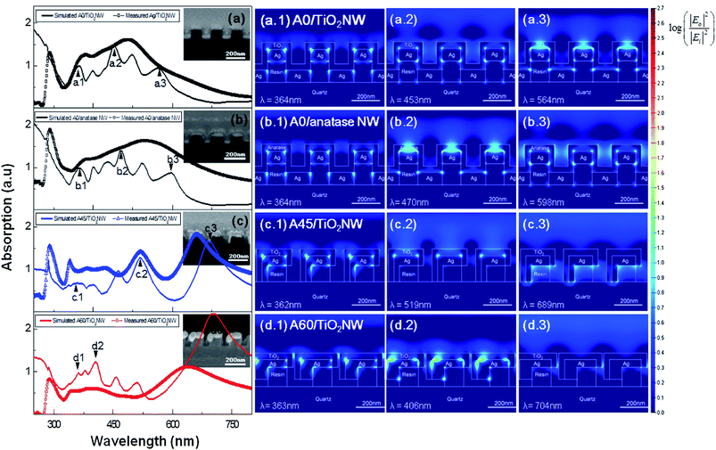
The LSPR phenomena of Ag/TiO2 core–shell nanowire arrays can be verified by a numerical simulation based on a two-dimensional finite difference time domain (FDTD) method, as shown in Fig. 5. The details of the FDTD simulation are explained in the ESI.†
Figure panels 5a show the simulated and measured TM mode absorption spectra of A0/TiO2 NW arrays. Here, the simulated TM mode absorption curve shows sharper peaks as compared to the measured values, because the geometrical models for the simulation possess sharp corners, flat-topped surfaces and straight edges, whereas the real specimens do not. Nevertheless, similar tendencies of spectral absorbance are observed between the simulated and experimental results. The LSPR behaviors are observed on the simulated TM mode absorptions of all Ag/TiO2 core–shell NW array structures, regardless of the deposition angles. Simulated TM mode absorption of A0/TiO2 NW array (Fig. 5a, black solid line) shows 5 peaks between λ = 365 nm and λ = 564 nm. The highest peak appeared at λ = 453 nm and LSPR behavior was not observed in the long wavelength region (λ > 600 nm). This simulation result shows a similar trend to the measurement data, in which several peaks exist between λ = 379 nm and λ = 487 nm and the absorption decreases over λ = 600 nm (Fig. 5a, black line with square dots). The TM mode absorption of the A0/anatase NW structure shows similar behavior to the A0/gel NW, possessing several plasmonic resonances between λ = 300 nm and λ = 600 nm. However, slightly broader and more peaks are observed for the A0/anatase NW structure (Fig. 5b, gray solid line with square dots), which seems to be caused by the change of optical properties (i.e. refractive index and extinction coefficient) during the conversion from the gel-phase to the anatase-phase of TiO2.
Figure panels 5a.1–3 and 5b.1–3 show the numerically calculated electric field distribution of the A0/gel NW and A0/anatase NW array structures. Fig. 5a.1–3 shows that the enhancement of electric field occurs at the corners of the Ag–TiO2 interface for the absorbance peaks due to the LSPR phenomena of the A0 NW array. Similar behaviors are observed for the A0/anatase NW arrays (Fig. 5b.1–3). This enhanced electric field at the Ag–TiO2 interface is beneficial for the plasmonic photocatalytic activities due to the enhanced generation of electron–hole pairs. Therefore, the Ag–TiO2 core–shell NW array structure is advantageous for the enhancement of the photocatalytic activities by the LSPR phenomena occurring near the surface reaction sites.
The simulated TM mode absorption of the A45/TiO2 NW array (Fig. 5c, blue solid line) shows several peaks between λ = 362 nm and λ = 689 nm. Also, the absorption peak values are increased at longer wavelength, which is a similar trend to the experimentally measured absorption (Fig. 5c, blue line with triangular dots). These resonance peaks of the A45/TiO2 NW array are also caused by the LSPR effect at multiple corners, as observed in the strongly localized electric field distributions in Fig. 5c.1–3. The A60/TiO2 NW array structure also shows the absorption peaks between λ = 363 nm and λ = 704 nm (Fig. 5d, red solid line), with the highest peak at λ = 704 nm. Both the A45/TiO2 NW and A60/TiO2 NW array show lower optical absorbance than A0/TiO2 NW in the low wavelength regions (300 nm < λ < 600 nm), whereas they exhibit higher absorbance in the longer wavelength regions (λ > 600 nm). The simulation was conducted for periodic nanowires (A0/TiO2 NW, A0/anatase NW, A45/TiO2 NW, and A60/TiO2 NW arrays).
In the longer wavelength regions, the electric field enhancement by the LSPR effect occurs at the interface between the Ag layer and nanoimprint resin, not at the interface between the Ag and TiO2 layers (Figure panels 5c.3 and 5d.3). Therefore, we can expect that the photocatalytic efficiencies of A45/TiO2 NW and A60/TiO2 NW arrays are lower than those of A0/TiO2 NW arrays.
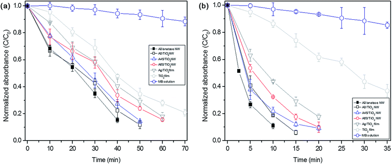
The improvement of the photocatalytic reaction of Ag/TiO2 core–shell nanostructure arrays by their enhanced optical absorption based on the LSPR phenomena was confirmed by experiment. Fig. 6a shows the normalized absorbance of methylene blue (MB) solution at λ = 660 nm after 0–1 hour of UV light exposure on different samples. Three important facts could be found from this experiment. First, the conjugation of Ag with an TiO2 thin film shows an improvement of photocatalytic reaction. The normalized absorbances (C/C0) of the MB solution after 60 min of UV exposure are 0.28 and 0.18 for gel TiO2 thin films and Ag/gel TiO2 dual layer thin films respectively. As mentioned above, this phenomenon can be explained by the enhanced electron capture and supply of holes to the TiO2 thin film at the Ag–TiO2 Schottky junction that causes an increase of superoxide radical and enhanced photocatalytic activity.9,11 Second, Ag–TiO2 core–shell nanostructuring provides a higher photocatalytic reactivity than flat Ag–TiO2 dual layer thin film structures. In particular, the A0/TiO2 NW array structure exhibits the highest photocatalytic decomposition efficiency. The normalized absorbance of the MB solution is C/C0 = 0.12 after 50 min of UV exposure for this sample. This improved photocatalytic efficiency can be attributed to the enhanced optical absorption of the A0/TiO2 NW array and the improved LSPR effect at the Ag–TiO2 interface. The A45/TiO2 NW and A60/TiO2 NW arrays show relatively higher C/C0 values than the A0/TiO2 NW array due to weaker LSPR effect and less optical absorbance in the UV spectra region as shown in Fig. 4 and 5. Third, the A0/anatase TiO2 NW shows better photocatalytic reactivity than the A0/gel TiO2 NW. The normalized absorbances (C/C0) of the MB solution after 40 min of UV exposure are 0.22 and 0.15 for A0/gel TiO2 NW and A0/anatase TiO2 NW, respectively. This can be attributed to the conduction band position (−0.2 V)25 of the anatase-phase TiO2, which is more adequate for the reduction of superoxide (O2−).
Fig. 6b shows the normalized absorbance of the MB solution at λ = 660 nm after 0–40 min of visible light exposure. Similar to ultraviolet irradiation, self-photosensitization of MB caused its decomposition under visible light without any photocatalyst. Also, the photocatalytic decomposition of MB on the gel–TiO2 thin film was observed due to the ultraviolet light (380 nm ≤ λ ≤ 400 nm) that could transmit through the visible light filter. All Ag conjugated samples show similar tendencies in the results for the above-mentioned UV exposure experiment. However, Ag/TiO2 films and Ag/TiO2 NWs show higher photocatalytic activities in visible light than in UV light since radical generation is enhanced by the electron diffusion from Ag to the TiO2 shell under visible light.16,26 Also, the Ag/TiO2 NWs show higher photocatalytic behavior than the Ag/TiO2 dual layer film due to the strong LSPR behavior of periodic metal NW arrays. In particular, the A0/anatase TiO2 NW array and A0/TiO2 NW structure exhibit the highest photocatalytic decomposition efficiency in visible light. The decomposition of MB solution on the surface of A0/TiO2 NW and A0/anatase NW samples is almost completed within 15 min of exposure. These enhanced photocatalytic efficiencies can be attributed to the strong optical absorption and improved LSPR effect at the Ag–TiO2 NW interface in the visible spectra region, as shown in Fig. 4 and 5.
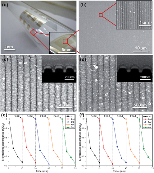
Metal-nanostructure embedded photocatalytic structures on flexible polymer substrates are drawing great attention due to their mechanical flexibility, light weight, and impact resistance.10,27 In particular, mechanically flexible polymer substrates can be installed on various objects with curved topologies, which allow their widespread application in the automotive, construction, and houseware industries. We have demonstrated the fabrication of Ag/TiO2 open core–shell nanostructure arrays on a flexible PET (polyethylene terephthalate) film. We verified the applicability of this technology to the flexible polymer substrates with a photocatalysis-based self-cleaning function and also confirmed their outstanding mechanical robustness. In particular, we fabricated an A0/gel NW array on the PET substrate as shown in Fig. 7. The A0/gel NW array could be fabricated with the same geometry, dimensions and surface morphology in a large area of PET substrate (see Fig. 7a and b). The photocatalytic performance of the A0/gel NW array on the PET substrate was found to be similar to that of the A0/gel NW array on the quartz substrate as shown in Fig. 7e and 6b. Furthermore, high mechanical compliance and ductility of the gel phase TiO2 facilitates the superior bendability and adhesion properties of the flexible substrate.10,28 This could be experimentally verified by a cyclic bending test, as shown in Fig. 7c and d. The A0/gel NW array could maintain its geometry and microstructure after 10![[thin space (1/6-em)]](https://www.rsc.org/images/entities/char_2009.gif) 000 cycles of bending with a radius of curvature of 1 cm. Figure panels 7e and f present the absorbance of MB solution during five repeated photocatalytic decolorization tests with the same A0/TiO2 NW array sample before and after 10
000 cycles of bending with a radius of curvature of 1 cm. Figure panels 7e and f present the absorbance of MB solution during five repeated photocatalytic decolorization tests with the same A0/TiO2 NW array sample before and after 10![[thin space (1/6-em)]](https://www.rsc.org/images/entities/char_2009.gif) 000 cycles of bending, respectively. We can observe that the photocatalytic activities for each test cycle are almost identical, without performance degradation due to repeated bending of the substrate. This result proves that the A0/TiO2 NW array structure can be repeatedly used for the photocatalytic decomposition of organic contaminants by multiple cycles even under mechanical bending conditions. Even though the Ag/TiO2 core–shell nanostructure showed reproducible photocatalytic activity under repeated reactions and mechanical loading cycles in our studies, oxidation of Ag in Ag/TiO2 core–shell structures is expected not only by the formation of native oxide in the initial stage17 but also by the photo-oxidation of Ag during visible light irradiation.29 In our future study, the Au-coated Ag nanowire array or Au nanowire array will be investigated as an alternative to Ag nanowire arrays for the prevention of oxidation and for long term photocatalytic stability.
000 cycles of bending, respectively. We can observe that the photocatalytic activities for each test cycle are almost identical, without performance degradation due to repeated bending of the substrate. This result proves that the A0/TiO2 NW array structure can be repeatedly used for the photocatalytic decomposition of organic contaminants by multiple cycles even under mechanical bending conditions. Even though the Ag/TiO2 core–shell nanostructure showed reproducible photocatalytic activity under repeated reactions and mechanical loading cycles in our studies, oxidation of Ag in Ag/TiO2 core–shell structures is expected not only by the formation of native oxide in the initial stage17 but also by the photo-oxidation of Ag during visible light irradiation.29 In our future study, the Au-coated Ag nanowire array or Au nanowire array will be investigated as an alternative to Ag nanowire arrays for the prevention of oxidation and for long term photocatalytic stability.
4 Conclusions
In summary, Ag/TiO2 open core–shell nanowire arrays with various geometries and plasmonic effects were fabricated by a simple manufacturing method based on nanoimprinting, oblique angle deposition, and electrodeposition. The geometrical configuration could be easily controlled into various Ag nanowire arrays simply by modulating the deposition angle of the Ag layer. The resultant periodic nanostructures exhibited strong surface plasmonic phenomena at the Ag–TiO2 interface and this provided an enhanced photocatalytic effect on the surface of TiO2 layer. We have verified experimentally that the Ag/TiO2 open core–shell nanowire array structure provides a superior photocatalytic performance to pristine TiO2 thin films or Ag/TiO2 dual-layer thin-film structures. The structural stability and reproducibility of the photocatalytic performances of the Ag/TiO2 core–shell nanostructure array were also confirmed. Finally, we have successfully demonstrated Ag/TiO2 open core–shell nanostructure arrays with good photocatalytic performance and mechanical robustness on flexible polymer substrates. We believe that this technology would be very useful for the large-scale and parallel manufacturing of plasmonic functional surfaces with self-cleaning and anti-bacterial properties. Furthermore, the proposed method of creating various core–shell nanostructures are expected to be applicable not only to photocatalytic but also to a variety of optoelectronic and bio/chemical sensing applications.Acknowledgements
This research was supported by the grants from the Basic Science Research Program (2013006809) and the Global Frontier R&D Program (2011-0031563) funded by the National Research Foundation (NRF) under the Ministry of Science, ICT and Future Planning of Korea. This work was also supported by a National Platform Technology Grant (10033636) from the Ministry of Trade, Industry and Energy of Korea.Notes and references
- H. Y. Chuang and D. H. Chen, Nanotechnology, 2009, 20, 105704 CrossRef PubMed.
- J. C. Ireland, P. Klostermann, E. W. Rice and R. M. Clark, Appl. Environ. Microbiol., 1993, 59, 1668–1670 CAS.
- F. Wu, X. Y. Hu, J. Fan, E. Z. Liu, T. Sun, L. M. Kang, W. Q. Hou, C. J. Zhu and H. C. Liu, Plasmonics, 2012, 8, 501–508 CrossRef.
- A. Orendorz, A. Brodyanski, J. Losch, L. H. Bai, Z. H. Chen, Y. K. Le, C. Ziegler and H. Gnaser, Surf. Sci., 2007, 601, 4390–4394 CrossRef CAS PubMed.
- L. Zhao, Q. Jiang and J. Lian, Appl. Surf. Sci., 2008, 254, 4620–4625 CrossRef CAS PubMed.
- C. G. Wu, C. C. Chao and F. T. Kuo, Catal. Today, 2004, 97, 103–112 CrossRef CAS PubMed.
- M. A. Behnajady, N. Modirshahla, M. Shokri and B. Rad, Global Nest J., 2008, 10, 1–7 Search PubMed.
- A. Primo, A. Corma and H. Garcia, Phys. Chem. Chem. Phys., 2011, 13, 886–910 RSC.
- X. L. He, Y. Y. Cai, H. M. Zhang and C. H. Liang, J. Mater. Chem., 2011, 21, 475–480 RSC.
- P. Wang, B. B. Huang, Y. Dai and M. H. Whangbo, Phys. Chem. Chem. Phys., 2012, 14, 9813–9825 RSC.
- B. Cheng, Y. Le and J. G. Yu, J. Hazard. Mater., 2010, 177, 971–977 CrossRef CAS PubMed.
- S. Sakthivel, M. V. Shankar, M. Palanichamy, B. Arabindoo, D. W. Bahnemann and V. Murugesan, Water Res., 2004, 38, 3001–3008 CrossRef CAS PubMed.
- Y. Tian and T. Tatsuma, J. Am. Chem. Soc., 2005, 127, 7632–7637 CrossRef CAS PubMed.
- Z. W. Liu, W. B. Hou, P. Pavaskar, M. Aykol and S. B. Cronin, Nano Lett., 2011, 11, 1111–1116 CrossRef CAS PubMed.
- Z. K. Zheng, B. B. Huang, X. Y. Qin, X. Y. Zhang, Y. Dai and M. H. Whangbo, J. Mater. Chem., 2011, 21, 9079–9087 RSC.
- R. C. Adochite, M. Torrell, L. Cunha, E. Alves, N. P. Barradas, A. Cavaleiro, J. P. Riviere, D. Eyidi and F. Vaz, J. Optoelectron. Adv. Mater., 2011, 5, 73–79 CAS.
- K. Awazu, M. Fujimaki, C. Rockstuhl, J. Tominaga, H. Murakami, Y. Ohki, N. Yoshida and T. Watanabe, J. Am. Chem. Soc., 2008, 130, 1676–1680 CrossRef CAS PubMed.
- J. G. Yu, G. P. Dai and B. B. Huang, J. Phys. Chem. C, 2009, 113, 16394–16401 CAS.
- S. H. Kim, J. D. Park and K. D. Lee, Nanotechnology, 2006, 17, 4436–4438 CrossRef CAS.
- Y. T. Pang, G. W. Meng, Y. Zhang, Q. Fang and L. D. Zhang, Appl. Phys. A: Mater. Sci. Process., 2003, 76, 533–536 CrossRef CAS PubMed.
- M. G. Kang and L. J. Guo, Adv. Mater., 2007, 19, 1391–1396 CrossRef CAS.
- K. P. Xie, Q. Wu, Y. Y. Wang, W. X. Guo, M. Y. Wang, L. Sun and C. J. Lin, Electrochem. Commun., 2011, 13, 1469–1472 CrossRef CAS PubMed.
- N. Zhou, L. Polavarapu, N. Y. Gao, Y. L. Pan, P. Y. Yuan, Q. Wang and Q. H. Xu, Nanoscale, 2013, 5, 4236–4241 RSC.
- K. Robbie, J. C. Sit and M. J. Brett, J. Vac. Sci. Technol., B, 1998, 16, 1115–1122 CAS.
- Y. V. Pleskov, Russ. J. Electrochem., 1999, 35, 1137–1138 Search PubMed.
- T. Hirakawa and P. V. Kamat, J. Am. Chem. Soc., 2005, 127, 3928–3934 CrossRef CAS PubMed.
- J. Jiang, H. Li and L. Z. Zhang, Chem.–Eur. J., 2012, 18, 6360–6369 CrossRef CAS PubMed.
- N. Gergel-Hackett, B. Hamadani, B. Dunlap, J. Suehle, C. Richter, C. Hacker and D. Gundlach, IEEE Electron Device Lett., 2009, 30, 706–708 CrossRef CAS.
- Y. Ohko, T. Tatsuma, T. Fujii, K. Naoi, C. Niwa, Y. Kubota and A. Fujishima, Nat. Mater., 2002, 2, 29–31 CrossRef PubMed.
Footnote |
| † Electronic supplementary information (ESI) available. See DOI: 10.1039/c3nr04388f |
| This journal is © The Royal Society of Chemistry 2014 |

