Scalable, flexible and high resolution patterning of CVD graphene†
Mario
Hofmann
*a,
Ya-Ping
Hsieh
*b,
Allen L.
Hsu
c and
Jing
Kong
*d
aDepartment of Material Science and Engineering, National Cheng Kung University, Tainan, 70101, Taiwan. E-mail: mario@mail.ncku.edu.tw; Fax: +886 06-2346290; Tel: +886 06-2757575
bGraduate of Institute of Opto-Mechatronics, National Chung Cheng University, Chia-yi, 62102, Taiwan. E-mail: yapinglab@gmail.com; Fax: +886 05-2724036; Tel: +886 05-2724035
cDepartment of Material Science and Engineering, National Cheng Kung University, Tainan, 70101, Taiwan. E-mail: allenhsu@mit.edu; Fax: +886 06-2346290; Tel: +886 06-2757575
dDepartment of Electrical Engineering, Massachusetts Institute of Technology, Cambridge, MA 20139, USA. E-mail: jingkong@mit.edu; Fax: +1 (617)324-5293; Tel: +1 (617)324-4068
First published on 25th October 2013
Abstract
The unique properties of graphene make it a promising material for interconnects in flexible and transparent electronics. To increase the commercial impact of graphene in those applications, a scalable and economical method for producing graphene patterns is required. The direct synthesis of graphene from an area-selectively passivated catalyst substrate can generate patterned graphene of high quality. We here present a solution-based method for producing patterned passivation layers. Various deposition methods such as ink-jet deposition and microcontact printing were explored, that can satisfy application demands for low cost, high resolution and scalable production of patterned graphene. The demonstrated high quality and nanometer precision of grown graphene establishes the potential of this synthesis approach for future commercial applications of graphene. Finally, the ability to transfer high resolution graphene patterns onto complex three-dimensional surfaces affords the vision of graphene-based interconnects in novel electronics.
Introduction
Graphene, a mono-atomic sheet of graphite, represents a new class of two-dimensional materials with properties that enable a variety of novel applications. Market predictions emphasize the use of graphene in electrode applications as the application with the largest immediate commercial impact.1 Strong competition from mature technologies, lower performance than traditional transparent conducting oxides, and requirements on processing infrastructure put the success of graphene as large scale electrodes for solar cells or traditional displays in question.2,3Graphene's high electrical conductivity considering its atomic thickness, mechanical strength, and its ability to conform to structured surfaces, however, suggest the material's potential as interconnects, in novel application such as flexible circuits,4 wearable electronics5 or novel displays.6
Competition from 1D conductors, such as nanowires and nanotubes, on the other hand, mean that additional advantages for use of graphene have to be identified, to improve the commercial appeal of this material. One such advantage is the ability to pattern graphene to expose non-conductive regions that can be used to define interconnects, transistor channels, or device terminals. High quality graphene devices with sub-micrometer resolution are routinely fabricated – a feat that is very challenging for films of 1D conductors.7
Common graphene patterning techniques, however, cannot exploit this inherent advantage of 2D materials in practical applications. Currently the fabrication of graphene patterns involves processes that can be categorized as mask lithography,8 transfer printing9 or direct patterning10,11 of graphene after it has been transferred to the target substrate. These methods suffer from a variety of disadvantages such as lacking scalability, constraints on the target substrate or fabrication speed. Furthermore, methods to pattern the catalyst before growth have only yielded low resolution features.12
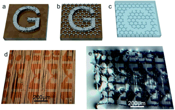
Several groups13–15 including our own, have recently devised methods to directly synthesize patterned graphene by barrier guided chemical vapor deposition (CVD) growth. The methods rely on the passivation of defined areas of catalyst material and the subsequent selective growth of graphene in the unpassivated regions (Fig. 1). This approach is expected to be compatible with a wide selection of two-dimensional materials synthesized by surface-catalytic CVD processes, such as BN16 or MoS2.
The demonstrated ability of barrier guided CVD to generate high quality graphene on pre-patterned substrates opens up the possibility to efficiently produce novel interconnects for use in wearable or flexible electronics.
Despite these advantages, there are obstacles of the barrier guided growth of graphene patterns for use in those applications. Currently, photolithography is employed to deposit barriers which is too cost and labor intensive to be considered outside of prototype fabrication. Especially wearable and flexible electronics have requirements that are different from traditional electronic devices. A significantly larger amount of interconnects will be needed to connect distributed semiconductor segments that represent the active electronic components. Therefore, the economical and scalable production of those novel interconnects is of increased significance.
We here present a new approach to form the passivation layer on a catalyst material which is compatible with a wide variety of deposition techniques. This method can satisfy demands for low cost, large scale and high resolution and can improve the practical applicability of graphene in electronic interconnects.
Methods
Graphene was synthesized by chemical vapor deposition as previously reported17 using copper as the catalyst material. Briefly, under low pressure (400 mTorr) a piece of copper foil (Alfa 13382) was annealed in hydrogen at 1000 °C for 30 minutes before methane gas was introduced to initiate the graphene growth. After 60 minute growth duration, the substrate was cooled down under a flow of hydrogen. Thus grown graphene was transferred onto substrates following a previously reported procedure.12 (More information on the patterning procedures are given in the ESI.†)Results
We chose a solution-based approach to deposit the passivation layer because of its low cost and compatibility with scalable deposition methods. We here employ an aluminum salt (AlCl3) as the precursor for the passivation layer. In contact with ambient humidity and air, the deposited material forms an aluminum hydroxide and under subsequent heating forms aluminum oxide which acts as the passivation layer. This method is not only significantly easier than previous sputtering and thermal evaporation procedures, it is also compatible with a wide variety of deposition processes that are comprehensive in scale and resolution, which is demonstrated subsequently.To accommodate demands for large area pattern generation, low cost, and production scalability, we used ink jet deposition of the passivation layer in a first set of experiments. This process is based on the area selective deposition of liquid droplets and requires no mask. Consequently, contamination of the catalyst surface through photoresist can be avoided. Furthermore, ink-jet deposition uses the precursor material more efficiently than other techniques since it produces less waste.
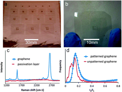
In our experiments, an aqueous solution of aluminum chloride (AlCl3) was loaded in a commercial ink-jet printer and deposited onto the copper foil. Medium resolution features can be printed using this approach on large scale samples and Fig. 2a shows a letter sized piece of Cu foil (200 × 270 mm) with aluminum precursor patterns. The maximum graphene size obtained from the patterned Cu-foil is only limited by the dimensions of the CVD chamber, which is 1′′ in our experiments. After growth, the patterned graphene could be transferred to other substrates, such as flexible polyethylene terephthalate (PET) (Fig. 2b).
Raman analysis of thus synthesized patterns reveals that the passivation layer efficiently suppresses graphene nucleation as demonstrated by the absence of carbon related Raman features inside the passivated regions (Fig. 2c). We furthermore compare the quality of the patterned graphene to graphene synthesized by traditional CVD methods. For this, the defect related ID/IG ratio18 of 10![[thin space (1/6-em)]](https://www.rsc.org/images/entities/char_2009.gif) 000 individual spectra obtained from patterned and pristine graphene was compared (Fig. 2d). The average ID/IG ratio of both samples is very similar which confirms that the quality of graphene does not deteriorate through barrier guided growth.
000 individual spectra obtained from patterned and pristine graphene was compared (Fig. 2d). The average ID/IG ratio of both samples is very similar which confirms that the quality of graphene does not deteriorate through barrier guided growth.
The absence of conductive pathways and the large band gap of the alumina result in a large resistance (>1 MΩ) of the passivation layer that can be used to isolate graphene areas from one another. This property allows the formation of extended circuits where the passivation layer is used as the dielectric support for active elements and the graphene represents the interconnect layer. The resulting ability to fabricate transparent and flexible circuits is demonstrated in Fig. 2b.
Non-traditional methods readily lend themselves to the deposition of liquid precursors over large areas at high resolution.19 One such method is the use of microcontact printing which has been used to produce nanometer sized features over square inch scales.19 Furthermore, the high achievable throughput and long life span of stamps make this technique ideally suitable for large scale production of patterned graphene.
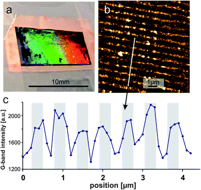
We here use a patterned stamp to deposit parallel strips of nanometer sized Al2O3 barriers as shown in Fig. 3. For this, a polydimethylsiloxane (PDMS) replica of a grating with 700 nm pitch was inked with a solution of AlCl3 and then pressed onto Cu-foil.
This presence of large arrays of nanometer-sized Al2O3 strips results in a light diffraction effect which confirms the quality of the procedure (Fig. 3a). The thus prepared substrate was subjected to CVD growth and subsequently transferred to a SiO2 sample. The formation of graphene between the Al2O3 strips was first inferred from wrinkles observed by AFM imaging (Fig. 3b). Raman analysis was then conducted to confirm the presence and quality of graphene grown. Similar to the ink-jet printed samples, the graphene quality is comparable to graphene synthesized on pristine Cu foil. Micro-Raman mapping revealed a periodic variation of the intensity of the Raman features as shown in Fig. 3c. The absence of a clear separation between graphene regions and empty barrier regions is due to the similar dimensions of the laser spot size and the graphene feature size. Consequently, a deconvolution of the laser profile has to be performed. Assuming a Gaussian intensity profile of a 1 μm laser spot, we estimate the width of the graphene strips has to be approximately 350 nm to generate the observed Raman line profile. This dimension agrees with AFM measurements of exposed Cu regions with a width of approximately 300 nm.
The high achievable resolution with simple fabrication processes highlights the potential of cheaply and scalably producing nanometer sized graphene structures with resolutions beyond the capabilities of optical lithography. This ability is expected to not only improve the usefulness of graphene interconnects but also enable new applications that can exploit size-dependent effects, i.e. quantum dots or nanoribbons for application in opto-electronic devices. The presented approach to generate high quality graphene patterns by different methods that are complementary in resolution and cost will increase the commercial appeal of graphene based devices.
We now demonstrate the potential of the presented approach for the use of graphene in non-planar devices – a novel application of the material. One of graphene's unique properties, brought about by its atomic thickness, is the ability to conform perfectly to rough surfaces. This property could prove useful in fields such as three-dimensional electronics, novel detectors,20 implantable devices20 or displays.4 Conventional lithographical techniques, however, can only produce graphene patterns on flat substrates, due to a limited depth of focus of the optical exposure units, handling issues, etc. Thus, non-planar substrates are not accessible for high resolution lithographical patterning. The described direct synthesis technique does not face these limitations since graphene patterning is accomplished on a planar substrate before growth. We here demonstrate that the usually required transfer step that is used to remove the catalytic growth substrate12 can impart new functionality. Previous reports showed that graphene can be placed onto arbitrary surfaces12 and we extend this idea by transferring pre-patterned graphene circuits onto complex shaped substrates as demonstrated in Fig. 4.
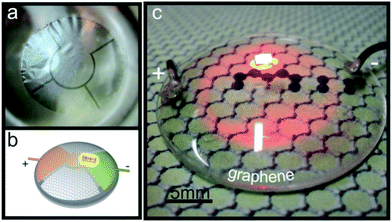
As a proof of concept, a circuit with 4 clover-leaf-shaped graphene electrodes separated by an Al2O3 barrier was produced through barrier guided growth. A thin polymer membrane was then deposited onto the patterned graphene to support it during the wet-chemical removal of the Cu substrate (Fig. 4a) shows the floating graphene/polymer membrane. The membrane was then deposited onto a glass lens and the polymer support was removed. This structure can be used as a simple electrical circuit as shown in Fig. 4b where current is directed through the graphene into a light emitting diode that was attached onto the graphene layer (Fig. 4c). This integration of commercially available electronics components into graphene circuits is intended to show their synergy and the potential for more complex circuits.
The described technique is also capable of producing high resolution features on highly complex non-planar substrates. To prove this ability, micrometer resolution patterns were generated on Cu-foil by lithographically preparing a mask on the substrate and blanket deposition of the passivation layer. After growth, the obtained graphene patterns (Fig. 1d) were released from the Cu substrate (Fig. 1e) and transferred onto a 3 millimeter diameter glass toroid. This structure represents one of the most challenging surfaces since it exhibits concave and convex surfaces of different curvatures. After removal of the polymer support, the patterned graphene conforms well to the surface with few imperfections (Fig. 5). Scanning electron microscopy confirms that the generated micrometer sized gaps and channels were still intact after transfer (inset of Fig. 5). Furthermore, the simultaneously transferred Al2O3 barrier does not exhibit cracks which is attributed to its low thickness. We therefore envision the fabrication of complete circuits on Cu-substrate and the subsequent transfer onto complex surfaces, which opens up new ways to integrate electronics for a variety of applications, such as implantable devices, bio-inspired circuits, three-dimensional electronics, etc.
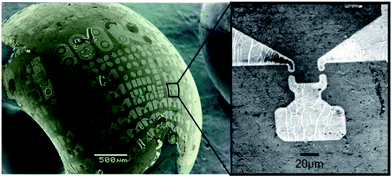 | ||
| Fig. 5 False-color SEM image of lithographically patterned graphene transferred onto a 3 mm glass torus, (inset) magnification of feature with 5 μm gap feature. | ||
Conclusions
In conclusion, the scalable and high quality fabrication of graphene patterns using a barrier guided CVD method is reported. Using a solution based approach we produce large area and high resolution passivation features that restrict the graphene growth to certain areas. Several approaches to depositing the patterned passivation layer were demonstrated that are complementary in resolution, scale and cost. Finally, the deposition of pre-patterned graphene onto non-planar substrates was shown and the ability to generate high resolution graphene patterns on complex surfaces opens up novel application areas for electronic devices.Acknowledgements
M. Hofmann acknowledges support under NSC-101-2112-M-006-017-MY3 and D102-33B07. Y. P. Hsieh acknowledges support under NSC-100-2112-M-194-006-MY3. J. Kong acknowledges support under ONR MURI N00014-09-1-1063.Notes and references
- IDTechEx, 2010.
- R. G. Gordon, MRS Bull., 2000, 25, 52–57 CrossRef CAS.
- S. De and J. N. Coleman, ACS Nano, 2010, 4, 2713–2720 CrossRef CAS PubMed.
- R. H. Kim, M. H. Bae, D. G. Kim, H. Cheng, B. H. Kim, D. H. Kim, M. Li, J. Wu, F. Du, H. S. Kim, S. Kim, D. Estrada, S. W. Hong, Y. Huang, E. Pop and J. A. Rogers, Nano Lett., 2011, 11, 3881–3886 CrossRef CAS PubMed.
- S. K. Lee, B. J. Kim, H. Jang, S. C. Yoon, C. Lee, B. H. Hong, J. A. Rogers, J. H. Cho and J. H. Ahn, Nano Lett., 2011, 11, 4642–4646 CrossRef CAS PubMed.
- Z. G. Wang, Y. F. Chen, P. J. Li, X. Hao, J. B. Liu, R. Huang and Y. R. Li, ACS Nano, 2011, 5, 7149–7154 CrossRef CAS PubMed.
- A. Behnam, L. Noriega, Y. Choi, Z. Wu, A. G. Rinzler and A. Ural, Appl. Phys. Lett., 2006, 89, 093107 CrossRef.
- Y. Zhou and K. P. Loh, Adv. Mater., 2010, 22, 3615–3620 CrossRef CAS PubMed.
- B. H. Hong, K. S. Kim, Y. Zhao, H. Jang, S. Y. Lee, J. M. Kim, K. S. Kim, J. H. Ahn, P. Kim and J. Y. Choi, Nature, 2009, 457, 706–710 CrossRef PubMed.
- C. M. Marcus, M. C. Lemme, D. C. Bell, J. R. Williams, L. A. Stern, B. W. H. Baugher and P. Jarillo-Herrero, ACS Nano, 2009, 3, 2674–2676 CrossRef PubMed.
- J. Liang, Y. Chen, Y. Xu, Z. Liu, L. Zhang, X. Zhao, X. Zhang, J. Tian, Y. Huang, Y. Ma and F. Li, ACS Appl. Mater. Interfaces, 2010, 2, 3310–3317 CAS.
- A. Reina, X. T. Jia, J. Ho, D. Nezich, H. B. Son, V. Bulovic, M. S. Dresselhaus and J. Kong, Nano Lett., 2009, 9, 30–35 CrossRef CAS PubMed.
- N. S. Safron, M. Kim, P. Gopalan and M. S. Arnold, Adv. Mater., 2012, 24, 1041–1045 CrossRef CAS PubMed.
- US Pat., 20120241069, 2012.
- M. Wang, L. Fu, L. Gan, C. Zhang, M. Rümmeli, A. Bachmatiuk, K. Huang, Y. Fang and Z. Liu, Sci. Rep., 2013, 3, 1238 Search PubMed.
- Z. Liu, L. Ma, G. Shi, W. Zhou, Y. Gong, S. Lei, X. Yang, J. Zhang, J. Yu, K. P. Hackenberg, A. Babakhani, J.-C. Idrobo, R. Vajtai, J. Lou and P. M. Ajayan, Nat. Nanotechnol., 2013, 8, 119–124 CrossRef CAS PubMed.
- M. Hofmann, Y. C. Shin, Y. P. Hsieh, M. S. Dresselhaus and J. Kong, Nano Res., 2012, 5, 504–511 CrossRef CAS.
- S. Bhaviripudi, X. Jia, M. S. Dresselhaus and J. Kong, Nano Lett., 2010, 10, 4128–4133 CrossRef CAS PubMed.
- Y. N. Xia and G. M. Whitesides, Annu. Rev. Mater. Sci., 1998, 28, 153–184 CrossRef CAS.
- I. W. Jung, J. L. Xiao, V. Malyarchuk, C. F. Lu, M. Li, Z. J. Liu, J. Yoon, Y. G. Huang and J. A. Rogers, Proc. Natl. Acad. Sci. U. S. A., 2011, 108, 1788–1793 CrossRef CAS PubMed.
Footnote |
| † Electronic supplementary information (ESI) available: Detailed materials characterization and experimental procedures. See DOI: 10.1039/c3nr04968j |
| This journal is © The Royal Society of Chemistry 2014 |

