Ferroelectric-gate thin-film transistors with Bi3.15Nd0.85Ti3O12 gate insulators on LaNiO3-buffered Si substrates
H. J. Songab,
T. Dingab,
X. L. Zhong*ab,
J. B. Wang*ab,
B. Liab,
Y. Zhanga,
C. B. Tanab and
Y. C. Zhoua
aSchool of Materials Science and Engineering, Xiangtan University, Xiangtan 411105, Hunan, China. E-mail: xlzhong@xtu.edu.cn; jbwang@xtu.edu.cn
bNational-Provincial Laboratory of Special Function Thin Film Materials, Xiangtan University, Xiangtan 411105, Hunan, China
First published on 7th November 2014
Abstract
Ferroelectric-gate thin-film transistors (FGTs) with a stacked oxide structure of ZnO/Bi3.15Nd0.85Ti3O12 (BNT)/LaNiO3 (LNO) on Si substrates have been prepared and characterized. The FGT devices show good electrical properties, such as a large “on” current of 2.5 × 10⁻⁴ A and low threshold voltage of 1.1 V. These are mainly attributed to the coupling enhancement of the gate electric field to the channel layer due to a-axis preferential orientation of BNT ferroelectric-gate insulator thin films obtained by using the LNO buffer layer and the relatively good interface properties. The results suggest that ZnO/BNT/LNO/Si structures are well suited for thin-film transistors for future nonvolatile memory applications.
Introduction
Ferroelectric-gate thin-film transistors (FGTs) have attracted much attention due to their simple device structure, non-destructive readout operation, low power consumption and high endurance.1–6 The various types of FGTs composed of different stacked structures have been investigated.7–13 Nevertheless, the gate insulators of most of these thin-film transistors are epitaxial ferroelectric thin films grown on special substrates (e.g., SrTiO3). The expensive substrates and the incompatibility with the well-established Si technology will hinder the progress of the FGT applications. Thus, developing Si-based thin-film transistors with high-quality ferroelectric thin films as gate insulators is important for promoting the FGT applications. Up until now, few studies have reported FGTs deposited directly on Si substrates.Ferroelectric bismuth-layer perovskite films such as SrBi2Ta2O9 (SBT) and lanthanide-doped Bi4Ti3O12 (BIT) are recognized as promising materials for FGTs applications due to their high fatigue resistance and large dielectric constant.14 As we know, while ferroelectric film has a strongly anisotropic polarization and dielectric properties. For example, the polarization of BIT is as large as 50 μC cm−2 along a-axis but rather small as 4 μC cm−2 along c-axis and the dielectric constant of the a-axis-oriented film is much larger than that of the c-axis-oriented film.15,16 In fact, unfortunately the films of these materials are easily grown with the c-axis perpendicular to the film plane (i.e., the c-axis orientation) because of the highly anisotropic structures,17 which influences the properties of corresponding devices. Therefore, in order to achieve bismuth-layered perovskite film FGTs with good performance, a-axis-oriented film with a high polarization and dielectric constant is essential. Using an appropriate buffer layer with specific orientation is a good way to grow non c-axis-oriented bismuth-layered perovskite films on Si substrates. For example, by using (110)-oriented SrRuO3 (SRO) and (100)-oriented Y2O3-stabilized ZrO2 (YSZ) buffer layers, Lee et al.17,18 have fabricated the a-axis-oriented Bi3.25La0.75Ti3O12 (BLT) films on Si (100) substrates. Perovskite LaNiO3 (LNO) not only has same chemistry structure and close crystal constant with SRO, but also has lower cost than SRO. Furthermore, LNO can act as a good electrode layer due to its low resistivity and good metallic conductivity.10,19 Therefore, in this paper we use LNO as the buffer layer and Bi3.15Nd0.85Ti3O12 (BNT) as ferroelectric-gate insulator to fabricate Si-based FGTs. The LNO layer serves as a useful metal oxide bottom electrode and at the same time forms a template to promote the a-axis preferential orientation growth of BNT films. In the study, ZnO thin films are chosen as the channel layer of FGTs because of its low cost, low photosensitivity, and high mobility.20 On the other hand, pulsed laser deposition (PLD) is a unique technique to deposit oxide thin films and multi-layered thin films. The physical properties of oxide thin films can be easily tunned by changing the experimental conditions of PLD, such as oxygen pressure.21 Meanwhile, a very clean and smooth interface can be obtained by PLD, which is specially unique to deposit oxide multi-layered thin films or devices. Therefore, PLD is chosen to deposit ZnO/BNT/LaNiO3 FGTs in this study.
Experimental
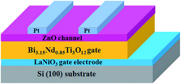
The schematic illustration of ZnO/BNT/LNO/Si FGT is shown in Fig. 1. The ZnO and BNT thin films were deposited by using a pulsed laser deposition system (PLD-5000) with KrF excimer laser (COHERENT COMPEX 205, λ = 248 nm, 20 ns pulse duration) at a substrate temperature of 400 and 700 °C, oxygen partial pressure of 10 and 200 mTorr, respectively.22 Prior to the deposition of the BNT thin films, a 50 nm thick high (110)-oriented LNO buffer/bottom electrode layer was deposited on 6° miscut Si (100) substrate by PLD. The thickness of ZnO and BNT layers is 60 and 550 nm, respectively. Source/drain Pt electrodes were deposited on the ZnO layers using the mask plates. The channel width (W) and length (L) of FGTs are 1500 and 200 μm, respectively. The structures of the films were characterized by X-ray diffraction (XRD) with Cu Kα radiation. The atomic force microscope (AFM) (Q-Scope 850) was used to characterize the surface roughness of the films. The polarization–electric field (P–E) hysteresis loops of BNT films were measured using a RT Precision Workstation ferroelectric analyzer. Transistor characteristics were measured using a semiconductor device analyzer (Agilent B1500A).Results and discussion
Fig. 2(a) and (b) are the XRD patterns of BNT thin films deposited on different electrodes, and the XRD pattern of BNT powders is shown in Fig. 2(c) for comparison. All of the XRD patterns are indexed according to the standard powder diffraction data of BIT. It is notice that the BNT films deposited on LNO electrodes show an a-axis preferential crystalline orientation, while the BNT films deposited on Pt electrodes show a c-axis preferential crystalline orientation. In order to support the claim, the degree of preferred orientation F has been calculated by using the relationship proposed by Lotgering,23,24| F(h00) = (P(h00) − P0)/(1 − P0), | (1) |
| P(h00) = ∑I(h00)/∑I(hkl), | (2) |
| P0 = ∑I*(h00)/∑I*(hkl). | (3) |
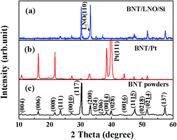 | ||
| Fig. 2 The XRD patterns of (a) the BNT thin films deposited on LNO electrodes, (b) the BNT thin films deposited on Pt electrodes, and (c) the BNT powders. | ||
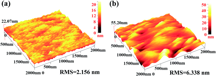
The AFM 3D images of the BNT thin films with a scanning area of 2 × 2 μm2 are shown in Fig. 3. It is found that BNT thin films deposited on LNO electrodes exhibit a smoother surface morphology than the thin films on Pt electrodes. A much smaller root-mean-square roughness (RMS) of 2.156 nm for the BNT films on LNO electrodes has been obtained, which is benefit to obtain a sharp ZnO/BNT interface in the FGTs.
Fig. 4(a) and (b) show the P–E hysteresis loops and dielectric constant εr as a function of frequency for the BNT thin films deposited on different electrodes, respectively. One can note that the thin films exhibit typical ferroelectric hysteresis loops on the condition of 10 kHz frequency. It is very clear that the ferroelectric polarization and dielectric constant of the BNT film are strongly dependent on the film orientation. The 2Pr of the a-axis preferential film on LNO electrode is much larger than that of the c-axis preferential film on Pt electrode. The dielectric constant εr = 248 at 1 MHz of the a-axis preferential film is more than twice as much that εr = 107 at 1 MHz of the c-axis preferential film. A similar observation has been reported for BNT films prepared by using CSD method.16
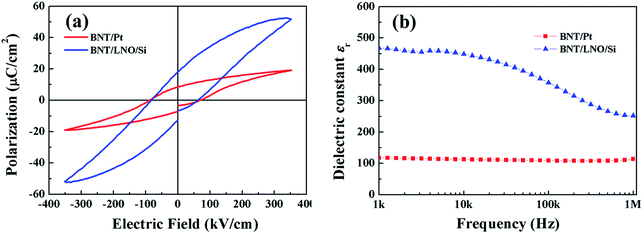 | ||
| Fig. 4 (a) P–E hysteresis loops and (b) the frequency dependence of dielectric constant of the BNT films on different electrodes. | ||
Fig. 5(a) and (b) show the drain current–drain voltage (IDS–VDS) output characteristics of ZnO/BNT/LNO/Si and ZnO/BNT/Pt FGTs at positive gate bias from 0 to 8 V, respectively. Both of transistors show the typical n-channel behavior operating in enhancement mode and clear current saturation at low drain voltage. While ZnO/BNT/LNO/Si FGTs have much larger “on” current than ZnO/BNT/Pt FGTs. A large “on” current (2.5 × 10⁻⁴ A) of ZnO/BNT/LNO/Si FGTs is observed when the gate voltage VGS = 8 V and VDS = 4 V, which is larger than that of ZnO/BNT/Pt FGTs (2.9 × 10⁻⁷ A).
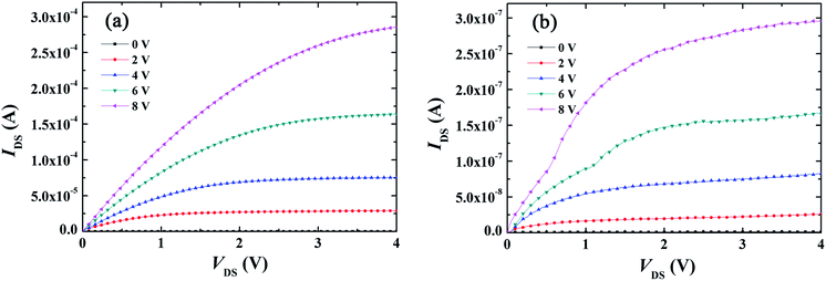 | ||
| Fig. 5 Drain current and drain voltage (IDS–VDS) characteristics of (a) ZnO/BNT/LNO/Si and (b) ZnO/BNT/Pt FGTs. | ||
Fig. 6(a) shows the IDS–VGS logarithmic transfer curve of the fabricated ZnO/BNT/LNO/Si FGTs in a double sweep mode when gate voltage sweeps from −4 to 8 V at a VDS of 0.2 V. A counterclockwise hysteresis loop as indicated by arrows is obtained owing to the ferroelectric polarization reversal of the BNT thin films from the IDS–VGS characteristics curve, which shows the fabricated device has a good nonvolatile memory function. The obtained memory window (MW) and drain-current on/off ratio are as large as about 3.0 V and 1.8 × 10⁶, respectively. Moreover, a low subthreshold voltage swing of 240 mV per decade is obtained.
The linear transfer characteristics IDS–VGS and the linear fit of IDS1/2–VGS for the ZnO/BNT/LNO/Si and ZnO/BNT/Pt FGTs are shown in Fig. 6(b) and (c). The threshold voltage (Vth) of the ZnO/BNT/LNO/Si is determined to be Vth = 1.1 V by the IDS1/2–VGS curve of the transistors operating in the saturation region, which is slightly lower than the one (Vth = 1.4 V) of the ZnO/BNT/Pt FGTs. The channel mobility (μsat) can be deduced using the equation in the saturation region for a field effect transistor.
 | (4) |
From the above results, one can see that the fabricated ZnO/BNT/LNO/Si FGTs have good electrical properties, such as large “on” current and low operating voltage. This can be explained as follows. On the one hand, a-axis preferential orientation BNT thin film obtained by using LNO buffer layer results in larger polarization and dielectric constant and thus increases the coupling of the gate electric field to the channel layer, which is very beneficial to the improvement of FGTs properties.25,26 On the other hand, it may be attributed to the relatively good interface properties between ZnO and BNT thin films owing to the smoother surface of BNT thin films on LNO buffer layer.27,28
Conclusions
In summary, the Si-based FGTs with BNT as gate dielectrics and ZnO as channel layer were fabricated and characterized. The a-axis preferential orientation BNT gate film with a smoother surface and a significant enhancement of the polarization and dielectric constant is obtained by using LNO buffer/electrode layer. ZnO/BNT/LNO/Si transistors demonstrate good operating characteristics with a large “on” current and a low threshold voltage. The subthreshold slope, memory window, and on/off ratio are measured to be 240 mV per decade, 3.0 V and 1.8 × 10⁶, respectively. The good transistor performances suggest that ZnO/BNT/LNO/Si structures are well suited for FGT application.Acknowledgements
This work was supported by the National Natural Science Foundation of China (nos 11372266, 11272274 and 11032010), the Hunan Provincial Natural Science Foundation of China (no. 12JJ1007), the Specialized Research Fund for the Doctoral Program of Higher Education (no. 20114301110004) and the Foundation for the Author of National Excellent Doctoral Dissertation of PR China (201143).Notes and references
- L. Liang, T. Fukushima, K. Nakamura, S. Uemura, T. Kamata and N. Kobayashi, J. Mater. Chem. C, 2014, 2, 879–883 RSC.
- X. Hou, Y. Xia, S. C. Ng, J. Zhang and J. S. Chang, RSC Adv., 2014, 4, 37687–37690 RSC.
- Y. Kim, L. S. O'Neil, M. Kathaperumal, L. R. Johnstone, M.-J. Pan and J. W. Perry, RSC Adv., 2014, 4, 19668–19673 RSC.
- M. Li, I. Katsouras, C. Piliego, G. Glasser, I. Lieberwirth, P. W. Blom and D. M. de Leeuw, J. Mater. Chem. C, 2013, 1, 7695–7702 RSC.
- T. T. Phan, T. Miyasako, K. Higashimine, E. Tokumitsu and T. Shimoda, Appl. Phys. A, 2013, 113, 333–338 CrossRef CAS PubMed.
- P. K. Nayak, J. Caraveo-Frescas, U. S. Bhansali and H. Alshareef, Appl. Phys. Lett., 2012, 100, 253507 CrossRef PubMed.
- H. J. Song, P. P. Liu, X. L. Zhong, B. Li, T. Chen, F. Wang, J. B. Wang and Y. C. Zhou, Appl. Phys. Lett., 2014, 105, 053506 CrossRef PubMed.
- P. Tue, T. Miyasako, E. Tokumitsu and T. Shimoda, Adv. Mater. Sci. Eng., 2013, 2013, 692469 Search PubMed.
- Y. Kaneko, H. Tanaka, M. Ueda, Y. Kato and E. Fujii, IEEE T. Electron. Dev., 2011, 58, 1311–1318 CrossRef CAS.
- T. Miyasako, B. N. Q. Trinh, M. Onoue, T. Kaneda, P. T. Tue, E. Tokumitsu and T. Shimoda, Appl. Phys. Lett., 2010, 97, 173509 CrossRef PubMed.
- T. Fukushima, T. Yoshimura, K. Masuko, K. Maeda, A. Ashida and N. Fujimura, Thin Solid Films, 2010, 518, 3026–3029 CrossRef CAS PubMed.
- D. Ito, N. Fujimura, T. Yoshimura and T. Ito, J. Appl. Phys., 2003, 93, 5563 CrossRef CAS PubMed.
- Y. Ishibashi, in Ferroelectric Thin Films, ed. M. Okuyama and Y. Ishibashi, Springer, 2005, pp. 3–23 Search PubMed.
- X. J. Lou, H. J. Zhang, Z. D. Luo, F. P. Zhang, Y. Liu, Q. D. Liu, A. P. Fang, B. Dkhil, M. Zhang, X. B. Ren and H. L. He, Appl. Phys. Lett., 2014, 105, 102907 CrossRef PubMed.
- J. B. Wang, P. J. Li and X. L. Zhong, Appl. Surf. Sci., 2011, 257, 4171–4174 CrossRef CAS PubMed.
- C. Lu, Y. Qiao, Y. Qi, X. Chen and J. Zhu, Appl. Phys. Lett., 2005, 87, 222901–222903 CrossRef PubMed.
- H. N. Lee, D. Hesse, N. Zakharov and U. Gösele, Science, 2002, 296, 2006–2009 CrossRef CAS PubMed.
- H. N. Lee, D. Hesse, N. Zakharov, S. K. Lee and U. Gosele, J. Appl. Phys., 2003, 93, 5592–5601 CrossRef CAS PubMed.
- M. Jain, B. Kang and Q. Jia, Appl. Phys. Lett., 2006, 89, 242903 CrossRef PubMed.
- H. Dong, Y. Yang and G. Yang, ACS Appl. Mater. Interfaces, 2014, 6, 3093–3098 CAS.
- Q. K. Li, J. B. Wang, B. Li, X. L. Zhong, F. Wang and C. B. Tan, Appl. Surf. Sci., 2013, 283, 623–628 CrossRef CAS PubMed.
- S. Yuan, J. Wang, X. Zhong, J. Huang and Y. Zhou, RSC Adv., 2013, 3, 24362–24366 RSC.
- F. Lotgering, J. Inorg. Nucl. Chem., 1959, 9, 113–123 CrossRef CAS.
- G. Mambrini, E. Leite, M. Escote, A. Chiquito, E. Longo, J. Varela and R. Jardim, J. Appl. Phys., 2007, 102, 043708 CrossRef PubMed.
- H. Sakai, H.-J. Cheong, T. Kodzasa, H. Tokuhisa, K. Tokoro, M. Yoshida, T. Ikoga, K. Nakamura, N. Kobayashi and S. Uemura, Jpn. J. Appl. Phys., 2014, 53, 05HB13 CrossRef.
- H. J. Song, D. Lv, J. B. Wang, B. Li, X. L. Zhong, L. H. Jia and F. Wang, RSC Adv., 2014, 4, 54924–54927 RSC.
- P. Schwinkendorf, M. Lorenz, H. Hochmuth, Z. Zhang and M. Grundmann, Phys. Status Solidi A, 2014, 211, 166–172 CrossRef CAS.
- P. V. Thanh, B. N. Q. Trinh, T. Miyasako, P. T. Tue, E. Tokumitsu and T. Shimoda, Ferroelectr., Lett. Sect., 2013, 40, 17–29 CrossRef CAS.
| This journal is © The Royal Society of Chemistry 2014 |

