Solution based, on chip direct growth of three-dimensionally wrinkled gold nanoparticles for a SERS active substrate†
Suseung
Lee‡
a,
Hyeon Don
Song‡
a,
Young In
Yang
a,
Gil-Pyo
Kim
a,
Inhee
Choi
*b and
Jongheop
Yi
*a
aInstitute of Chemical Processes, School of Chemical and Biological Engineering, College of Engineering, Seoul National University, Seoul, 151-742, Republic of Korea. E-mail: jyi@snu.ac.kr; Tel: +82-2-880-7438
bDepartment of Life Science, University of Seoul, Seoul 130-743, Republic of Korea. E-mail: inheechoi1@uos.ac.kr; Tel: +82-2-6490-2675
First published on 4th November 2014
Abstract
This work reports a solution-based method for on chip growth of wrinkled gold nanoparticles. During the growth process, time-resolved scattering profiles were measured, which permitted one to collect information regarding the growth kinetics. Finally, using the fabricated substrate, a 30 times stronger SERS enhancement was achieved than a spherical nanoparticle immobilized substrate.
Since its introduction more than 30 years ago,1 the surface-enhanced Raman scattering (SERS) technique has continued to attract attention and has been widely used as a promising analytical method in diverse fields ranging from basic science to applied engineering. Although the intensity of Raman scattering itself is too weak to measure, it can be significantly enhanced at the surface of certain types of metallic nanostructures. The explanation for this enhancement phenomenon is still a matter of controversy, but it is widely accepted that the Raman enhancement is due to two issues: electromagnetic and chemical enhancement mechanisms.2 Among them, the electromagnetic enhancement mechanism, an important contributor, is closely related to the composition, size and shape of the metallic nanostructure.
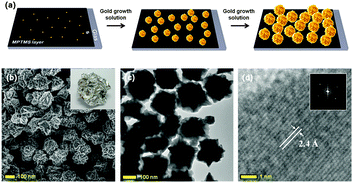
It is known that the increased local electromagnetic field around the metallic nanostructure, the so called “hot spot”, is a particularly key factor for enhancing Raman signals.3 Thus, extensive studies have been focused on the development of unique metallic nanostructures with numerous hot spots. In particular, novel metals such as gold and silver have been intensively investigated for fabricating various morphologies such as rod,4 crescent,5 star,6 flower,7 snowflake8 shapes rather than smooth spheres. These types of metallic nanostructures are usually synthesized and utilized in the form of colloidal solution. However the method has certain drawbacks, in that colloidal nanoparticles could undergo aggregation under certain solution conditions, such as pH, temperature or impurities. This unwanted aggregation results in the failure of stability and reproducibility of the signals. This being the case, synthesized nanoparticles are usually utilized in a SERS analysis after being immobilized on a substrate. Otherwise, substrates with arrayed nanoparticles are generally fabricated via complex clean room processes.9 In another approach for generating abundant hot spots, two-dimensionally wrinkled substrates were also fabricated through a shrinking process of the polymeric surface, where a metallic thin film is located.10 Since the wrinkled substrates have interstitial voids, intersections, and high radii of curvature of the structures,11 it is advantageous to generate abundant hot spots compared to other shapes. Although these approaches for enhancing SERS signals are quite efficient, they represent a bottle-neck for further applications, in that sophisticated fabrication skills, complex processes and instrumentation are still required for fabrication. Herein, we report on the development of a facile solution based method for fabricating a substrate with three-dimensionally wrinkled gold nanoparticles (WGNPs). WGNPs that are directly grown on the substrate possess a key feature that can make them suitable for SERS substrates; the roughened surface caused by the wrinkles generates enormous numbers of hot spots for localized electromagnetic field enhancement. Furthermore, they are directly synthesized on the substrate. As a result, no additional steps are needed for immobilization of the synthesized nanostructures. In this study, we immobilized small gold nanoparticles (as seeds) and directly synthesized WGNPs on the substrate using a typical seed-mediated growth method, as described in Fig. 1a. The growth procedure for the WGNPs was investigated by using Rayleigh scattering micro-spectroscopy, and correlated with Raman scattering measurements of the fabricated substrates at each condition in order to determine the optimal conditions. This series of experiments is described below.
Firstly, small sized gold nanoparticles (d ≈ 4–5 nm, see Fig. S1, ESI†) were prepared by the sodium borohydride reduction of HAuCl4, and were used as seeds for further gold nanoparticle growth. In order to immobilize the seed nanoparticles on a glass substrate, (3-mercaptopropyl)trimethoxysilane (MPTMS) was adopted for the preparation of a thiol-modified substrate where gold nanoparticles can be strongly attached. The immobilized gold seeds were then grown in an aqueous growth solution containing gold ions (from HAuCl4), a capping agent (hexadecyltrimethylammonium bromide, CTAB), a reducing agent (L-ascorbic acid) and silver nitrate (AgNO3). Ag ions are commonly used as cationic additives in the synthesis of various shaped nanoparticles12 (further experimental details can be found in supplementary methods, ESI†).
Fig. 1b shows the morphology of typical wrinkled nanoparticles obtained from field emission scanning electron microscopy (FE-SEM). Each nanoparticle possesses abundant wrinkled tips resembling a crumpled sheet of aluminium foil (inset of Fig. 1b). A high-resolution transmission electron microscopy (HR-TEM) image and a FFT (fast Fourier transform) pattern clearly indicate the sizes of nanoparticles (ca., 150–200 nm) and confirm its highly crystalline nature, respectively (Fig. 1c and d). The lattice fringes with a d-spacing value of 0.24 nm corresponds to the (111) planes of a typical face centered cubic (fcc) gold structure (inset of Fig. 1d).
The exact mechanism for the formation of wrinkled structures on the surface of gold nanoparticles is not fully understood at present, but is believed to be associated with the large amount of Ag ions that are present during the synthesis process. It is probably due to the reason that a large amount of Ag ions rapidly covers a large surface of an initial Au seed and Au ions are deposited at the uncovered small gaps. It would be a plausible explanation that the shape-directing effects are due to the underpotential deposition (UPD) of Ag on the surface of the Au particles, which have been extensively employed in synthesizing various nanocrystals.12 The preferential deposition of Ag blocks surface sites on higher energy facets, slowing the growth of the highest energy facet where Ag sufficiently covers, and ensuring that these specific facets are retained in the final Au nanostructure. Thus, the growth of Au would preferably occur on the lower energy facet. The observation of a Au(111) plane in the TEM characterization provides supporting evidence of the preferential growth direction for forming wrinkled structures. Note that the Au(111) facet is energetically favorable, since it has the lowest surface energy.13 Energy dispersive X-ray analysis (EDX) reveals that our fabricated wrinkled nanoparticle is mainly composed of Au (see Fig. S2, ESI†). However, we would like to further address that a minimal amount of Ag could exist on the surface of the wrinkled nanostructures since the UPD of Ag on Au results in a monolayer or submonolayer coverage of Ag on the surface of nanoparticles.12 Based on our observations, the concentration of silver ions causes a dramatic difference in the morphology of the nanoparticles (see Fig. S3, ESI†), as would be expected. As the concentration of Ag ions increases, the wrinkled structures become more prominent. However, the concentration of CTAB is found to be not a decisive factor for the generation of a wrinkled structure (data not shown).
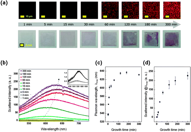
Having demonstrated that WGNPs are directly grown on the substrate, we next investigated the optical properties of the substrates prepared at each growth step in order to determine the optimal substrate for SERS enhancement. Time-resolved scattering images and corresponding spectra were recorded using a dark-field micro-spectroscopic system (Fig. 2a). The system consists of an Axio observer Z1 inverted microscope equipped with a dark-field condenser (Carl Zeiss, Germany) and a line-imaging spectrometer (Monorai320i, Dongwoo Optron Co., Korea) coupled with a 1024 × 256 pixel cooled spectrograph CCD camera (Andor Technology PLC, UK).14 In the initial stage of growth (within 5 minutes), green-colored scattering spots (see Fig. S4, ESI†) were observed, which represent a localized surface plasmon resonance (LSPR) band with a wavelength of around 560 nm (see Fig. 2b). These properties are similar to those of typical spherical gold nanoparticles. As the growth proceeds, the scattering color of the substrate gradually changed from green to red. Furthermore the number of spots and their brightness also increased significantly. Photographs of the substrates also show a dramatic color change to pink from the transparent substrate (lower panel of Fig. 2a). The LSPR bands were broadened and the LSPR wavelength (λmax) was shifted to a longer wavelength near 650 nm. This can be attributed to the increase of the size of nanoparticles and the extent of wrinkles in the nanoparticles as growth progresses. Interestingly, the LSPR wavelength (λmax) in the scattering spectra did not significantly change after 120 minutes (Fig. 2c), although the scattering intensity at λmax increased slightly up to 300 minutes (Fig. 2d). This indicates that the size growth of WGNPs is essentially terminated within 120 minutes, and the density of WGNPs on the substrate further increases afterward.
 | ||
| Fig. 2 (a) Dark-field scattering images (upper panel) and photographs (lower panel) of WGNPs immobilized on a glass substrate with respect to growth time from 1 min to 300 min; the white light illumination power was constant. Samples of 1 and 5 min are also imaged with higher illumination power since the intensity of green colored spots is relatively weak compared to the red colored spots (see Fig. S3, ESI†). (b) Rayleigh scattering spectra of WGNPs with respect to growth time, the LSPR bands were broadened and the LSPR wavelength (λmax) was shifted to a longer wavelength near 650 nm. The inset shows Rayleigh scattering spectra for 1, 3 and 5 min, showing weak intensity levels, as indicated by a yellow box. (c and d) Plots of the plasmon resonance wavelength (λmax) and the intensity at λmax as a function of growth time. | ||
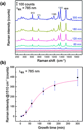
In order to investigate the applicability of the prepared substrate as a SERS substrate, the Raman signal of rhodamine 6G (R6G), a representative Raman probe molecule, was measured. The Raman spectrum was collected using a commercially available Raman spectrometer (QE65-Pro-Raman spectrometer, Ocean Optics, USA) with a coupled fiber probe. The SERS intensities of 100 μM aqueous solutions of R6G were measured as a function of the growth stage of the WGNPs (Fig. 3a). Raman intensities of all Raman shift bands increased dramatically with time of growth. This indicates that the SERS signal increment pattern is closely correlated with the increase in both plasmon wavelength and its intensity, as shown above in Fig. 2b and c. That is, we can understand that strong Raman enhancement is derived from two factors: one is the increase of the particle size and another is the generation of wrinkled structures as hot spot generators, as mentioned earlier. It should also be noted that the density of WGNPs is also an important factor for SERS signal enhancement.
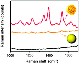
It is important to address the magnitude of SERS enhancement derived from the wrinkled structures. Compared to the substrate immobilized on spherical gold nanoparticles of a similar diameter (ca. 150 nm), our wrinkled nanoparticles' substrate showed a 30 times stronger signal intensity at 1510 cm−1 (Fig. 4). It is also noteworthy that Raman signals of R6G measured using the glass substrate without gold nanoparticles are not detectable at concentrations below 100 μM. In the case of the cleaned glass substrate, no signal was observed, even at a higher R6G concentration of 1 mM (see Fig. S5, ESI†). Raman signals at lower R6G concentrations were also measured using our fabricated substrates and showed a good linearity for concentration (see Fig. S6, ESI†).
In summary, we report on a facile solution-based method to fabricate three-dimensionally wrinkled gold nanoparticles (WGNPs) with sharp tips on the substrate. Particle growth kinetics was investigated by the time-resolved collection of scattering profiles, which can be correlated with the resulting SERS signal enhancement. The use of wrinkled nanoparticles allowed us to achieve a 30 times stronger signal enhancement compared to spherical nanoparticles in SERS measurements. We expect that the presented on chip direct growth method could be easily integrated for development of sensor chips to improve the sensitivity in other optical sensing applications as well as Raman spectroscopy.
This work was supported by the Seoul National University Research Grant. This research was also supported by Basic Science Research Program through the National Research Foundation of Korea (NRF) funded by the Ministry of Science, ICT & Future Planning (2014R1A1A1038069).
Notes and references
- M. G. Albrecht and J. A. Creighton, J. Am. Chem. Soc., 1977, 99, 5215 CrossRef CAS; M. Fleischmann, P. J. Hendra and A. J. Mcquilla, Chem. Phys. Lett., 1974, 26, 163 CrossRef.
- P. L. Stiles, J. A. Dieringer, N. C. Shah and R. R. Van Duyne, Annu. Rev. Anal. Chem., 2008, 1, 601 CrossRef CAS PubMed.
- K. Kneipp, M. Moskovits and H. Kneipp, Surface-Enhanced Raman Scattering: Physics and Applications, Springer, 2006 CrossRef CAS PubMed; T. Chen, H. Wang, G. Chen, Y. Wang, Y. Feng, W. S. Teo, T. Wu and H. Chen, ACS Nano, 2010, 4, 3087 CrossRef CAS PubMed.
- X. G. Hu, W. L. Cheng, T. Wang, Y. L. Wang, E. K. Wang and S. J. Dong, J. Phys. Chem. B, 2005, 109, 19385 CrossRef CAS PubMed; C. J. Orendorff, L. Gearheart, N. R. Jana and C. J. Murphy, Phys. Chem. Chem. Phys., 2006, 8, 165 RSC; R. Sanci and M. Volkan, Sens. Actuators, B, 2009, 139, 150 CrossRef PubMed; K. D. Alexander, K. Skinner, S. P. Zhang, H. Wei and R. Lopez, Nano Lett., 2010, 10, 4488 CrossRef PubMed.
- J. S. Shumaker-Parry, H. Rochholz and M. Kreiter, Adv. Mater., 2005, 17, 2131 CrossRef CAS; L. Y. Wu, B. M. Ross and L. P. Lee, Nano Lett., 2009, 9, 1956 CrossRef PubMed.
- C. L. Nehl, H. W. Liao and J. H. Hafner, Nano Lett., 2006, 6, 683 CrossRef CAS PubMed; F. Hao, C. L. Nehl, J. H. Hafner and P. Nordlander, Nano Lett., 2007, 7, 729 CrossRef PubMed; C. G. Khoury and T. Vo-Dinh, J. Phys. Chem. C, 2008, 112, 18849 Search PubMed; H. L. Wu, C. H. Chen and M. H. Huang, Chem. Mater., 2009, 21, 110 CrossRef; E. N. Esenturk and A. R. H. Walker, J. Raman Spectrosc., 2009, 40, 86 CrossRef; S. Barbosa, A. Agrawal, L. Rodriguez-Lorenzo, I. Pastoriza-Santos, R. A. Alvarez-Puebla, A. Kornowski, H. Weller and L. M. Liz-Marzan, Langmuir, 2010, 26, 14943 CrossRef PubMed; D. Senapati, A. K. Singh, S. A. Khan, T. Senapati and P. C. Ray, Chem. Phys. Lett., 2011, 504, 46 CrossRef PubMed; Q. Q. Su, X. Y. Ma, J. Dong, C. Y. Jiang and W. P. Qian, ACS Appl. Mater. Interfaces, 2011, 3, 1873 Search PubMed.
- W. Wang, X. Yang and H. Cui, J. Phys. Chem. C, 2008, 112, 16348 Search PubMed; J. P. Xie, Q. B. Zhang, J. Y. Lee and D. I. C. Wang, ACS Nano, 2008, 2, 2473 CrossRef CAS PubMed; B. K. Jena and C. R. Raj, Chem. Mater., 2008, 20, 3546 CrossRef; H. Y. Liang, Z. P. Li, W. Z. Wang, Y. S. Wu and H. X. Xu, Adv. Mater., 2009, 21, 4614 CrossRef; L. L. Zhao, X. H. Ji, X. J. Sun, J. Li, W. S. Yang and X. G. Peng, J. Phys. Chem. C, 2009, 113, 16645 Search PubMed.
- Y. Shin, C. Lee, M. Yang, S. Jeong, D. Kim and T. Kang, Sci. Rep., 2014, 4, 6119 CrossRef PubMed.
- X. Z. Ye and L. M. Qi, Nano Today, 2011, 6, 608 CrossRef CAS PubMed; S. Hong, T. Kang, D. Choi, Y. Choi and L. P. Lee, ACS Nano, 2012, 6, 5803 CrossRef PubMed; S. Syrenova, C. Wadell and C. Langhammer, Nano Lett., 2014, 14, 2655 CrossRef PubMed.
- Y. Lu, G. L. Liu and L. P. Lee, Nano Lett., 2005, 5, 5 CrossRef CAS PubMed; L. Zhang, X. Y. Lang, A. Hirata and M. W. Chen, ACS Nano, 2011, 5, 4407 CrossRef PubMed.
- M. Pradhan, J. Chowdhury, S. Sarkar, A. K. Sinha and T. Pal, J. Phys. Chem. C, 2012, 116, 24301 CAS.
- M. L. Personick, M. R. Langille, J. Zhang and C. A. Mirkin, Nano Lett., 2011, 11, 3394 CrossRef CAS PubMed; E. Herrero, L. J. Buller and H. D. Abruna, Chem. Rev., 2001, 101, 1897 CrossRef PubMed; G. G. Sanchez, M. G. D. Popolo and E. P. M. Leiva, Surf. Sci., 1999, 421, 59 CrossRef; E. Leiva, Electrochim. Acta, 1996, 41, 2185 CrossRef.
- Z. L. Wang, J. Phys. Chem. B, 2000, 104, 1153 CrossRef CAS.
- H. D. Song, I. Choi, Y. I. Yang, S. Hong, S. Lee, T. Kang and J. Yi, Nanotechnology, 2010, 21, 144501 Search PubMed; Y. I. Yang, E. Jeong, I. Choi, S. Lee, H. D. Song, K. Kim, Y. Choi, T. Kang and J. Yi, Angew. Chem., Int. Ed., 2011, 50, 4633 CrossRef CAS PubMed.
Footnotes |
| † Electronic supplementary information (ESI) available. See DOI: 10.1039/c4cc07818g |
| ‡ These authors contributed equally. |
| This journal is © The Royal Society of Chemistry 2015 |


