Growth, structure, luminescence and mechanical resonance of Bi2O3 nano- and microwires
María
Vila
a,
Carlos
Díaz-Guerra
*a,
Javier
Piqueras
a,
Lluís
López-Conesa
b,
Sònia
Estradé
bc and
Francesca
Peiró
b
aDepartamento de Física de Materiales, Facultad de Ciencias Físicas, Universidad Complutense de Madrid, 28040 Madrid, Spain. E-mail: cdiazgue@ucm.es
bLENS, MIND-IN2UB, Departament d'Electrònica, Universitat de Barcelona, Martí i Franquès 1, 08028 Barcelona, Spain
cTEM-MAT, CCiT, Universitat de Barcelona, Solé i Sabarís 1, 08028 Barcelona, Spain
First published on 3rd November 2014
Abstract
α-Bi2O3 hierarchical structures formed by multibranched micro- and nanowires have been grown by an evaporation–deposition method. The morphology, composition, structure, and several physical properties of the obtained nanowires have been investigated. The relative intensities of photoluminescence bands related to Bi2+ ions and oxygen vacancies have been found to depend on the composition of the precursor used in the growth process. In situ scanning electron microscope measurements of the mechanical resonance frequency of the microwires have been used to determine their Young's modulus, which was found to depend on the wire dimensions, with values ranging from 11 GPa to 284 GPa. The quality factors measured suggest that Bi2O3 wires may have potential applications as micromechanical resonators.
1. Introduction
Semiconductor nanowires are considered as essential building blocks for the development of future electronic and optical nanodevices.1–3 In particular, the growth and physical properties of nanowires of certain binary oxides – such as ZnO, In2O3 or SnO2 – have been often reported,4–6 while elongated nanostructures of other oxides of technological interest have been investigated to a much lesser extent. This is the case of Bi2O3, a wide band gap semiconductor with reported Eg values ranging between 2.85 eV and 3.25 eV,7,8 which shows a good photoconductive behaviour, high ionic conductivity and refractive index and can be also used as a host of optically active ions.9–12 Bi2O3 has four main crystallographic polymorphs. The monoclinic α phase and the face-centred cubic δ phase are stable at room and high temperature, respectively. Two metastable phases, the tetragonal β phase and the body-centred cubic γ phase, result from the cooling of the high-temperature δ phase. Mixed phase (α and β) Bi2O3 nanowires have been synthesized by a thermal oxidation method,13 while β phase nanowires and nanorods have been grown by chemical vapour deposition14–16 and thermal evaporation of Bi.17 The reported α-phase elongated structures include nanowires obtained by chemical routes18 as well as nano- and microribbons19 and microrods8 grown by vapour deposition methods.Hierarchical growth leading to the formation of branched structures and, in a more advanced step, to the formation of larger functional units, such as nanowire networks, is a subject of interest related to the “bottom up” fabrication of nanomaterials.20,21 The formation of branched nanostructures and networks, self-assembled during evaporation–deposition processes, has been reported for a number of oxide semiconductors. It has been found that the addition of certain metallic elements, such as In, Sn or Al, favours the growth of the mentioned complex arrangements.22–27 Thermal growth of hierarchical or, in general, complex branched nanostructures has been reported for ZnO when small amounts of In2O3,22 SnO2,23,24 Eu2O3 (ref. 25) or Al2O3 (ref. 26) were added to the precursor material. Morphological changes have been also reported in the addition of SnO2 to the precursor used to grow GeO2 (ref. 27) or Ga2O3 (ref. 28) nanowires. The hierarchical growth reported in ref. 22 has been proposed to be related to surface segregation of Sn and this model appears to agree with the side branching observed in ref. 23 and 24. In this work, tin or erbium oxides have been incorporated by a vapour–solid method into a Bi precursor powder to grow Bi2O3 hierarchical nanostructures formed by rods and nanowires.
Reports on the physical properties of nanowires and other low dimensional structures of Bi2O3 are scarce. For this reason, in addition to the morphological, structural and compositional characterization of the grown nanowires – that were carried out by scanning electron microscopy (SEM), high-resolution transmission electron microscopy (HRTEM), X-ray diffraction (XRD), electron backscatter diffraction (EBSD) in the SEM and energy-dispersive X-ray microanalysis (EDX) both in the SEM and TEM – their luminescence properties and some aspects of their mechanical behaviour have been investigated. Luminescence was studied by photoluminescence (PL) in a confocal microscope, while the Young's modulus was determined by in situ SEM measurements of mechanical resonances under an applied electric field. The investigation of mechanical properties on the micro- and nanoscale is an important topic for the development and reliability improvement of nano- and microelectromechanical systems (MEMS/NEMS) and other devices.
2. Experimental
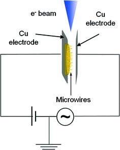
The precursors used to grow the nanowires were mixtures of Bi powder (Goodfellow, 99.997%) with either SnO2 (Sigma-Aldrich, 99.9%) or Er2O3 (Strem, 99.9%) powders. Mixtures containing Bi and 2, 5 10, 20 or 30 wt.% of SnO2 were compacted to form disk-shaped samples of about 7 mm diameter and 1 mm thickness. Five different mixtures containing 2, 5 10, 20 or 30 wt.% of Er2O3 were prepared following the same method. The samples were then annealed in a horizontal tube furnace, not sealed for vacuum conditions, under argon flow at 800 °C for times between 4 and 10 hours. Transport and oxidation of bismuth took place during the thermal treatments, leading to the growth of bismuth oxide nanostructures, nanowires and complex nanowire hierarchical arrangements on the tube's wall. The structures were detached from the tube and deposited on a silicon substrate for characterization. Their morphology and size were investigated with a FEI Inspect SEM. The structure of the wires was investigated by XRD with an X'Pert PRO MRD diffractometer using Cu Kα radiation and by HRTEM with a Jeol JEM 2010F and a Jeol JEM 3100F microscope. EBSD of single microwires was performed in a FEI Inspect SEM with a Bruker e-FlashHR+ system using an accelerating voltage of 20 kV. The composition of the samples was assessed by EDX in the SEM and TEM by using a Bruker QUANTAX and an Oxford INCA system, respectively. PL measurements were carried out at room temperature in a Horiba Jovin-Yvon LabRAM HR800 system. The samples were excited by a 325 nm He–Cd laser on an Olympus BX 41 confocal microscope. The study of mechanical resonances was carried out on Bi2O3 microwires with lengths ranging from 100 to 700 μm and cross-sectional dimensions of 0.5–3.5 μm. For the synthesis of these larger structures, no Er or Sn oxides were added to the precursor and the growth took place on the compacted Bi2O3 disk during annealing at 650 °C for 1.5 h under argon flow. In order to investigate the resonant behaviour of these samples, the disk with the microwires was glued with silver paste on a copper electrode and placed in front of a second copper electrode inside the chamber of a FEI Inspect SEM, as shown in Fig. 1. An oscillating voltage with an amplitude of 3–5 V and a frequency range of 0.1–100 kHz was applied with a Stanford Research SR830 DSP lock-in amplifier, while a 20 V constant voltage bias was simultaneously applied with a Keithley 2400 SourceMeter. The amplitude of the oscillating wire was measured, from the SEM images, as a function of the voltage frequency and the resonance frequency corresponding to the amplitude maximum was determined. The Young's modulus of the wire was then calculated from elasticity theory by using the experimental resonance frequencies.3. Results and discussion
3.1 Morphology, structure and composition
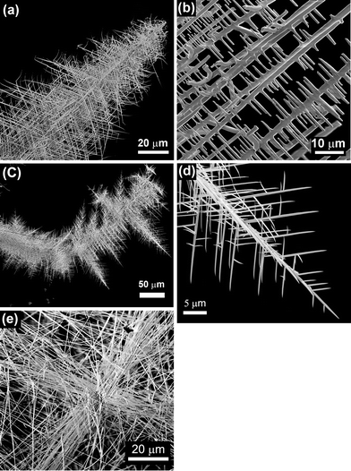
Hierarchical structures formed by a network of branched wires growing from a central axis are observed after the thermal treatment at 800 °C for 10 h of the SnO2 containing precursor, as shown in the low-magnification SEM image in Fig. 2a. These complex architectures were not obtained for shorter treatments. A higher magnification SEM image (Fig. 2b) shows secondary parallel rods with widths of about 1 to 3 μm and smaller perpendicular branches, most of them with cross-sectional dimensions of some hundreds of nanometers. Similar hierarchical structures, as well as wool-like arrangements of thinner wires (100–200 nm diameter), are formed when the Er-containing precursor is treated also at 800 °C for 10 h (Fig. 2c–e). Mixtures with oxide contents (either SnO2 or Er2O3) below 20 wt.% give rise to a lower amount of hierarchical structures, while no noticeable difference in terms of morphology or density of branched structures was observed when a mixture containing 30 wt.% of the corresponding oxide was used. In addition, when a mesh of pure Bi was used as the only precursor, just large microrods and microcrystals, without any hierarchical structures, were obtained.8 This shows that for Bi2O3, as in the case of ref. 21–27, the addition of an atomic fraction of certain cations to the precursor favours the hierarchical growth of oxide nanostructures. It is to be noticed that, contrary to the well-known catalyst-assisted vapour–liquid–solid (VLS) nanowire growth, no catalyst nanodrops at the tip of the wires were observed. In fact – as described below – according to the analytical techniques used in the present work, significant amounts of Er and Sn were not incorporated into the as-grown nanostructures. This is probably due to the big difference between our growth temperature (800 °C) and the melting and boiling temperatures of Er2O3 (2345 °C and 3290 °C, respectively) and SnO2 (1630 °C and 1800 °C, respectively). Although the obtained nanowires do not show a tapered morphology or Bi droplets at their tips, as confirmed by SEM, TEM and EDX measurements, autocatalytic processes cannot be in principle completely discarded. A small thin Bi layer, even atomically flat, might be present at the growth front, which could lead to growth via a VLS mechanism. The layer could be quickly oxidized during cooling or after exposure of the nanostructures to air after the growth, and a subsequent analysis may never find this layer.29 Nevertheless, in the particular case of Bi2O3, the formation of thin Bi layers or droplets has been reported to give rise to samples with micro- or nanoribbon morphology.19 In any case, as previously mentioned, hierarchical Bi2O3 arrangements were not obtained after thermal treatments of pure Bi, while a lower density of such arrangements was obtained when mixtures of Bi with low SnO2 or Er2O3 contents were used as precursors. These observations indicate that the addition of both metal oxides play a critical role in the growth of our branched, hierarchical nanostructures, probably increasing the number of nucleation sites, which is related to the surface energy of the crystal, temperature, and the supersaturated ratio of vapor.30 We believe that growth in the present case is governed by a vapour–solid (VS) process, in which the vapour originates from the precursor in a high-temperature zone and thereby facilitates the formation of the micro- and nanostructures in a low-temperature zone by the assistance of the Ar flow. The VS mechanism has been invoked in order to explain the formation of several hierarchical nanostructures in the presence of alloying elements.22–26 The fact that side branching is observed only in the presence of such elements strongly suggests that surface segregation may play an important role. During the growth of the central nanowire, the alloying content is continuously segregated to the boundaries of the nanowire core. The alloy-rich layer of the boundaries became the nucleation sites for the subsequent growth of side branches.22 As stated before, this mechanism has been proposed to explain the formation of ZnO hierarchical nanostructures when small amounts of In2O3,22 SnO2,23,24 Eu2O3 (ref. 25) or Al2O3 (ref. 26) were added to the precursor material. In the present case, no segregation was detected by SEM or TEM-EDX spectroscopy in the main trunk or in the branches of the structures, but incorporation of a small concentration of metallic elements (Sn and Er) below the EDX detection limit is certainly possible. In fact, previous studies reported alloying metallic element contents below 0.5 at% in certain areas of the hierarchical nanostructures, while in others such elements were not detected.25,26The XRD spectra of all the grown samples were indexed to the monoclinic α-Bi2O3 phase (JCPDS card 041-1449), regardless of the precursor used and the final morphology of the structures (Fig. 3). Moreover, no diffraction maxima related to pure Sn, Er or their corresponding oxides were observed. EDX spectra in SEM (Fig. 4) or TEM reveal only peaks corresponding to Bi and O and no Sn or Er signals were detected. For these reasons, the structures obtained from both kinds of precursors were considered to be equivalent regarding crystallography and composition. Since the presence of Er2O3 yielded thin nanowires and a higher density of branched structures, mainly the samples obtained from the precursor mixture Bi–Er2O3 were further investigated.
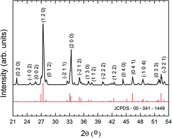 | ||
| Fig. 3 XRD pattern representative of the hierarchical structures. All the diffraction maxima can be indexed to the monoclinic α-Bi2O3 phase (JCPDS card 041-1449). | ||
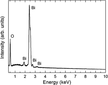 | ||
| Fig. 4 SEM-EDX spectrum of Bi2O3 nanowires grown from the precursor containing Er2O3. Only peaks related to O and Bi can be appreciated. | ||
Individual nanowires with diameters of several hundreds of nanometres were selected for EBSD characterization in the SEM. EBSD allows crystallographic information to be obtained from samples in the SEM by striking an electron beam on a tilted sample and obtaining the diffracted electron pattern with the aid of a fluorescent phosphor screen. The variations in the intensity of the diffracted electrons as a function of direction form patterns of Kikuchi lines. These diffraction patterns are then analyzed by computer software and used to measure the wire crystal orientation, discriminate between different materials and provide information about extended defects. EBSD was found to be particularly useful for the structural characterization of our Bi2O3 thicker structures, which cannot be properly investigated by TEM. Such structures usually show smooth, well-faceted faces, where EBSD measurements can be carried out. A representative example of the acquired patterns is displayed in Fig. 5. The diffraction patterns did not change when the electron beam was moved along the length of the wire. The obtained results reveal that all the wires investigated are of monoclinic structure and belong to the α-Bi2O3 phase, usually with a [011] zone axis. Our EBSD studies did not reveal the presence of extended defects in these samples.
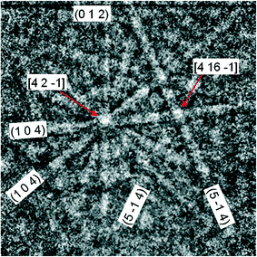 | ||
| Fig. 5 Indexed EBSD pattern of a 500 nm wide Bi2O3 wire with the symmetries of the monoclinic α phase. | ||
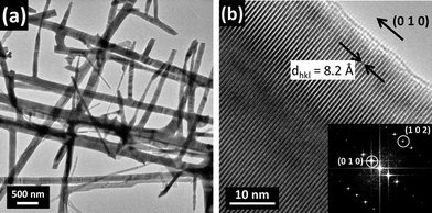
Low-magnification TEM images of the secondary nanowires (those that stem from the central axis) show branched nanostructures with lengths up to 15 μm and diameters in the 40–300 nm range (Fig. 6a). A high-resolution micrograph of a 100 nm wide nanowire and the corresponding FFT pattern are shown in Fig. 6b. Indexing of the FFT pattern and analysis of this and other images confirm that the wires belong to the monoclinic α-phase, as it was already reported for Bi2O3 nanowires grown by a similar procedure.31 The mentioned image shows fringes running perpendicular to the edge of the nanowire. The fringe spacing measures 0.82 nm, which corresponds to the (010) interplanar spacing. This shows the single crystalline nature of the wire that grows along the [010] direction. A TEM image of the junction between two perpendicular nanowires is shown in Fig. 7a. HRTEM images of these regions, as that shown in Fig. 7b, revealed that the branched Bi2O3 nanowires have single-crystal structures with clean backbone-to-branch junctions. No extended defects were found in our HRTEM observations of similar areas, which strongly suggest that growth mechanisms driven by screw dislocations32 or twins33 may be ruled out.
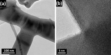 | ||
| Fig. 7 (a) TEM micrograph of the junction between two perpendicular nanowires. (b) HRTEM image of the same area showing single-crystal structures with no extended defects. | ||
3.2 Luminescence
The influence of the precursor on the luminescence of the nanowires has been investigated by PL excited by 325 nm laser light. Although no Sn or Er has been detected in the analysis of the nanowires, the luminescence can provide information on the possible indirect effects of the addition of their oxides on the final defect structure and, in the case of Er, on the presence of traces of optically active ions. In fact, the addition of Al2O3 to a ZnS precursor used to grow ZnO structures with the same vapour–solid method used in this work has been found to induce the formation of branched nanorod networks and cathodoluminescence (CL) spectral changes without apparent Al incorporation into the structures, as measured by EDX.26 These studies demonstrated that nanorod networks fabricated with an Al2O3-containing precursor show an emission band, attributed to oxygen excess, which is not observed in materials prepared without Al2O3 or other oxides. In the present work, we compare the PL of the nanowires with previously reported PL studies of Bi2O3 sintered ceramics34 and nanostructures.13,35Fig. 8 shows the PL spectra of the nanowires grown with SnO2 or Er2O3 in the precursor and a representative spectrum of Bi2O3 ceramics prepared by sintering pure Bi2O3 powders at 500 °C for 10 h. The obtained results indicate that modifying the composition of the source materials changes not only the morphology of the grown oxide nanostructures, but also their luminescence properties. Actually, it can be observed that the three spectra have their maxima at different energies. The observed shifts cannot be attributed to quantum confinement effects or residual stresses within the Bi2O3 nanowires,13 since SEM images reveal nanostructures with dimensions above 100 nm, while TEM observations provide no evidence of lattice distortions. As explained below, the different peak positions observed in the PL spectra of nanowires grown by adding the mentioned two oxides are due to the relative weights of the different emission bands contributing to the overall spectrum in each case.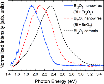 | ||
| Fig. 8 PL spectra of α-Bi2O3 nanowires grown from different precursors and of a bulk ceramic sample sintered for comparison purposes. | ||
The spectrum of the ceramic sample is peaked at 2.33 eV (532 nm), but previous CL investigations reveal the existence of other components at about 1.91 eV and 2.83 eV.34 The 2.33 eV and the 1.95 eV emission bands have been attributed to a Bi ion in the closest environment of three oxygen ions.36 Actually, trivalent bismuth cations in inorganic compounds exhibit interesting luminescence properties related to their 6s2 configuration.37,38 Above 80 K, radiative transitions are mainly assigned to 3P1 → 1S0 transitions13,35,37 or charge transfer transitions between oxygen ligands and Bi3+ ions,38 giving rise to luminescence spectra peaked in the blue to green region under UV excitation. On the other hand, Bi2+ ions show PL emission in the range 2.10–1.95 eV under UV excitation. This luminescence has been attributed to 2P3/2(1) → 2P1/2 transitions35,39,40 and it is extremely dependent on the local crystal field, which in turn depends on the symmetry and coordination of the surrounding oxygen atoms. Our luminescence studies of Bi2O3 bulk samples annealed in different atmospheres have shown that a 2.1 eV band is related to oxygen vacancies.34Fig. 8 shows that the PL bands of the nanowires synthesized with precursors containing SnO2 and Er2O3 appear peaked at 2.12 eV (585 nm) and 1.92 eV (646 nm), respectively. This indicates that the presence of Sn in the precursor favours the growth of nanowires with a higher concentration of oxygen vacancies. The diffusion of Bi ions has been previously considered to predominate over the diffusion of oxygen ions during the growth of complex Bi2O3 architectures by thermal oxidation of Bi, which resulted in the formation of a high density of oxygen vacancies.41 In the case of the samples grown from the Er-containing precursor, the site symmetry and oxygen coordination around the reduced Bi ions favour an intense PL signal related to Bi2+ intraionic transitions.
3.3 Young's modulus
The characterization of the mechanical properties of semiconductor nanowires and other elongated nanostructures is a subject of interest related to their applications in NEMS, micromechanical sensors and optomechanical coupling devices.42 The Young's modulus of elongated nanostructures of different materials has been determined by electric field-induced mechanical resonance, nanoindentation and atomic force microscopy. For reviews on mechanical characterization of nanowires, see ref. 42 and 43. In situ TEM measurements of mechanical resonance under an applied electric field has enabled the determination of the Young's modulus of ZnO nanobelts,44 BN nanotubes,45 carbon nanotubes,46 or GaN nanowires.47 Similar in situ SEM studies, which would enable one to investigate larger nanowires, have been only occasionally reported.48 Measurements by mechanical resonance techniques and AFM have shown, in some cases, a strong dependence of the Young's modulus of elongated nanostructures on geometrical parameters, such as the diameter of nanotubes43 and nanowires48 or the width-to-thickness ratio of nanobelts.49 In order to study such potential effects in our nanowires, the Young's modulus has been determined for a total of fourteen wires with different lengths and cross-sectional dimensions. By applying an alternating potential at the electrodes in the arrangement shown in the schematic in Fig. 1, the nanowires are deflected by the electrostatic force, leading to oscillations with the potential frequency. By measuring in the SEM screen the oscillation amplitude as a function of the frequency, an amplitude peak appears at the resonance frequency of the nanowire. In the present case, the resulting first harmonic resonance frequencies vary from 2 to 17 kHz. From elasticity theory,50 this resonance frequency is | (1) |
 | (2) |
| E = (νL2/0.28r)2ρ | (3) |
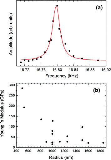
Fig. 9a and b, respectively, show SEM images of a 250 μm long wire of 1 μm radius at rest and vibrating under the applied electric field. The amplitude–frequency curve of a wire of 500 nm radius is shown in Fig. 10a. The resonance frequency measurements of fourteen wires of different radii and lengths yielded a noticeable dispersion of E values, which ranged from 11 to 284 GPa. The relationship of the Young's modulus to the radius of the wires has been plotted in Fig. 10b. A general trend of a lower Young's modulus for a higher radius can be appreciated. Such a trend is qualitatively similar to that reported for ZnO,48 CuO,51 WO3,52,53 Ag and Pb nanowires,54 but in the present case the effect is observed for larger radii. In some studies, the measured values of E approach the bulk value as the radius of the nanowire increases.47,48,51 This size dependence has been explained for ZnO nanowires in terms of surface stiffening arising from the gradually shortened bond lengths from the nanostructure central region to the surface.48 A similar trend has also been reported for CuO nanowires and attributed to the formation of an amorphous layer in the smaller nanostructures.51 However, in other cases the opposite trend has been observed, i.e., the Young's modulus approaches the bulk value as the radii of the nanowires decrease.52,53 This has been explained by differences in the defect structure of nanowires with different diameters. Since we are not aware of previous studies reporting the Young's modulus of α-Bi2O3, a bulk ceramic sample of this oxide was prepared by sintering pure Bi2O3 powder at 750 °C for 10 h. The ceramic was mirror-polished and the corresponding Young's modulus was determined by nanoindentation.55 The obtained value, 105 ± 4 GPa, is included in the interval shown in Fig. 10a and is also in good agreement with the 104 GPa value that can be deduced from the elastic constants calculated by Music et al.56 for bulk δ-Bi2O3. These results suggest that surface effects do not play a dominant role in the observed trend of E as a function of the wire radius.
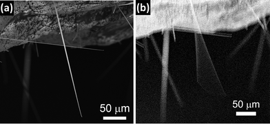 | ||
| Fig. 9 SEM images of an α-Bi2O3 nanowire at rest (a) and vibrating under an applied alternating electric field (b). | ||
The quality factor Q of the microwires as mechanical resonators can be estimated from fitting of the resonance curves to Lorentzian profiles, as expected for damped harmonic vibrations, according to the relationship Q = νr/Δν, where νr is the peak resonance frequency and Δν is the full width at half maximum of the resonance peak. The inverse factor 1/Q is related to energy dissipation. Since the wires vibrate at SEM vacuum (~10−6 Torr), the energy dissipation arising from air damping can be neglected; it mainly originates from the intrinsic properties of the material. Measurements of Q in the obtained resonance curves yield values in the range 650–750. Reported quality factors for mechanical resonances of semiconducting nanowires or nanotubes extend over a wide range of values, which are in many cases comparable to those measured in this work, e.g., 120 for V2O5 nanowires,57 20–750 for SiO2 nanowires,58 340 for boron nitride nanotubes,45 500 for ZnO nanobelts44 or 80–700 for MoS2 diaphragms.59 These results show that Bi2O3 wires may have potential application as micromechanical resonators.
4. Conclusions
Hierarchical Bi2O3 nano- and microwires grown by a thermal evaporation–deposition method have been investigated. The addition of SnO2 or Er2O3 to the main Bi precursor favours the formation of hierarchical, multibranched arrangements. The incorporation of Er or Sn into Bi2O3 nanostructures was not detected by SEM or TEM-EDX microanalysis, but both metallic elements may be present in concentrations below the detection limit of this analytical technique. XRD, EBSD and HRTEM measurements reveal the good crystallinity of the grown samples, the structure of which corresponds to the monoclinic α-Bi2O3 phase. The composition of the precursors influences not only the morphology but also the luminescence properties of the oxide nanostructures. The PL of the nanowires shows that the relative intensities of the emission bands associated with Bi2+ ions and oxygen vacancies depend on the composition of the precursor used to grow the nanostructures. In situ SEM mechanical resonance induced by an alternating electric field has been used to determine the Young's modulus of the microwires. A noticeable dispersion of E values has been obtained with a trend toward smaller values for increasing radius of the microwires. The quality factors measured for the microstructures suggest that Bi2O3 wires may have potential application as micromechanical resonators.Acknowledgements
This work has been supported by MINECO through projects CSD2009-00013, MAT 2012-31959 and MAT 2010-16407.References
- Y. Cui and C. M. Lieber, Science, 2001, 291, 851–853 CrossRef CAS PubMed
.
- M. Willander, L. L. Yang, A. Wadeasa, S. U. Ali, M. H. Asif, Q. X. Zhao and O. Nura, J. Mater. Chem., 2009, 19, 1006–1018 RSC
.
- G. Wang, H. Tanaka, L. Hong, Y. Matsuo, K. Niikura, M. Abe, K. Matsumoto, T. Ogawab and K. Ijiro, J. Mater. Chem., 2012, 22, 13691–13697 RSC
.
- Z. L. Wang, J. Phys.: Condens. Matter, 2004, 16, R829–R858 CrossRef CAS
.
- C. Li, D. Zhang, X. Liu, S. Han, T. Tang, J. Han and C. Zhou, Appl. Phys. Lett., 2003, 82, 1613–1615 CrossRef CAS PubMed
.
- L. Cheng, M.-W. Shao, D. Chen, D. D. D. Ma and S.-T. Lee, CrystEngComm, 2010, 12, 1536–1539 RSC
.
- H. Gobrecht, S. Seeck, H. E. Bergt, A. Märtens and K. Kossmann, Phys. Status Solidi, 1969, 33, 599–606 CrossRef CAS
.
- M. Vila, C. Díaz-Guerra and J. Piqueras, J. Alloys Compd., 2013, 548, 188–193 CrossRef CAS PubMed
.
- A. Cabot, A. Marsal, J. Arbiol and J. R. Morante, Sens. Actuators, B, 2004, 99, 74–89 CrossRef CAS PubMed
.
- A. Hameed, T. Montini, V. Gombac and P. Fornasiero, J. Am. Chem. Soc., 2008, 130, 9658–9659 CrossRef CAS PubMed
.
- L. Leontie, M. Caraman, M. Alexe and C. Harnagea, Surf. Sci., 2002, 480, 507–510 Search PubMed
.
- M. Vila, C. Díaz-Guerra and J. Piqueras, J. Mater. Chem. C, 2013, 1, 7920–7929 RSC
.
- L. Kumari, J.-H. Lin and Y.-R. Ma, J. Phys.: Condens. Matter, 2007, 19, 406204 CrossRef PubMed
.
- Y. Qiu, M. Yang, H. Fan, Y. Zuo, Y. Shao, Y. Xu, X. Yanga and S. Yang, CrystEngComm, 2011, 13, 1843–1850 RSC
.
- H. W. Kim, J. W. Lee and C. Lee, J. Korean Phys. Soc., 2007, 50, 1308–1311 CrossRef CAS
.
- X. P. Shen, S. K. Wu, H. Zhao and Q. Liu, Phys. E, 2007, 39, 133–136 CrossRef CAS PubMed
.
- S. Park, H. Kim, C. Lee, D. H. Lee and S. S. Hong, J. Korean Phys. Soc., 2008, 53, 1965–1970 CAS
.
- X. Gou, R. Li, G. Wang, Z. Chen and D. Wexler, Nanotechnology, 2009, 20, 495501 CrossRef PubMed
.
- B. Ling, X. W. Sun, J. L. Zhao, Y. Q. Shen, Z. L. Dong, L. D. Sun, S. F. Li and S. Zhang, J. Nanosci. Nanotechnol., 2010, 10, 8322–8327 CrossRef CAS PubMed
.
- D. Chen, Z. Liu, X. Wang, B. Liang, J. Xu, H. Huang, Z. Xiea and G. Shen, CrystEngComm, 2011, 13, 7305–7310 RSC
.
- J. Yu Lao, J. G. Wen and Z. F. Ren, Nano Lett., 2002, 2, 1287–1291 CrossRef CAS
.
- J. G. Wen, J. Y. Lao, D. Z. Wang, T. M. Kyaw, Y. L. Foo and Z. F. Ren, Chem. Phys. Lett., 2003, 372, 717–722 CrossRef CAS
.
- P. Gao and Z. L. Wang, J. Phys. Chem. B, 2002, 106, 12653–12658 CrossRef CAS
.
- Y. Ortega, P. Fernández and J. Piqueras, J. Cryst. Growth, 2009, 311, 3231–3234 CrossRef CAS PubMed
.
- Y. Ortega, P. Fernández and J. Piqueras, J. Nanosci. Nanotechnol., 2010, 10, 502–507 CrossRef CAS PubMed
.
- Y. Ortega, P. Fernández and J. Piqueras, Semicond. Sci. Technol., 2011, 26, 085035 CrossRef
.
- P. Hidalgo, B. Méndez and J. Piqueras, Nanotechnology, 2008, 19, 455705 CrossRef CAS PubMed
.
- I. López, E. Nogales, B. Méndez, J. Piqueras, A. Peche, J. Ramírez-Castellanos and J. M. González-Calbet, J. Phys. Chem. C, 2013, 117, 3036–3045 Search PubMed
.
- Z. R. Zai, Z. W. Pan and Z. L. Wang, Adv. Funct. Mater., 2003, 13, 9–24 CrossRef
.
- S. L. Mensah, A. Prasad, J. Wang and Y. K. Yap, J. Nanosci. Nanotechnol., 2008, 8, 233–236 CrossRef CAS PubMed
.
- M. Vila, C. Díaz-Guerra and J. Piqueras, Appl. Phys. Lett., 2012, 101, 071905 CrossRef PubMed
.
- J. Zhu, H. Peng, A. F. Marshall, D. M. Barnett, W. D. Nix and Y. Cui, Nat. Nanotechnol., 2008, 3, 477–481 CrossRef CAS PubMed
.
- D. Li, F. Soberanis, J. Fu, W. Hou, J. Wu and D. Kisailus, Cryst. Growth Des., 2013, 13, 422–428 CAS
.
- M. Vila, C. Díaz-Guerra and J. Piqueras, Mater. Chem. Phys., 2012, 133, 559–564 CrossRef PubMed
.
- L. Kumari, J.-H. Lin and Y.-R. Ma, Nanotechnology, 2007, 18, 295605 CrossRef
.
- O. M. Bordun, I. I. Kukhasrskii, V. V. Dmitruk, V. G. Antonyuk and V. P. Savchin, J. Appl. Spectrosc., 2008, 75, 681–684 CrossRef CAS
.
- G. Blasse, H. Zhiran, A. J. A. Winnubst and A. J. Burggraaf, Mater. Res. Bull., 1984, 19, 1057–1062 CrossRef CAS
.
- Y. Zorenko, V. Gorbenko, T. Voznyak, V. Jary and M. Nikl, J. Lumin., 2010, 130, 1963–1969 CrossRef CAS PubMed
.
- A. M. Srivastava, J. Lumin., 1998, 78, 239–243 CrossRef CAS
.
- M. Gaft, R. Reisfeld, G. Panczer, G. Boulon, T. Saraidarov and S. Erlish, Opt. Mater., 2001, 16, 279–290 CrossRef CAS
.
- X. Liu, W. Bian and C. Tian, Mater. Lett., 2013, 112, 1–4 CrossRef CAS PubMed
.
- C. Röhling, M. Niebelschütz, K. Brueckner, K. Tonisch, O. Ambacher and V. Cimalla, Phys. Status Solidi B, 2010, 247, 2557–2570 CrossRef
.
-
Z. L. Wang, Dekker Encyclopedia of Nanoscience and Nanotechnology, ed. J. A. Schwarz, C. Contescu and K. Putyera, Marcel Dekker, Inc., 2004, pp. 1773–1786 Search PubMed
.
- X. D. Bai, P. X. Gao, Z. L. Wang and E. G. Wang, Appl. Phys. Lett., 2003, 82, 4806–4808 CrossRef CAS PubMed
.
- A. P. Suryavanshi, M. Yu, J. Wen, C. Tang and Y. Bando, Appl. Phys. Lett., 2004, 84, 2527–2529 CrossRef CAS PubMed
.
- P. Poncharal, Z. L. Wang, D. Ugarte and W. A. de Heer, Science, 1999, 283, 1513–1516 CrossRef CAS
.
- C.-Y. Nam, P. Jaroenapibal, D. Tham, D. E. Luzzi, S. Evoy and J. E. Fischer, Nano Lett., 2006, 6, 153–158 CrossRef CAS PubMed
.
- C. Q. Chen, Y. Shi, Y. S. Zhang, J. Zhu and Y. J. Yan, Phys. Rev. Lett., 2006, 96, 075505 CrossRef CAS
.
- M. Lucas, W. Mai, R. Yang, Z. L. Wang and E. Riedo, Nano Lett., 2007, 7, 1314–1317 CrossRef CAS PubMed
.
-
W. Weaver, S. P. Timoshenko and D. H. Young, Vibration Problems in Engineering, John Wiley & Sons Inc., New York, 5th edn, 1990 Search PubMed
.
- E. P. S. Tan, Y. Zhu, T. Yu, L. Dai, C. H. Sow, V. B. C. Tan and C. T. Lin, Appl. Phys. Lett., 2007, 90, 163112 CrossRef PubMed
.
- K. H. Liu, W. L. Wang, Z. Xu, L. Liao, X. D. Bai and E. G. Wang, Appl. Phys. Lett., 2006, 89, 221908 CrossRef PubMed
.
- F. C. Cheong, B. Varghese, Y. Zhu, E. P. S. Tan, L. Dai, V. B. C. Tan, C. T. Lim and C. H. Sow, J. Phys. Chem. C, 2007, 111, 17193–17199 Search PubMed
.
- S. Cuenot, C. Frétigny, S. Demoustier-Champagne and B. Nysten, Phys. Rev. B: Condens. Matter Mater. Phys., 2004, 69, 165410 CrossRef
.
- J. Molina, private communication, E-mail: jon.molina@imdea.org.
- D. Music, S. Konstantinidis and J. M. Schneider, J. Phys.: Condens. Matter, 2009, 21, 175403 CrossRef PubMed
.
- Y. Zhu, Y. Zhang, L. Dai, F.-C. Cheong, V. Tan, C.-H. Sow and C.-T. Lim, Acta Mater., 2010, 58, 415–420 CrossRef CAS PubMed
.
- D. A. Dikin, X. Chen, W. Ding, G. Wagner and R. S. Ruoff, J. Appl. Phys., 2003, 93, 226–230 CrossRef CAS PubMed
.
- J. Lee, Z. Wang, K. He, J. Shan and P. X.-L. Feng, ACS Nano, 2013, 7, 6086–6091 CrossRef CAS PubMed
.
| This journal is © The Royal Society of Chemistry 2015 |

