Extraordinary role of Hg in enhancing the thermoelectric performance of p-type SnTe†
Gangjian
Tan‡
a,
Fengyuan
Shi‡
b,
Jeff W.
Doak‡
b,
Hui
Sun‡
c,
Li-Dong
Zhao‡
a,
Pengli
Wang‡
a,
Ctirad
Uher‡
c,
Chris
Wolverton‡
b,
Vinayak P.
Dravid‡
b and
Mercouri G.
Kanatzidis‡
*ad
aDepartment of Chemistry, Northwestern University, Evanston, Illinois 60208, USA. E-mail: m-kanatzidis@northwestern.edu
bDepartment of Materials Science and Engineering, Northwestern University, Evanston, Illinois 60208, USA
cDepartment of Physics, University of Michigan, Ann Arbor, Michigan 48109, USA
dMaterials Science Division, Argonne National Laboratory, Argonne, Illinois 60439, USA
First published on 23rd October 2014
Abstract
We report several synergistic effects in Hg alloying of SnTe to enhance the power factor and overall figure of merit ZT. Hg alloying decreases the energy separation between the two valence bands, leading to pronounced band convergence that improves the Seebeck coefficient. Hg alloying of SnTe also significantly enlarges the band gap thereby effectively suppressing the bipolar diffusion. Collectively, this results in high ZT of ∼1.35 at 910 K for 2% Bi-doped SnTe with 3%HgTe. The solubility limit of Hg in SnTe is less than 3 mol%, and above this level we observe HgTe precipitates in the SnTe matrix, typically trapped at grain boundary triple junctions. The strong point defect scattering of phonons caused by Hg alloying coupled with mesoscale scattering via grain boundaries contributes to a great reduction of lattice thermal conductivity. The multiple synergistic roles that Hg plays in regulating the electron and phonon transport in SnTe provide important new insights into continued optimization of SnTe-based and related materials.
Broader contextBand engineering is an efficient way of enhancing the thermoelectric performance of typical semiconductors. It usually incorporates resonant levels, band degeneracy, and band gap tuning through chemical doping approaches. Herein we show that a tiny amount of HgTe alloying could not only significantly diminish the energy separation between the two valence bands in SnTe, leading to enhanced Seebeck coefficient, but notably enlarge the band gap of SnTe, giving rise to suppressed bipolar diffusion. The considerable point defect scattering by Hg alloying in combination with excess HgTe forming mesoscale structures results in great reduction in the lattice thermal conductivity. The synergistic role that Hg plays in SnTe leads to a record high ZT of 1.35 at 910 K. |
1. Introduction
Thermoelectric materials, capable of realizing the direct conversion between heat and electricity, have received worldwide attention due to their potential in playing a role in energy efficiency.1–6 Materials systems that can operate around 500–900 K are particularly attractive because most of the waste heat in industry and automobile exhaust is within this range.7–9 To date, the leading materials are lead chalcogenides,10–17 filled skutterudites,18–22 and some diamond-like compounds.23–25 Several advances in this field have been achieved in PbTe-based materials with the highest figure of merit ZT exceeding 2 at 915 K. This was accomplished by synergistically applying the concepts of band structure engineering and microstructure modification (panoscopic approach).12,26 Although lead chalcogenides have been extensively studied, their Sn-based analogues especially SnTe which is similar to PbTe in regards to crystal structure, crystal chemistry and general doping principles did not receive significant attention.27–30The main drawbacks of SnTe are the smaller band gap (0.18 eV at 300 K) and much larger energy separation (0.35 eV at 300 K) between the light-hole band at L point and heavy-hole band at Σ point with respect to PbTe (0.30 eV and 0.17 eV at 300 K, respectively).26,27,31,32 These result in significant bipolar conduction and lower Seebeck coefficient for SnTe when compared to PbTe at a similar carrier density level, and consequently SnTe exhibits considerably inferior thermoelectric performance. Attempts at modifying the valence band structure of SnTe have been made to improve its ZT value. Zhang et al.27 reported a resonant level near the Fermi level of SnTe introduced by indium doping and found a prominent enhancement of the Seebeck coefficient. In conjunction with a successful reduction of thermal conductivity through refined microstructure by ball milling, they reported a ZT of ∼1.1 around 873 K. Recently, we reported that Cd as an alloying element favorably impacts the band structure of SnTe in two aspects: (a) band gap enlargement and (b) valence band convergence, leading to suppressed bipolar diffusion and increased Seebeck coefficient. Concurrently, utilizing CdS/ZnS nanoscale precipitates as strong phonon scattering features, the lattice thermal conductivity of SnTe is considerably decreased. As a consequence, a maximum ZT of ∼1.3 at ∼873 K was achieved.33 These findings make SnTe-based materials a robust candidate for thermoelectric power generation application and warrant further investigation and optimization.
In this study, we explored another group 14 element, Hg, as a possible alloying addition for SnTe, with Bi as the electron donor dopant. Compared to Cd, Hg has additional advantages. Our experimental results and theoretical calculations unambiguously reveal that Hg is more efficient in producing valence band degeneracy than Cd. Moreover, the Sn1−xHgxTe samples exhibit lower lattice thermal conductivities than Cd-containing samples with comparable Hg and Cd concentration levels. When the Hg content exceeds its solubility of ∼2–3 mol%, large and isolated HgTe particles were found preferentially at grain boundaries and triple junctions, which are unlikely to contribute to any notable or effective phonon scattering. Therefore, we suggest that the point defects in the matrix created by Hg alloying are the primary reason for the lower lattice thermal conductivity in the HgTe containing samples, with expected smaller contribution from mesoscale grain boundaries. As a result, a high ZT of ∼1.35 at ∼910 K was obtained for the sample with nominal composition Sn0.98Bi0.02Te–3%HgTe, which is comparable to that of Cd-alloyed SnTe nanostructured with CdS. However, a much higher average ZT (ZTave) exceeding unity between 500 and 900 K is found in the Hg-alloyed samples, making them superior to the Cd-containing system.
2. Experimental procedures
Synthesis
Reagent chemicals were used as obtained: Sn chunk (99.9999%, American Elements, US), Bi shot (99.999%, American Elements, US), Cd shot (99.99%, Alfa, US), Hg liquid (99.99%, Baker, US), and Te shot (99.999%, 5 N Plus, Canada).Samples with nominal compositions Sn0.98Bi0.02Te–x%HgTe (x = 0, 0.5, 1, 2, 3, and 4, in mole fraction) and two control samples Sn0.98Bi0.02Te–x%CdTe (x = 2 and 3, in mole fraction) were prepared as follows. Appropriate amounts of Sn, Bi, HgTe, Cd, and Te were weighed and mixed in 10 mm diameter silica tubes. The tubes were then evacuated to a residual pressure of ∼10−4 Torr, flame-sealed, slowly heated to 1273 K, soaked at this temperature for 8 h, and quickly cooled to room temperature by water quenching. The resultant ingots were resealed in 13 mm diameter silica tubes and vacuum annealed at 673 K for 12 h, and then slowly cooled to room temperature by switching off the furnace power. For a typical experiment: Sn (3.6540 g, 30.7862 mmol), Bi (0.1313 g, 0.6283 mmol), HgTe (0.2062 g, 0.6283 mmol), and Te (4.0085 g, 31.4145 mmol) were used to prepare 8 g of Sn0.98Bi0.02Te–2%HgTe.
The melt grown ingots were ground into fine powders using a mechanical mortar and pestle to reduce the grains to less than 4 μm in diameter. These powders were then densified by spark plasma sintering (SPS) method (SPS-211LX, Fuji Electronic Industrial Co., Ltd.) at 773 K for 5 min in a 12.7 mm diameter graphite die under an axial pressure of 40 MPa in vacuum. Highly dense (>97% of theoretical density, Table S1†) disk-shaped pellets with dimensions of 12.7 mm diameter and 8 mm thickness were obtained.
Physical characterization
Electron microscopy and X-ray diffraction
Scanning and scanning transmission electron microscopy (STEM) investigations were carried out in a JEOL 2100F microscope operated at 200 kV. STEM energy dispersion spectroscopy (EDS) spectrum imaging (SI) was carried out with a Hitachi HD-2300 dedicated STEM equipped with high collection angle dual EDS detectors. Thin TEM specimens were prepared by conventional methods, including cutting, grinding, dimpling, tripod, with minimal duration of Ar-ion milling, and followed by liquid nitrogen cooled, low energy (900 eV) ion milling by Fischione Nanomill. Samples pulverized with an agate mortar were used for powder X-ray diffraction (XRD). The powder diffraction patterns were obtained with Cu Kα (λ = 1.5418 Å) radiation in a reflection geometry on an INEL diffractometer operating at 40 kV and 20 mA and equipped with a position-sensitive detector.Band structure calculations
Density functional theory (DFT)34,35 calculations of the band structures of SnTe, Cd-doped SnTe, and Hg-doped SnTe were carried out using the Vienna Ab initio Simulation Package (VASP).36–39 Calculations were performed with projector-augmented wave (PAW)40 potentials and the exchange-correlation functional of Perdew, Burke, and Erzenhoff (PBE)41 using spin–orbit coupling (SOC). Potentials for Sn, Cd, Hg, and Te, contained the 4d105s25p2, 4d105s2, 5d106s2, and 5s25p4 electrons as valence, respectively.42 Cd- and Hg-doped SnTe calculations were performed on 54-atom supercells created by replacing 1 Sn atom with either Cd or Hg in a 3 × 3 × 3 supercell of the rocksalt primitive cell of SnTe. There is no ambiguity in the choice of the Sn site for Hg or Cd substitution because all 27 Sn atoms in the 54-atom supercell are symmetrically equivalent. The pure SnTe supercell and doped supercells were relaxed using the relaxation scheme of the Open Quantum Materials Database (OQMD),43 with a subsequent relaxation with 520 eV plane-wave basis cutoff energies, 5 × 5 × 5 Γ-centered k-point meshes, and tetrahedral k-point integration. Band structure calculations were performed for each of the supercells using 520 eV cutoff energies and 20 k-points along each of the lines from L to Γ and from Γ to K in the 54-atom rocksalt supercell Brillouin Zone.The electron eigenvalues of the Cd- and Hg-doped SnTe band structures were aligned to the electron eigenvalues of the pure SnTe band structure through an alignment procedure making use of the electrostatic potentials of the pure and doped supercells.44 The electrostatic potential was averaged around each atom in the pure, Cd-, and Hg-doped supercells. The difference between these atom-averaged electrostatic potentials in the doped and pure supercells were taken and averaged over each atom lying outside a sphere with a radius of one half the defect (Cd or Hg) periodic image distance, centered at the defect. Subtracting this cell-averaged electrostatic potential difference from the electron eigenvalues of the defect supercells aligns the band structure of the defected supercells with the band structure of the pure SnTe supercell, placing the band structures on the same energy scale and allowing for accurate comparisons between the band structures of pure, Cd-, and Hg-doped SnTe.
3. Results and discussion
Solubility limit of HgTe in 2 mol% Bi-doped SnTe
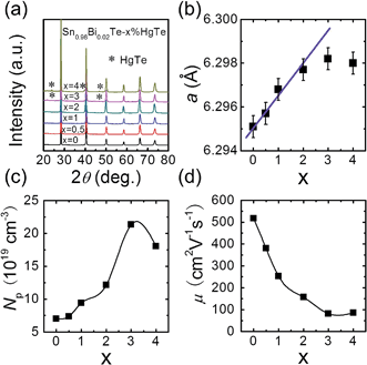
The PXRD patterns for samples of Sn0.98Bi0.02Te–x%HgTe show NaCl-type structure as the main phase for all samples and for x ≥ 3 a trace amount of cubic HgTe as a second phase, Fig. 1(a). Similarly, we find that one of the control samples (alloying with Cd) Sn0.98Bi0.02Te–2%CdTe shows single phase while at 3% CdTe we observe a trace of CdTe as a second phase, see ESI (Fig. S3†). As can be seen from Fig. 1(b), the lattice parameter increases with increasing x until x = 2 and beyond that it saturates. The increase in SnTe lattice parameter upon HgTe alloying is consistent with the fact Hg2+ (ionic radius 0.110 nm) is larger than Sn2+ (0.093 nm). The measured room temperature hole density is plotted in Fig. 1(c), which shows an increasing trend with increasing x, although Hg is supposed to be isovalent with Sn. The hole mobility, however, decreases with increasing x, Fig. 1(d), probably due to alloy scattering, and higher effective mass of holes caused by band structure modification, which we will discuss later. Collectively, both the lattice parameter and hole density variations suggest that the solubility limit of HgTe in Sn0.98Bi0.02Te is between 2% and 3%, which is higher than the ∼1.5 mol% observed by Nasirov et al.45Electrical transport properties
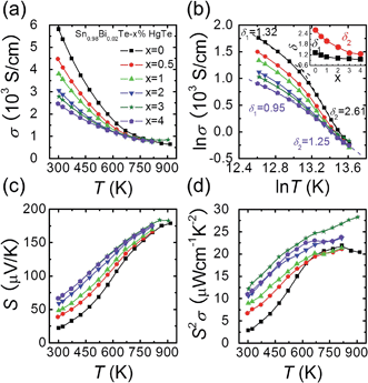
Fig. 2(a) shows the electrical conductivity as a function of temperature for Sn0.98Bi0.02Te–x%HgTe. Clearly, the room temperature electrical conductivity decreases significantly from ∼5815 S cm−1 in Sn0.98Bi0.02Te to ∼2467 S cm−1 for the sample with 4%HgTe. This reduction in electrical conductivity is mainly attributed to the decrease in carrier mobility, Fig. 1(d). Similar to the case of PbTe and PbSe,46,47 modeling the electrical conductivity of SnTe-based materials with a single power law dependence of the form σ ∼ T−δ is inadequate. Instead, two distinct regions with two different δ (δ1 in the low temperature range and δ2 in the high temperature range) values can be extracted from the ln![[thin space (1/6-em)]](https://www.rsc.org/images/entities/char_2009.gif) σ–ln
σ–ln![[thin space (1/6-em)]](https://www.rsc.org/images/entities/char_2009.gif) T plot, Fig. 2(b). The inset of Fig. 2(b) shows plots δ1 and δ2 as a function of x, both of which decrease evidently with increasing HgTe content. The much smaller δ values in the HgTe-containing samples imply a much weaker temperature dependence of hole scattering at high temperature. Therefore, at high temperature, these samples have comparable or even higher electrical conductivities than the Sn0.98Bi0.02Te sample, even if their room temperature electrical conductivities are significantly lower, Fig. 2(a).
T plot, Fig. 2(b). The inset of Fig. 2(b) shows plots δ1 and δ2 as a function of x, both of which decrease evidently with increasing HgTe content. The much smaller δ values in the HgTe-containing samples imply a much weaker temperature dependence of hole scattering at high temperature. Therefore, at high temperature, these samples have comparable or even higher electrical conductivities than the Sn0.98Bi0.02Te sample, even if their room temperature electrical conductivities are significantly lower, Fig. 2(a).
Contrary to the behavior of the electrical conductivity, the room temperature Seebeck coefficient increases prominently with increasing amounts of HgTe, from ∼22.1 μV K−1 for Sn0.98Bi0.02Te to ∼66.8 μV K−1 for the sample with 4%HgTe despite the gradually increased hole density, Fig. 2(c). It should be noted that although the Seebeck coefficients of the HgTe-containing samples are enhanced with respect to the pristine Sn0.98Bi0.02Te over the entire temperature range, the improvement becomes less dramatic at higher temperatures. Thus, benefiting from the simultaneous enhancement of electrical conductivity and Seebeck coefficient at high temperatures, the HgTe-containing samples have much higher power factors than the pristine Sn0.98Bi0.02Te samples, with maximum values exceeding ∼27 μW cm−1 K−2, Fig. 2(d). This is the highest power factor value reported so far for SnTe-based materials.27,33
Valence band convergence by HgTe alloying
To shed more light on the variation of the Seebeck coefficient, it is useful to compare the room temperature S vs. Np plot for Sn0.98Bi0.02Te–x%HgTe with the well-established Pisarenko plot obtained from a single valence band model (VBM),27Fig. 3. The data points for Sn0.98Bi0.02Te in this study, together with those of previously reported Bi-doped48,49 and non-doped SnTe samples,31,50 fall exactly on the Pisarenko plot, consistent with the previous report that Bi is a simple dopant in SnTe.27 However, the Seebeck coefficients of the Hg-alloyed samples are far higher than the theoretical prediction, similar to the cases in Cd-33 and In-doped27 SnTe, which were reported to arise from the valence band convergence induced by Cd doping33 and the resonant level introduced by In doping27 respectively. Considering the analogous electronic properties of Cd and Hg, we deduce that a similar valence band convergence could happen in HgTe-alloyed SnTe. Indeed, with similar hole densities, the Sn0.98Bi0.02Te with 0.5%HgTe (7.34 × 1019 cm−3, ∼38.7 μV K−1) has a comparable Seebeck coefficient with that of 2% Cd-doped SnTe (6.85 × 1019 cm−3, ∼45.4 μV K−1) at room temperature,33 suggesting their similarity in valence band structure. However, the same level of band convergence can be produced by an apparent lower doping amount of Hg, indicating that Hg is more efficient than Cd in minimizing the energy separation between the two valence bands which also can be demonstrated by the band structure calculations.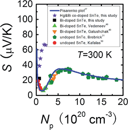 | ||
| Fig. 3 Room temperature Pisarenko plot for Sn0.98Bi0.02Te–x%HgTe samples in comparison with reported data on Bi-doped48,49 and undoped SnTe.31,50 The solid line is based on the VBM model.27 | ||
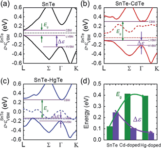
We examined this hypothesis of band convergence with DFT calculations. Fig. 4(a)–(c) show the DFT band structures of pristine SnTe, Cd-doped, and Hg-doped SnTe respectively along the lines L to Γ and Γ to K in the rocksalt BZ. It can be seen that the energy separation between the light-hole band and heavy-hole band extrema (Δε) for the Cd-doped and Hg-doped SnTe is significantly reduced relative to the pristine SnTe. Furthermore, the decrease in Δε is more pronounced in Hg-doped SnTe than in Cd-doped SnTe, consistent with our experimental observations. Moreover, the band gap, Eg, of SnTe is significantly enlarged upon Cd or Hg alloying. This band gap enlargement is beneficial to suppressing the bipolar diffusion which will be discussed later. Specifically, Δε are 0.24, 0.10, and 0.06 eV, while Eg are 0.12, 0.41, and 0.39 eV at 0 K for pure SnTe, Cd-doped, and Hg-doped SnTe respectively, as shown in Fig. 4(d). The calculated band gap of pure SnTe (0.12 eV) is in good agreement with previous calculated values (0.11 eV (ref. 51) and 0.212 eV (ref. 52)), and slightly smaller than the experimentally determined band gap (0.3 eV at 4 K (ref. 53), and 0.18 eV at 300 K (ref. 54)). Calculations of Cd-doped SnTe have been performed previously, and we find good agreement with their electronic structure.55 We find the trends in DFT-calculated band gaps and light-hole—heavy-hole energy separations agree well with the experimental observations. Specifically, we have measured electronic absorption spectra for Sn0.98Bi0.02Te–x%(Hg,Cd)Te, shown in Fig. S5.† Although specific band gaps cannot be derived from the spectra because of the strong interference from a large amount of free carriers,33 the gradual shift of the absorption edges towards higher energy region upon Hg/Cd alloying indicates an increase of band gap upon alloying.
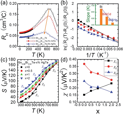
The temperature dependent Hall data analysis can further support the band convergence hypothesis. Fig. 5(a) shows the temperature dependent Hall coefficient RH for three pure phase samples Sn0.98Bi0.02Te, Sn0.98Bi0.02Te–2%HgTe, and Sn0.98Bi0.02Te–2%CdTe. RH is almost constant (less than 10% variation) below 150 K because when the temperatures are sufficiently low, almost all the charge carriers are within the light-hole band.56,57 With increasing temperature, RH increases gradually because of the temperature dependent band offset and the redistribution of carriers between the light-hole band and heavy-hole band.13,58–60 Maxima of RH, which is a sign of band convergence,13,26,61 occur around 660 K, 645 K, and 573 K for Sn0.98Bi0.02Te, Sn0.98Bi0.02Te–2%CdTe, and Sn0.98Bi0.02Te–2%HgTe, respectively. These decreased temperatures in CdTe- and HgTe-alloyed samples are indicative of diminished energy separations between the two valence bands at room temperature,26,61 which is consistent with the band structure calculations.
It is intriguing to see that the three samples have different slopes of RH–T plot. Aukerman et al.62 developed a model to analyze the high temperature Hall data of a typical two-conduction-band compound GaAs. In this model, the temperature dependent RH(T) can be expressed as:
 | (1) |
To understand the temperature dependence of the Seebeck coefficients of the Hg-alloyed samples, one can write the expressions for the diffusion Seebeck coefficient for degenerately doped semiconductors with parabolic dispersions as:57
 | (2) |
As Np increases with increasing x near room temperature (Fig. 1(c)), the increase of χ1 is mainly attributed to the enhancement of m* which can further support the band convergence hypothesis. Due to a weaker temperature dependence of RH in Hg-alloyed samples, at elevated temperature, the Np difference between Sn0.98Bi0.02Te and Hg-alloyed samples becomes more and more evident, Fig. 5(a). Under this circumstance, it is Np that dominates χ. Because of the increased Np by Hg alloying (Fig. 1(c)), χ2 and χ3 decrease with increasing x, which can well explain the lack of Seebeck coefficient enhancement in the Hg-alloyed samples at high temperatures, which is different from the case of Cd-alloyed SnTe.33
Thermal transport properties
The temperature dependent total thermal conductivities κtot for Sn0.98Bi0.02Te–x%HgTe decrease with increasing temperature and increasing amount of HgTe, Fig. 6(a). The lattice thermal conductivity κlat can be obtained by removing the electronic component κec from κtot using Wiedemann–Franz relation κec = LσT. The Lorenz number L is calculated by fitting the Seebeck coefficient data to the reduced chemical potential utilizing a single parabolic band model with acoustic phonon scattering.12,22 This yields an L with a deviation of less than 10% as compared to a more rigorous single non-parabolic band and multiple band model calculation.64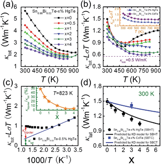 | ||
| Fig. 6 Temperature dependent (a) total thermal conductivity κtot and (b) (κtot − LσT) for Sn0.98Bi0.02Te–x%HgTe samples; the dotted line shows the theoretically lowest thermal conductivity based on the model proposed by Cahill et al.;72 inset of (b): a comparison of (κtot − LσT) between Sn0.98Bi0.02Te–2%CdTe and Sn0.98Bi0.02Te–2%HgTe; (c) an example which shows how to obtain the bipolar diffusion contribution to the total thermal conductivity by linearly fitting the (κtot − LσT) vs. 1000/T plot. Deviation of the thermal conductivity indicates a significant bipolar contribution; inset of (c): calculated κbipolar/κtot as a function of x which indicates that introduction of Hg can significantly suppress the bipolar diffusion; (d) room temperature lattice thermal conductivity κlat as a function of x. Error bars are indicated. The black and solid lines correspond to the prediction of Klemens–Drabble theory50,51 on the lattice thermal conductivity of solid solution alloys for Sn0.98Bi0.02Te–x%HgTe and Sn0.98Bi0.02Te–x%CdTe, respectively. | ||
The calculated (κtot − LσT) for Sn0.98Bi0.02Te–x%HgTe, first decreases with increasing temperature because of the phonon–phonon Umklapp scattering (U-scattering) and then increases at elevated temperature due to bipolar diffusion, Fig. 6(b). It is expected that at temperature above the Debye temperature (ΘD, ∼140 K for SnTe65), for a semiconductor with U-scattering as the dominant phonon scattering mechanism, κlat should vary as 1/T.66 The portion that deviates from such a temperature dependence can be viewed as the bipolar diffusion contribution κbipolar, Fig. 6(c). The ratio of κbipolar/κtot at 823 K as a function of x for Sn0.98Bi0.02Te–x%HgTe is illustrated in inset of Fig. 6(c). Clearly, the bipolar diffusion contribution to the total thermal conductivity decreases rapidly with increasing HgTe content, from a pronounced ∼50% for the sample with x = 0 to a negligible ∼3% for the sample with x = 4. Because of the increased hole concentration upon HgTe alloying (Fig. 1(c)) we can expect a suppression of the bipolar conduction. Therefore both the band gap opening and increase in hole concentration together are likely contributing to the suppression. That the wider band gap of the Hg containing samples contributes to the bipolar conduction suppression is evident when we compare the two samples with x = 0 and 1 having comparable hole densities (7.02 vs. 7.34 × 1020 cm−3, Fig. 1(c)). The bipolar effect in the latter is largely lowered (κbipolar/κtot decreasing from ∼50% to ∼30%, Fig. 6(c)).
The room temperature (κtot − LσT) decreases with increasing HgTe amount, which, to a large extent, is attributed to the enhanced point defect scattering induced by Hg alloying. Also, one can see from the inset of Fig. 6(b) that at comparable doping amounts the HgTe-containing sample has a lower lattice thermal conductivity than the CdTe-containing one. This is attributed to the larger atomic radius and mass difference between Hg and Sn which could cause stronger point defect scattering.
The well-accepted Klemens–Drabble (KD) model67,68 of disordered alloys was applied to predict the variation of lattice thermal conductivity of Sn0.98Bi0.02Te–x%HgTe/CdTe. The required fitting parameters are adopted from references: ΘD of 140 K,65 an average sound velocity of 1800 m s−1,69 and atomic radii for Sn, Bi, Hg, Cd, and Te in a six-coordinate environment.70 The main uncertainty in calculating lattice thermal conductivity lies in the determination of the phenomenological parameter ε which is a function of the Grüneisen parameter γ. Considering the similarity in crystal structure between SnTe and PbTe, in the present calculation, we used the same ε value (∼65) as assumed for PbTe.71
The calculated lattice thermal conductivities as a function of x in light of the KD model are shown in Fig. 6(d). For the Sn0.98Bi0.02Te–x%HgTe system, it can be seen that for the samples with x ≤ 2, within error margin, the experimental values of κlat agree well with the theoretical prediction, suggesting point defect scattering being largely responsible for the reduction of κlat. However, when x ≥ 3, the experimental κlat lies below the KD theory line, indicating other possible phonon scattering mechanisms in addition to point defect scattering, such as: mesoscale scattering via grain boundaries (GB),12 and expected GB segregation of Hg which may also contribute to phonon impedance. Interestingly, for the Sn0.98Bi0.02Te–3%CdTe, one can see that the experimental κlat is consistent with the simulated value using KD model, although PXRD unambiguously reveals the existence of CdTe second phase (Fig. S3†). Here, however, the CdTe second phase is too large in size (i.e., not nanostructured), at much lower volume fraction and too isolated to efficiently scatter acoustic phonons.
Benefiting from the enhanced alloying scattering and bipolar diffusion suppression by the Hg alloying, as well as possible contribution via interfacial scattering of phonons by GBs, the minimum κlat is only ∼0.6 Wm−1 K−1 at ∼780 K for the x = 4 sample, which is close to the theoretically lowest lattice thermal conductivity κmin (∼0.5 Wm−1 K−1) for SnTe-based material calculated using the model proposed by Cahill et al.:72
 | (3) |
Electron microscopy characterizations of Sn0.98Bi0.02Te–3%HgTe and Sn0.98Bi0.02Te–3%CdTe
The microstructure of the specimen, encompassing the crystallography, grain structure and composition analysis, was investigated by high resolution TEM (HRTEM), STEM and STEM EDS.
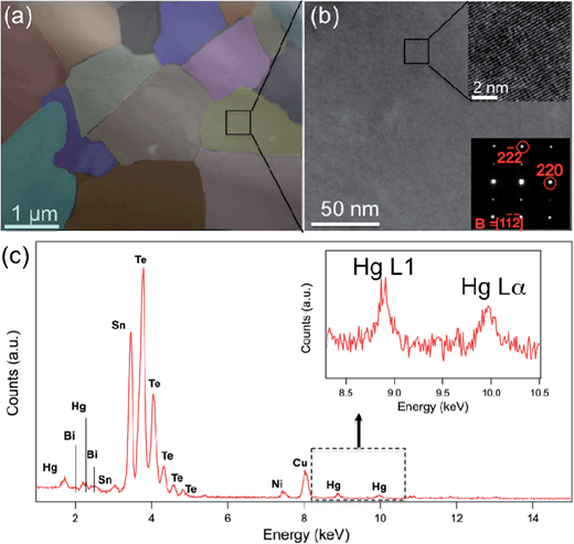
Fig. 7 shows the STEM observations of the Sn0.98Bi0.02Te–3%HgTe specimen. The presence of the meso-scale grains with size ranging from 0.4 μm to 2 μm are shown in Fig. 7(a). The meso-scale microstructure is generated by the SPS treatment. The medium magnification TEM images under varied diffraction conditions show uniform contrast, which suggests no nanoscale precipitates in the matrix. The inset figure at the upper right corner of Fig. 7(b) is a HRTEM image along [1![[1 with combining macron]](https://www.rsc.org/images/entities/char_0031_0304.gif)
![[2 with combining macron]](https://www.rsc.org/images/entities/char_0032_0304.gif) ] zone axis and the corresponding selected area diffraction (SAD) pattern is shown at the lower right corner in Fig. 7(b). However, larger size Hg-rich particles are found to preferentially occupy at the grain boundaries (and triple junctions) as shown in Fig. S6.† The occurrence of the large Hg rich particles is consistent with the PXRD result, as shown in Fig. 1(a). STEM EDS characterizes the composition of the specimen as shown in Fig. 7(c). Sn, Te, Hg and Bi peaks were identified in the spectrum. An enlarged inset figure in Fig. 7(c) shows clear Hg L1 and Lα peaks. Large Hg rich particles cannot scatter phonons effectively via interface scattering, therefore point defects scattering due to the Hg alloying is the main reason for small lattice thermal conductivity as shown in Fig. 6(b). We also note possible smaller contribution from mesoscale GB scattering and expected Hg-segregation at GBs and triple junctions. However, given microscale grain size, its contribution is likely to be smaller than the pervasive solid solution effect of Hg in SnTe.
] zone axis and the corresponding selected area diffraction (SAD) pattern is shown at the lower right corner in Fig. 7(b). However, larger size Hg-rich particles are found to preferentially occupy at the grain boundaries (and triple junctions) as shown in Fig. S6.† The occurrence of the large Hg rich particles is consistent with the PXRD result, as shown in Fig. 1(a). STEM EDS characterizes the composition of the specimen as shown in Fig. 7(c). Sn, Te, Hg and Bi peaks were identified in the spectrum. An enlarged inset figure in Fig. 7(c) shows clear Hg L1 and Lα peaks. Large Hg rich particles cannot scatter phonons effectively via interface scattering, therefore point defects scattering due to the Hg alloying is the main reason for small lattice thermal conductivity as shown in Fig. 6(b). We also note possible smaller contribution from mesoscale GB scattering and expected Hg-segregation at GBs and triple junctions. However, given microscale grain size, its contribution is likely to be smaller than the pervasive solid solution effect of Hg in SnTe.
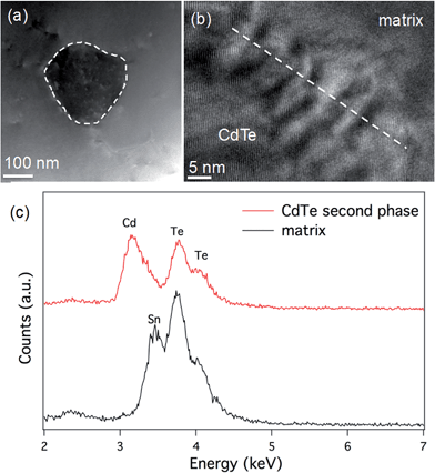
We also compare the microstructure between Sn0.98Bi0.02Te–3%HgTe and Sn0.98Bi0.02Te–3%CdTe. STEM observations of the Sn0.98Bi0.02Te–3%CdTe specimen are shown in Fig. 8. A low magnification STEM image in Fig. 8(a) shows a ∼150 nm CdTe precipitate with dark contrast embedding in the matrix, which is similar to the case in PbTe–CdTe system.61 An HRTEM image of the CdTe/matrix interface is shown in Fig. 8(b). The Moiré fringes at the interface are due to the lattice overlap of CdTe and the matrix. STEM EDS was used to reveal the composition of the CdTe second phase. Only Cd and Te signals are found in the CdTe precipitate, and no Sn peak was observed. In the matrix, the Cd peak is not observable, likely because the amount of Cd is too small to be detected by STEM EDS. The CdTe precipitates are coarse and large enough to be detected by PXRD, as shown in Fig. S3.† Also, we observe the scarce distribution and rather large size of CdTe precipitates make them inefficient at impeding the phonon propagation. This is why no obvious reduction in lattice thermal conductivity is observed when Cd exceeds its solubility limit in the Sn1.03−xCdxTe system33 and no additional lattice thermal conductivity reduction is seen when CdTe precipitates from the Sn0.98Bi0.02Te–3%CdTe sample, as shown in Fig. 6(d). The reduction in the lattice thermal conductivity of HgTe-containing SnTe (due to point defects of Hg in the SnTe matrix) is much more significant than the reduction in the lattice thermal conductivity of the CdTe-containing sample. Nevertheless, large particles of HgTe are also formed (Fig. S6†) when the solubility limits of Hg in SnTe are exceeded.
ZT values
Fig. 9(a) plots the thermoelectric figure of merit ZT as a function of temperature for Sn0.98Bi0.02Te–x%HgTe. The ZTs increase with increasing temperature and HgTe content, with the highest value reaching ∼1.35 at 923 K for the sample with x = 3. This is ∼50% improvement over the pristine Sn0.98Bi0.02Te sample and 30% higher than that of Sn0.98Bi0.02Te–3%CdTe (ZT ∼ 1.05 at 870 K). This enhancement of ZT mainly originates from the significantly improved power factor and greatly lowered lattice thermal conductivity via HgTe alloying. This value is also slightly higher than what we obtained in the SnCd0.03Te–x%CdS system33 and much superior to that of In-doped SnTe.27 More importantly, a great enhancement of ZTave has been achieved. Specifically, the ZTave values between 300 and 900 K are 0.55, 0.71, and 0.84 for In-doped SnTe, SnCd0.03Te–2%CdS, and Sn0.98Bi0.02Te–3%HgTe, respectively, while those between 500 and 900 K are 0.72, 0.87, and 1.02, respectively, Fig. 9(b). This is comparable to the ZTave of the recently reported SnSe single crystals for the same temperature range.73 We note that a significant enhancement of ZTave is of greater value to overall thermoelectric conversion efficiency than just increasing the maximum value of ZT.74 Although we have not performed systematic studies, we found that the high performance material is quite stable even after heating at 723 K for 7 d in vacuum, see Fig. S7.†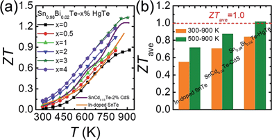 | ||
| Fig. 9 (a) Temperature dependent ZT values for Sn0.98Bi0.02Te–x%HgTe and Sn0.98Bi0.02Te–3%CdTe in comparison with the reported data on In-doped SnTe27 and Cd-doped SnTe nanostructured with CdS;33 (b) a comparison of average ZT (ZTave) of 300–900 K and 500–900 K among In-doped SnTe,27 SnCd0.03Te–2%CdS,33 and Sn0.98Bi0.02Te–3%HgTe. | ||
4. Concluding remarks
The introduction of Hg in the Sn-site of SnTe is effective in achieving valence band convergence, giving rise to a great enhancement of the Seebeck coefficient and the power factor. Due to the large differences in atomic radii and mass contrast between Hg and Sn, strong point defect scattering is apparent upon HgTe alloying, which along with contributions from mesoscale GBs results in a noticeable reduction of lattice thermal conductivity. In conjunction with the bipolar diffusion suppression due to band gap opening by Hg alloying, the Sn0.98Bi0.02Te–x%HgTe system possesses a very low lattice thermal conductivity. The multiply favorable roles that Hg plays in regulating the electron and phonon transport of SnTe lead to a maximum ZT of 1.35 at ∼910 K and more importantly, a largely enhanced average ZT in Sn0.98Bi0.02Te–x%HgTe. This work suggests that SnTe-based materials are viable candidates for thermoelectric power generation.Acknowledgements
This work was supported as part of the Revolutionary Materials for Solid State Energy Conversion, an Energy Frontier Research Center funded by the U.S. Department of Energy, Office of Science, and Office of Basic Energy Sciences under Award Number DE-SC0001054. Transmission electron microscopy work was partially performed in the EPIC facility of the NUANCE Center at Northwestern University.References
- (a) F. J. DiSalvo, Science, 1999, 285, 703–706 Search PubMed; (b) L.-D. Zhao, V. P. Dravid and M. G. Kanatzidis, Energy Environ. Sci., 2014, 7, 251–268 RSC; (c) J. He, M. G. Kanatzidis and V. P. Dravid, Mater. Today, 2013, 16, 166–176 Search PubMed.
- (a) L. E. Bell, Science, 2008, 321, 1457–1461 Search PubMed; (b) M. G. Kanatzidis, Chem. Mater., 2010, 22, 648–659 Search PubMed.
- T. M. Tritt, Science, 1999, 283, 804–805 CrossRef CAS.
- J. Yang and T. Caillat, MRS Bull., 2006, 31, 224–229 Search PubMed.
- F. Rosi, Solid-State Electron., 1968, 11, 833–868 Search PubMed.
- J.-P. Fleurial, JOM, 2009, 61, 79–85 CrossRef CAS.
- T. D. Barr and F. Dahlen, J. Geophys. Res.: Solid Earth, 1989, 94, 3923–3947 Search PubMed.
- C.-T. Hsu, G.-Y. Huang, H.-S. Chu, B. Yu and D.-J. Yao, Appl. Energy, 2011, 88, 1291–1297 Search PubMed.
- C. Wu, Appl. Therm. Eng., 1996, 16, 63–69 Search PubMed.
- K. F. Hsu, S. Loo, F. Guo, W. Chen, J. S. Dyck, C. Uher, T. Hogan, E. Polychroniadis and M. G. Kanatzidis, Science, 2004, 303, 818–821 Search PubMed.
- J. P. Heremans, V. Jovovic, E. S. Toberer, A. Saramat, K. Kurosaki, A. Charoenphakdee, S. Yamanaka and G. J. Snyder, Science, 2008, 321, 554–557 Search PubMed.
- K. Biswas, J. He, I. D. Blum, C.-I. Wu, T. P. Hogan, D. N. Seidman, V. P. Dravid and M. G. Kanatzidis, Nature, 2012, 489, 414–418 Search PubMed.
- Y. Pei, X. Shi, A. LaLonde, H. Wang, L. Chen and G. J. Snyder, Nature, 2011, 473, 66–69 Search PubMed.
- R. J. Korkosz, T. C. Chasapis, S.-H. Lo, J. W. Doak, Y. J. Kim, C.-I. Wu, E. Hatzikraniotis, T. P. Hogan, D. N. Seidman and C. Wolverton, J. Am. Chem. Soc., 2014, 136, 3225–3237 CrossRef CAS PubMed.
- J. Androulakis, I. Todorov, J. He, D.-Y. Chung, V. Dravid and M. Kanatzidis, J. Am. Chem. Soc., 2011, 133, 10920–10927 Search PubMed.
- J. R. Sootsman, H. Kong, C. Uher, J. J. D'Angelo, C. I. Wu, T. P. Hogan, T. Caillat and M. G. Kanatzidis, Angew. Chem., 2008, 120, 8746–8750 Search PubMed.
- L.-D. Zhao, J. He, C.-I. Wu, T. P. Hogan, X. Zhou, C. Uher, V. P. Dravid and M. G. Kanatzidis, J. Am. Chem. Soc., 2012, 134, 7902–7912 Search PubMed.
- B. Sales, D. Mandrus and R. K. Williams, Science, 1996, 272, 1325–1328 CrossRef CAS.
- X. Shi, J. Yang, J. R. Salvador, M. Chi, J. Y. Cho, H. Wang, S. Bai, J. Yang, W. Zhang and L. Chen, J. Am. Chem. Soc., 2011, 133, 7837–7846 Search PubMed.
- G. Rogl, A. Grytsiv, P. Rogl, N. Peranio, E. Bauer, M. Zehetbauer and O. Eibl, Acta Mater., 2014, 63, 30–43 Search PubMed.
- Y. Qiu, L. Xi, X. Shi, P. Qiu, W. Zhang, L. Chen, J. R. Salvador, J. Y. Cho, J. Yang and Y. C. Chien, Adv. Funct. Mater., 2013, 23, 3194–3203 Search PubMed.
- G. Tan, W. Liu, H. Chi, X. Su, S. Wang, Y. Yan, X. Tang, W. Wong-Ng and C. Uher, Acta Mater., 2013, 61, 7693–7704 Search PubMed.
- J. Yao, N. J. Takas, M. L. Schliefert, D. S. Paprocki, P. E. Blanchard, H. Gou, A. Mar, C. L. Exstrom, S. A. Darveau and P. F. Poudeu, Phys. Rev. B: Condens. Matter Mater. Phys., 2011, 84, 075203 Search PubMed.
- J. Y. Cho, X. Shi, J. Salvador, J. Yang and H. Wang, J. Appl. Phys., 2010, 108, 073713 Search PubMed.
- R. Liu, L. Xi, H. Liu, X. Shi, W. Zhang and L. Chen, Chem. Commun., 2012, 48, 3818–3820 RSC.
- L. Zhao, H. Wu, S. Hao, C. Wu, X. Zhou, K. Biswas, J. He, T. Hogan, C. Uher and C. Wolverton, Energy Environ. Sci., 2013, 6, 3346–3355 CAS.
- Q. Zhang, B. Liao, Y. Lan, K. Lukas, W. Liu, K. Esfarjani, C. Opeil, D. Broido, G. Chen and Z. Ren, Proc. Natl. Acad. Sci. U. S. A., 2013, 110, 13261–13266 Search PubMed.
- Y. Chen, M. D. Nielsen, Y. B. Gao, T. J. Zhu, X. Zhao and J. P. Heremans, Adv. Energy Mater., 2012, 2, 58–62 Search PubMed.
- D. J. Singh, Funct. Mater. Lett., 2010, 3, 223–226 Search PubMed.
- M. K. Han, J. Androulakis, S. J. Kim and M. G. Kanatzidis, Adv. Energy Mater., 2012, 2, 157–161 Search PubMed.
- R. Brebrick and A. Strauss, Phys. Rev., 1963, 131, 104 CrossRef.
- S. Rabii, Phys. Rev., 1969, 182, 821 Search PubMed.
- G. Tan, L.-D. Zhao, F. Shi, J. W. Doak, S.-H. Lo, H. Sun, C. Wolverton, V. P. Dravid, C. Uher and M. G. Kanatzidis, J. Am. Chem. Soc., 2014, 136, 7006–7017 CrossRef CAS PubMed.
- P. Hohenberg and W. Kohn, Phys. Rev., 1964, 136, B864 Search PubMed.
- W. Khon and L. Sham, Phys. Rev., 1965, 140, A1133–A1138 Search PubMed.
- G. Kresse and J. Hafner, Phys. Rev. B: Condens. Matter Mater. Phys., 1993, 47, 558 Search PubMed.
- G. Kresse and J. Hafner, Phys. Rev. B: Condens. Matter Mater. Phys., 1994, 49, 14251 Search PubMed.
- G. Kresse and J. Furthmüller, Phys. Rev. B: Condens. Matter Mater. Phys., 1996, 54, 11169 Search PubMed.
- G. Kresse and J. Furthmüller, Comput. Mater. Sci., 1996, 6, 15–50 Search PubMed.
- P. E. Blöchl, Phys. Rev. B: Condens. Matter Mater. Phys., 1994, 50, 17953 Search PubMed.
- J. P. Perdew, K. Burke and M. Ernzerhof, Phys. Rev. Lett., 1996, 77, 3865 Search PubMed.
- G. Kresse and D. Joubert, Phys. Rev. B: Condens. Matter Mater. Phys., 1999, 59, 1758 CrossRef CAS.
- J. E. Saal, S. Kirklin, M. Aykol, B. Meredig and C. Wolverton, JOM, 2013, 65, 1501–1509 CrossRef CAS PubMed.
- S. Lany and A. Zunger, Modell. Simul. Mater. Sci. Eng., 2009, 17, 084002 Search PubMed.
- Y. N. Nasirov, N. Sultanova and T. Osmanov, Phys. Status Solidi B, 1969, 35, K39–K42 Search PubMed.
- K. Biswas, J. He, G. Wang, S.-H. Lo, C. Uher, V. P. Dravid and M. G. Kanatzidis, Energy Environ. Sci., 2011, 4, 4675–4684 CAS.
- J. Androulakis, Y. Lee, I. Todorov, D.-Y. Chung and M. Kanatzidis, Phys. Rev. B: Condens. Matter Mater. Phys., 2011, 83, 195209 Search PubMed.
- V. P. Vedeneev, S. P. Krivoruchko and E. P. Sabo, Semiconductors, 1998, 32, 241–244 Search PubMed.
- M. Galushchak, D. Freik, I. Ivanyshyn, A. Lisak and M. Pyts, J. Thermoelectr., 2000, 42–50 CAS.
- J. Kafalas, R. Brebrick and A. Strauss, Appl. Phys. Lett., 1964, 4, 93–94 Search PubMed.
- N. Wang, D. West, J. Liu, J. Li, Q. Yan, B.-L. Gu, S. Zhang and W. Duan, Phys. Rev. B: Condens. Matter Mater. Phys., 2014, 89, 045142 Search PubMed.
- C. Okoye, J. Phys.: Condens. Matter, 2002, 14, 8625 Search PubMed.
- L. Esaki and P. Stiles, Phys. Rev. Lett., 1966, 16, 1108 CrossRef.
- J. Dimmock, I. Melngailis and A. Strauss, Phys. Rev. Lett., 1966, 16, 1193 Search PubMed.
- The electronic DOS of Cd-doped SnTe has been previously calculated, where it was also found that the Cd defect opened the band gap of SnTe and created an impurity band within the band gap of SnTe [S. Ahmad, Adv. Mater. Res., 2013, 701, 125]. However, they incorrectly placed the Fermi level of the calculation above this impurity level, suggesting that the Cd impurity band should be filled. In contrast, we find that the Fermi level [dotted line in Fig. 4(b)] lies below the impurity band [dashed line in Fig. 4(b)], suggesting that the effects of Cd on the transport properties of SnTe should be related to the modification of the valence band, as opposed to resonant-level enhancement [J. P. Heremans et al., Science, 2008, 321, 554–557].
- R. S. Allgaier and B. B. Houston, J. Appl. Phys., 1966, 37, 302–309 Search PubMed.
- I. U. R. I. Ravich, B. A. E. Efimova and I. A. Smirnov, Semiconducting lead chalcogenides, Plenum Publishing Corporation, 1970 Search PubMed.
- A. Andreev and V. Radionov, Soviet Physics Semiconductors, 1967, 1, 145–148 Search PubMed.
- I. Chernik, V. Kaidanov, M. Vinogradova and N. Kolomoets, Soviet Physics Semiconductors, 1968, 2, 645–651 Search PubMed.
- J. Androulakis, I. Todorov, D.-Y. Chung, S. Ballikaya, G. Wang, C. Uher and M. Kanatzidis, Phys. Rev. B: Condens. Matter Mater. Phys., 2010, 82, 115209 Search PubMed.
- Y. Pei, A. D. LaLonde, N. A. Heinz and G. J. Snyder, Adv. Energy Mater., 2012, 2, 670–675 Search PubMed.
- L. Aukerman and R. Willardson, J. Appl. Phys., 1960, 31, 939–940 Search PubMed.
- Y. Pei, A. LaLonde, S. Iwanaga and G. J. Snyder, Energy Environ. Sci., 2011, 4, 2085–2089 CAS.
- M. Vinograd, N. Kolomoet, I. Smirnov and L. Sysoeva, Soviet Physics Semiconductors, 1968, 9, 2368 Search PubMed.
- S. Bukshpan, Solid State Commun., 1968, 6, 477–478 Search PubMed.
- G. S. Nolas, J. Sharp and J. Goldsmid, Thermoelectrics: basic principles and new materials developments, Springer, 2001 Search PubMed.
- T. Irie, Jpn. J. Appl. Phys., 1966, 5, 854–859 Search PubMed.
- J. Yang, G. Meisner and L. Chen, Appl. Phys. Lett., 2004, 85, 1140–1142 Search PubMed.
- P. Bauer Pereira, I. Sergueev, S. Gorsse, J. Dadda, E. Müller and R. P. Hermann, Phys. Status Solidi B, 2013, 250, 1300–1307 CrossRef CAS.
- R. Shannon, Acta Crystallogr., Sect. A: Found. Crystallogr., 1976, 32, 751–767 Search PubMed.
- G. Alekseeva, B. Efimova, L. Ostrovskaya, O. Serebryannikova and M. Tsypin, Soviet Physics Semiconductors, 1971, 4, 1122–1125 Search PubMed.
- D. G. Cahill, S. K. Watson and R. O. Pohl, Phys. Rev. B: Condens. Matter Mater. Phys., 1992, 46, 6131 Search PubMed.
- L.-D. Zhao, S.-H. Lo, Y. Zhang, H. Sun, G. Tan, C. Uher, C. Wolverton, V. P. Dravid and M. G. Kanatzidis, Nature, 2014, 508, 373–377 Search PubMed.
- H. J. Wu, L. D. Zhao, F. S. Zheng, D. Wu, Y. L. Pei, X. Tong, M. G. Kanatzidis and J. He, Nat. Commun., 2014, 5, 4515 CAS.
Footnotes |
| † Electronic supplementary information (ESI) available: Room temperature densities for all the samples investigated in this study (Table S1); powder XRD pattern of as-synthesized HgTe (Fig. S1); thermal diffusivity, heat capacity, and Lorenz number for Sn0.98Bi0.02Te–x%HgTe/CdTe samples (Fig. S2); powder XRD pattern of Sn0.98Bi0.02Te–x%CdTe (Fig. S3); temperature dependent thermoelectric transport properties for Sn0.98Bi0.02Te–x%CdTe (Fig. S4); Electronic absorption spectra for Sn0.98Bi0.02Te–x%(Hg,Cd)Te (Fig. S5); STEM EDS spectrum image of Sn0.98Bi0.02Te–3%HgTe (Fig. S6); temperature dependent thermoelectric transport properties for Sn0.98Bi0.02Te–3%HgTe before and after a 723 K–7 d vacuum annealing treatment (Fig. S7). See DOI: 10.1039/c4ee01463d |
| ‡ G.J.T. and M.G.K. conceived of and planned the experiments. G.J.T. synthesized the samples, carried out and analyzed thermoelectric experiments. F.Y.S. and V.P.D. performed the TEM characterizations J.W.D. and C.W. carried out the band structure calculations. H.S. and C.U. carried out the Hall measurements. L.D.Z. and P.L.W. helped with sample synthesis. G.J.T., F.Y.S., J.W.D., H.S., L.D.Z., P.L.W., C.U., C.W., V.P.D. and M.G.K. conceived the experiments, analyzed the results and co-edited the manuscript. |
| This journal is © The Royal Society of Chemistry 2015 |

