
Consistent double Gaussian model with non-symmetric potential barriers at contacts for organic diodes
Muhammad Ammar Khana,
Sun Jiu-Xun*ab,
Jin Keb,
Cai Ling-Cangb and
Wu Qiangb
aSchool of Physical Electronics, University of Electronic Science and Technology, Chengdu 610054, China. E-mail: sjx@uestc.edu.cn
bLaboratory for Shock Wave and Detonation Physics Research, Southwest Institute of Fluid Physics, Mianyang 621900, China
First published on 26th September 2014
Abstract
A transport model with double Gaussian density of state (DOS) for organic semiconductors is proposed, with one Gaussian DOS for free carriers and one for trapped carriers. The variations of the density of trapped carriers with the density of free carriers, the effective mobility and the ratio of diffusion coefficient to effective mobility with the density of trapped carriers are analyzed. It is shown that the ratio of diffusion coefficient to effective mobility is the Einstein type for free carriers, but the ratio for total carriers is the non-Einstein type, and is an increasing function of the density of trapped carriers at low density, and a decreasing function at high density. The importance of non-symmetric barriers at contacts is emphasized to quantitatively describe the current–voltage relationships of typical organic layers sandwiched between two metallic electrodes. It is shown that slopes of current–voltage curves at low bias are very sensitive to the values of right barriers. The slopes in all bias are sensitive to the values of left barriers, and increase as the left barrier decreases. When applying the modified model to three organic diodes, an excellent agreement is obtained between theoretical results and experimental data.
1. Introduction
The research of optoelectronic and electrical transport properties in conjugated semiconducting polymers has drawn intensive attention because of their potential applications in organic semiconductor devices such as light-emitting diodes (LEDs) and field-effect transistors (FETs).1–18 Understanding their charge-carrier transport properties is very useful to improving the devices' performances, and to designing and synthesizing better materials. It was demonstrated that the current in single carrier diodes with amorphous polymer layers sandwiched by two electrodes is space-charge limited (SCL).1–18Davids et al.1 proposed a unified device model considering two types of carriers for single layer organic LEDs, and Crone et al.2 extended it into bilayer diodes. They also studied the impact of local electric fields on the injection barrier. Koster et al.3 proposed a model for organic solar cells considering two types of carriers. However, most organic diodes have a single type of carrier, and the SCL current in organic diodes is described by the solutions of drift and Poisson equations, with different expressions of mobility. The density dependent mobility of Vissenberg and Matters (VM)4 is popular, which originates from hopping in an exponential density of states (DOS). This description has been used to unify the charge transport in FETs and LEDs.5–7 Pasveer et al.8 developed a description for the mobility incorporating both the density and field dependence, based on charge-carrier hopping within the Gaussian DOS. The mobility of Pasveer et al. has been widely applied to describe current–voltage (J–V) relationships of organic devices by many authors.9–18
van Mensfoort et al.11 and we12,13 have numerically solved the drift–diffusion model (DDM) and drift model by using parameters optimized by Pasveer et al.8 for NRS-PPV and OC1C10-PPV. The obtained J–V curves are in good agreement with experimental data.9–13 Zhou et al.14 studied the effect of high carrier density on mobility by using the Monte Carlo simulation. Coehoorn et al.,15,16 and Bässler and Köhler17 reviewed recent advances in charge transport in disordered organic semiconductors. Myers and Xue18 reviewed organic semiconductors and their applications in photovoltaic devices. They discussed the fundamental electronic nature of organic semiconductors, processing techniques, and their application to two main classes of optoelectronic devices: light emitting diodes, and photovoltaics.
However, Zhang et al.19 demonstrated that electron transport is consistently described by the concept of free electrons in combination with deep traps. Recently Nicolai et al.20,21 analyzed the reason that both the VM and Pasveer models provide a consistent description of the J–V relationships of organic devices. The reason is that the section of the Gaussian DOS that is being filled during a J–V scan may also be approximated by an exponential distribution, or vice versa.20,21 Nicolai et al.20,21 further emphasized that the trapped carriers are very important for description of J–V curves. If considering the trapped carriers with Gaussian DOS in the DDM and treating the mobility as a constant, the J–V curves of many organic diodes can be qualitatively described. However, the fitting procedure and values of parameters are not clearly presented and explained.20,21
Lange et al.22 proposed a model for band bending in contacts of polymer layers with metallic electrodes. Cottaar et al.23,24 presented a scaling theory for charge transport in disordered molecular semiconductors that extends percolation theory to the random resistor network representing charge hopping. A density dependent mobility for Miller–Abrahams and Marcus hopping on different lattices with Gaussian energy disorder was derived. Oelerich et al.25 suggested a recipe for determining the density of states (DOS) in disordered organic semiconductors from the measured dependence of the charge carrier mobility on the concentration of carriers. The recipe is based on a theory for the concentration-dependent mobility. Fishchuk et al.26 developed an analytical mobility model to describe hopping transport in organic semiconductors including both energetic disorder and polaronic contributions due to geometric relaxation.
Bruyn et al.27 derived an analytic approximate JV formula for organic diodes. In the derivation of the analytic formula, mobility was treated as a function of temperature, being independent of density and electric field. However, the analytic formula cannot consider trapped carriers, and it merely describes JV data qualitatively. It is notable that Pasveer et al.,5 Bruyn et al.,27 and Nicolai et al.20,21 all belong to the group of Blom. They have proposed tens of models considering different physical effects, but the final model has not been found.3,5,8,19–21,27,42
Except for the traps, the barriers at contacts between organic layers and electrodes are important for quantitative descriptions of JV data. Davids et al.1 and Crone et al.2 studied the impact of local electric fields on the injection barrier. Chen et al.28 studied the electrostatic field and partial Fermi level pinning at the pentacene–SiO2 interface. Recently, Yogev et al.29 and Oehzelt et al.30 independently proposed that Fermi level pinning is induced by gap states in organic semiconductors. Because the height of barriers is tightly related to Fermi levels, and since the Fermi level in organic semiconductors is pinned, it implies that the barriers are almost constant. Neumann et al.31,32 developed a self-consistent theory of unipolar charge-carrier injection in metal/insulator/metal systems. They derived boundary conditions used for the drift–diffusion equations. The densities of electrons31 or holes32 were expressed as functions of barriers which were weakly dependent on electric field at interfaces. Thus, Bruyn et al.27 directly adopted constant barriers in their derivation of an analytic JV formula.
In the DDM, the ratio between the diffusion coefficient D and the mobility μ is given by the Einstein relationship (ER), D/μ = kBT/q. Some authors33–36 have proposed that the ER should be replaced by the generalized Einstein relation (GER) with the ratio kBT/q multiplied by a factor. However, Neumann et al.37 have disproved the GER through theoretical analysis. Wetzelaer et al.38 confirmed the validity of the ER in organic semiconductors by studying the diffusion-driven currents of single-carrier diodes.
In this paper, we present a detailed formulation of the DDM with Gaussian traps taken into account, give an explanation of the GER, and show that, except for Gaussian traps, the non-symmetric potential barriers at contacts are important factors for the quantitative description of J–V curves. Our work applies the DDM to three typical diodes.
2. Fundamental model
The fundamental energy-band model for p-type materials used in this paper is schematically plotted in Fig. 1. The model in Fig. 1 consists of two Gaussian DOS. One Gaussian DOS exists for free carriers and one exists for trapped carriers with widths σ and σt, and center energy levels Ev and Et, respectively.
 | (1) |
 | (2) |
 | (3) |
 | (4) |
| f(E) = {1 + exp[(EF − E + qφ(x))/kBT]}−1 ≡ {1 + exp[(EF(x) − E)/kBT]}−1 | (5) |
 | ||
| Fig. 1 Schematic diagram of the energy-band model proposed in this paper. | ||
Here f(E) is the Fermi–Dirac (FD) distribution function, EF is the Fermi energy level without an external electric field, and EF(x) = EF + qφ(x) is the quasi-Fermi energy level. There is no constant EF(x) in a device under SCL conditions, but the separated EF should be a constant.
It should be pointed out that although the same FD distribution f(E) is used in both eqn (3) and (4), the literature20,21 shows that the Einstein relationship is valid for organic semiconductors. This implies that the organic semiconductors should be non-degenerate, (EF − Ev) ≫ kT. Therefore, the position of EF is near Et and deviated from Ev in Fig. 1. The boundary conditions in eqn (16) and (17) show that φ(x) > 0, so even under SCL conditions, the quasi-Fermi energy EF(x) also satisfies the non-degenerate condition, (EF(x) − Ev) ≫ kT. This means that the free holes can be seen as non-degenerate, and the trapped holes should be treated as degenerate. The Fermi–Dirac distribution in eqn (4) can and cannot be approximated by the Boltzmann distribution as applied to free holes and trapped holes, respectively. eqn (3) for free holes can be simplified as follows
 | (6) |
Defining the effective DOS
 | (7) |
| pf = Nf exp[(−qφ(x))/kT] | (8) |
Introducing the dimensionless variable,  , we can evaluate the integral in eqn (7)

| Nf = N0 exp[(Ev − EF)/kT]exp[σ2/2(kT)2] | (9) |
| f(E) ≈ {1 + (Nf/pf)exp[(EF − E)/kBT]}−1 | (10) |
One easy misunderstanding is that to derive eqn (8), the Fermi–Dirac distribution is approximated by a Boltzmann distribution and then this result is substituted in the Fermi–Dirac statistics in eqn (5) to arrive at eqn (10). This treatment is correct, and we explain the reason in more detail. The original Fermi distribution eqn (5) is applicable to both free and trapped holes, but the Boltzmann approximation in eqn (8) merely applies to free holes. However, as the transformed eqn (10) is applied to free holes, we may obtain the identity, pf = pf. Therefore there is no contradiction in eqn (10).
Nicolai et al.20,21 pointed out that the trapped holes can be easily realized in the program based on the discretization method of Gummel and Scharfetter,39,40 if the Dt(E) for trapped holes is taken as the single trap model. In contrast, the Fermi integral in eqn (4) with Gaussian DOS is not easy to realize.20,21 It is necessary to use the accurate approximation of the Gauss–Fermi integral recently reported by Paasch and Scheinert.41 By using their approximation,41 the effect of Gaussianly-distributed traps on the transport can be accessed. However, from eqn (10), we can derive the following expression
| pf(∂f/∂pf) = {1 + (Nv/pf)exp[(EF − E)/kBT]}−2(Nf/pf)exp[(EF − E)/kBT] | (11) |
Substitution of eqn (10) into eqn (11) yields
| pf(∂f/∂pf) = f2(f−1 − 1) = f(1 − f) | (12) |
Then the derivatives of trapped charges with respect to the free charges can be easily evaluated as
 | (13) |
By combining eqn (13) with the discretization method of Gummel and Scharfetter,39,40 the Gauss–Fermi integral can be easily and directly realized in the program, without the need for the approximation of Paasch and Scheinert.41
With trapped charges taken into account, the Poisson equation is as follows
 | (14) |
Considering that the trapped charges do not contribute to current, and supposing a constant mobility, the drift–diffusion equation takes the following form
 | (15) |
In order to solve eqn (14) and (15), we need to use eqn (4), (8) and (10).
Assuming the thickness of the organic layer is L, the left-side contact (x = 0) can be seen as Ohmic with a low potential barrier Wleft. The right-side contact (x = L) can be seen as Schottky with a high potential barrier Wright. The difference between right and left potential barriers, Vbi = Wright − Wleft, is the built-in potential in the devices. The boundary conditions for the Poisson equation is as follows27
| φ(0) = Wleft + V, φ(L) = Wright | (16) |
| V − Vbi = φ(0) − φ(L) | (17) |
For the boundary conditions for the drift–diffusion equations, Neumann et al.31,32 have derived the following equations
 | (18a) |
 | (18b) |
 | (19) |
The typical values of parameters in eqn (19) are as follows, n∞ ≈ 4 eV, E∞ ≈ 3 × 1028 m3, and l ≈ 7.088 × 10⁻¹¹ m. In the devices studied in this paper, the values of F(0) and F(L) are about 103 and 107 (V m−1), respectively. The values of εrqlleftF(0) and εrqlrightF(L) are about 10−6 and 10−2 eV, respectively. The second terms in the exponential functions of eqn (18) can be neglected as compared with the first terms. Therefore eqn (18) can be simplified to the following form27
| pf(0) = Nf exp(−Wleft/kT), pf(L) = Nf exp(−Wright/kT) | (20) |
The boundary conditions in eqn (16) and (20) have been used by Bruyn et al.27
Ahead of concrete calculations, it is necessary to explain that our model goes beyond those proposed in previous publications. Firstly, Nicolai et al.20,21 adopted the program of Koster et al.;3 they did not consider potential barriers at contacts, and adopted symmetric Ohmic contacts with Wleft = Wright, as mentioned in last line of page 2 in their paper.20 Our calculations show that asymmetric contacts with different barriers are very important to improve the fitting quality of experimental J–V data. Secondly, Nicolai et al.20,21 did not mention boundary conditions used for the drift–diffusion equations. Thirdly, they did not use the non-degenerate condition for free holes, and did not extract effective DOS as a function of temperature. They also did not extract the temperature function of mobility. Fourthly, they did not derive relationships in eqn (11)–(13) ; they used an approximation of the Gauss–Fermi integral as proposed by Paasch and Scheinert.41
3. Analysis
Eqn (4), (8), (10), (14) and (15) show that the calculation of trap-limited currents requires a separation of the total carrier density into free (pf) and trapped (pt) carriers. We plot the (pt–pf) relationship with different values of σ in Fig. 2. The figure also shows that the influence of σ to (pt–pf) curves is very prominent. The pt is always an increasing function of pf and σ. The slopes of (pt–pf) curves are large when pf is low and σ is small; the slopes decrease as pf and σ increase. The pt would reach saturation at high pf. There exists a cross point of pf for all curves, such that at this value of pf, all curves have the same value of pt. | ||
| Fig. 2 Schematic diagram for the (pt–pf) relationship calculated by using eqn (4) and (10) at 300 K, with Nf = 1026 m−3, Nt = 1023 m−3, EtF = 0.3 eV, and with different values of σt; σt = 0, 0.05, 0.1, 0.15, 0.2 eV, respectively. The calculations in this figure do not involve the Gaussian width σ of free holes. | ||
Now we give a qualitative explanation of the increase of mobility and GER based on trapped charges. For simplicity, we just consider the single trap case. In terms of eqn (4) and (10), if a single trap level Et is assumed, the density of trapped charges can be expressed as
| pt = Ntf(Et) = Nt{1 + (Nf/p)exp[(EF − Et)/kBT]}−1 | (21) |
In the situation considering GER, it is not necessary to divide the carriers into free and trapped types. We may introduce total density of carriers
| p = pf + pt | (22) |
The Poisson and DD equations can then be reformulated by using p
 | (23) |
 | (24) |
The substitution of eqn (21) into eqn (22) results in the quadratic equation for pf
| pf2 − pf(p − Nt − Nq) − pNq = 0 | (25) |
The solution is as follows
| pf = (1/2)(p − Nt − Nq) + (1/2)[(p − Nt − Nq)2 + 4Nqp]1/2 | (26) |
| Nq = Nf exp[(EF − Et)/kBT] | (27) |
Its derivative can be evaluated as
 | (28) |
By substituting eqn (26) and (28) into eqn (14) and (15), and comparing the resulting equation with eqn (23) and (24), we obtain the effective mobility and diffusion coefficient.
 | (29) |
 | (30) |
It should be pointed out that trap-modulated mobilities were introduced decades ago,1,2,4,23–26 although not within the Gaussian DOS leading to eqn (29), and there are many possible GERs, for example field-depend mobility.33–37
Eqn (29) shows that although the mobility μ0 in the original model in eqn (14) and (15) is a constant, where the carriers are divided into free and trapped types, the effective mobility μ and diffusion coefficient D in the transformed eqn (24) become functions of density of carriers. In Fig. 3, we plot the relationships of μ and D/μ with p. The figure shows that μ is an increasing function of p, and the increase becomes more dramatic as the depth of traps increases. This tendency is in agreement with that of VM theory.4–7 The VM theory does not divide the carriers into free and trapped, and expresses μ as a function of density of carriers.
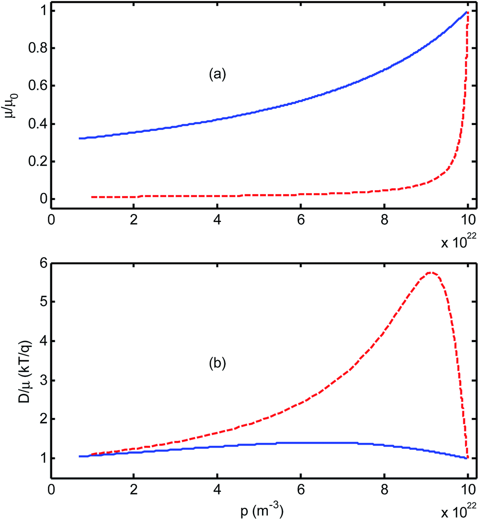 | ||
| Fig. 3 The qualitative (μ–p) and (D/μ–p) relationships calculated by using eqn (26)–(30) at 300 K, with Nf = 1026 m−3, Nt = 1023 m−3, EtF = 0.2 eV (solid lines) and 0.3 eV (dashed lines), and with σt = 0 eV. The calculations in this figure do not involve the Gaussian width σ of free holes. | ||
Based on the analysis, one may deduce following assumption that the trapped carriers is equivalent to effective mobility as a function of carrier density; both factors cannot be considered at same time. The latest works of Zhang et al.19 and Nicolai et al.20,21 also consider this situation. Since they consider trapped charges in their model,19–21 they treat mobility as a constant, and do not use the mobility model of Pasveer et al.8 which treats mobility as a function of density of carriers and electric field. Both authors belong to same research group led by Blom.8,19–21
Fig. 3 also shows that the ratio of D/μ deviates from the ER value kT/q, and the GER appears. However, the ratio also differs from the one in previous references,33–35 in which the GER is due to degenerate effect of carriers. Since the viewpoint on GER is controversial in literature,33–36 and the latest experiment37 supports the ER for free carriers, the theoretical model dividing carriers into free and trapped types is consistent with the experiment.37
The model of Nicolai et al.20,21 does not consider the asymmetric barriers at contacts, and adopted symmetric Ohmic contacts with Wleft = Wright.20 In our calculations, it is shown that the potential barriers have a severe impact on the shape of J–V curves. In Fig. 4 we plot several J–V curves with different values of Wleft and Wright. The figure shows that keeping Wleft constant and increasing Wright causes the J–V curves to bend down dramatically at low voltage. Keeping Wright constant and increasing Wleft causes the J–V curves to move down and the slope to slightly decrease. Therefore it is necessary to adjust values of Wleft and Wright to fit the shapes of J–V curves.
 | ||
| Fig. 4 The J–V curves calculated at 300 K, with μ0 = 2 × 10⁻¹⁰ m2 V−1 s−1, Nt = 2 × 10²² m−3, σ = 0.1 eV, and EtF = 0.22 eV. (a) Wleft = 0.1 eV, and Wright = (0.1, 0.3, 0.5, 0.7, 0.9) eV. (b) Wright = 0.1 eV, and Wleft = (0.1, 0.3, 0.5, 0.7, 0.9) eV. | ||
4. Application to devices
Now we apply the above Gaussian model to polymer layers of poly[4′-(3,7-dimethyloctyloxy)-1,1′-biphenylene-2,5-vinylene] (NRS-PPV), poly(2-methoxy-5-(3′,7′-dimethyloctyloxy)-p-phenylene-vinylene) (OC1C10-PPV),8,10 and poly(3-hexylthiophene) (P3HT),5,42 with thicknesses of L = 560 nm, 275 nm and 95 nm respectively. In Fig. 5–7, we plot J–V curves for the three materials for comparison with experimental points. The three figures show that the agreement of theoretical curves with experimental J–V points is fairly good. For the three devices studied in this work, the agreement is quantitative for every isothermal line, with respect to the shapes and slopes from low to high voltage ranges, and also the values of current at every point within wide varying ranges, from 10−6 to 1, 10−5 to 1 and 10−19 to 1 A m−2 for NRS-PPV, OC1C10-PPV and P3HT devices, respectively. Because the works of Nicolai et al.20,21 do not consider non-symmetric barriers at contacts, they merely obtain qualitative agreement between theoretical results and experimental data. When compared with the works of Nicolai et al.,20,21 it can be seen that the non-symmetric barriers are an important factor for reaching quantitative agreement between theoretical results and experimental data.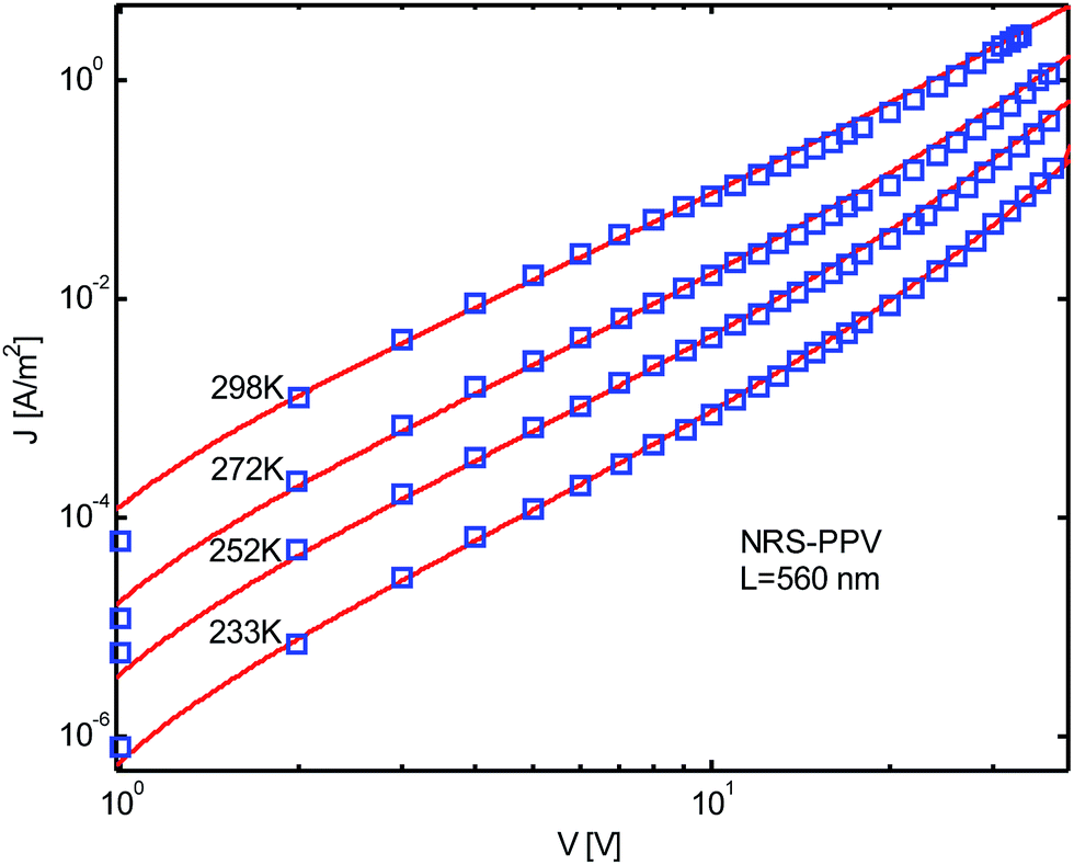 | ||
| Fig. 5 Experimental (symbols)8,10 and theoretical (lines) J–V curves of a NRS-PPV hole only diode, with thickness L = 560 nm and at different temperatures. | ||
 | ||
| Fig. 6 Experimental (symbols)8,10 and theoretical (lines) J–V curves of a OC1C10-PPV hole only diode, with thickness L = 275 nm and at different temperatures. | ||
 | ||
| Fig. 7 Experimental (symbols)5,42 and theoretical (lines) J–V curves of a P3HT hole only diode, with thickness L = 95 nm and at different temperatures. | ||
Nicolai et al.20,21 extracted parameters for the three materials as follows, σ ∼ 0.1 eV, Nt ∼ (1.3 × 10²³ to 4.0 × 10²³) m−3, (Et − Ev) ∼ 0.6 eV. Although they do not analyze variation of parameters with temperature, they postulate that the electron traps have a common origin, which is most likely related to hydrated oxygen complexes. However, analysis of the variation of parameters with temperature is very important to test the internal consistency of a theoretical model. Therefore, we list all parameters optimized in Tables 1 and 2. Our modified model yields σ ∼ (0.055–0.15) eV, Nt ∼ (7.5 × 10²² to 7.6 × 1024) m−3, (EtF = Et − EF) ∼ 0.2 eV. The dispersion of Nt is not in line with the postulation of Nicolai et al.20,21 The positive value of EtF means that the position of traps is higher than the Fermi energy EF. Table 1 also shows that the values of Wleft and Wright are non-symmetric, with Wright > Wleft and the built-in potential Vbi = Wright − Wleft in the devices is positive.
| NRS | OCC | P3HT | |
|---|---|---|---|
| σt (eV) | 0.055 | 0.1285 | 0.15 |
| Nt (m−3) | 7.55 × 10²² | 1.3 × 1024 | 1.7 × 1026 |
| EtF (eV) | 0.2 | 0.11 | 0.215 |
| Wleft (eV) | 0.1 | 0.375 | 0.35 |
| Wright (eV) | 1.01 | 0.578 | 0.69 |
| NRS | T (K) | 233 | 252 | 272 | 298 | |
| Nf (m−3) | 2.12 × 1025 | 2.2 × 1025 | 2.3 × 1025 | 2.4 × 1025 | ||
| μ0 (m2 V−1 s−1) | 1.4 × 10⁻¹¹ | 2.75 × 10⁻¹¹ | 3.9 × 10⁻¹¹ | 8.5 × 10⁻¹¹ | ||
| OCC | T (K) | 235 | 255 | 275 | 293 | |
| Nf (m−3) | 2.7 × 1026 | 2.8 × 1026 | 3.0 × 1026 | 3.5 × 1026 | ||
| μ0 (m2 V−1 s−1) | 1.1 × 10⁻⁷ | 1.2 × 10⁻⁷ | 1.4 × 10⁻⁷ | 1.5 × 10⁻⁷ | ||
| P3HT | T (K) | 215 | 235 | 255 | 275 | 294 |
| Nf (m−3) | 2.42 × 1033 | 1.36 × 1032 | 1.57 × 1031 | 3.07 × 1030 | 9.17 × 1029 | |
| μ0 (m2 V−1 s−1) | 8.35 × 10⁻⁵ | 1.7 × 10⁻⁴ | 3.23 × 10⁻⁴ | 3.75 × 10⁻⁴ | 4.25 × 10⁻⁴ |
We may further analyze variations of Nf and μ0 with temperature. We can fit Nf by using eqn (8) and determine the characteristic energies of EvF = Ev − EF and σ. The μ0 can be fitted by using the following non-Arrhenius expression.
| μ0 = μ00 exp[Δ/kT + λ(Δ/kT)2] | (31) |
 | ||
| Fig. 8 Variations of Nf(T) and μ0(T) with temperature. Symbols plot data listed in Table 2, and lines are the smoothed curves obtained by using eqn (9) and (31), respectively. | ||
| NRS | OCC | P3HT | |
|---|---|---|---|
| N0 (m−3) | 4.6756 × 1025 | 8.5742 × 1029 | 3.3709 × 1028 |
| EvF (eV) | −0.0214 | −0.3350 | −0.2524 |
| σ (eV) | 0.0149 | 0.0834 | 0.1305 |
| μ00 (m2 V−1 s−1) | 2.2073 × 10⁻⁶ | 2.6554 × 10⁻⁶ | 5.755 × 10⁻⁸ |
| Δ (eV) | −0.3411 | −0.1037 | 0.4744 |
| λ | 0.0175 | 0.0737 | −0.0279 |
5. Conclusion
In this work, we have analyzed variations of the density of trapped carriers with the density of free carriers, the effective mobility and the ratio of diffusion coefficient to effective mobility with the density of trapped carriers. It is shown that the density of trapped carriers is a dramatically increasing function of the density of free carriers at low density, and tends to saturation at high density. The density of trapped carriers is always an increasing function of the density of trapped carriers, and the slope dramatically increases at high density of trapped carriers. Although the ratio of diffusion coefficient to effective mobility is the Einstein type for free carriers, the ratio for total carriers is the non-Einstein type, and is an increasing function of the density of trapped carriers at low density, and a decreasing function at high density. This explains the recent argument about Einstein or non-Einstein types.We emphasize the importance of non-symmetric barriers at contacts to quantitatively describe the current–voltage relationships of typical organic layers sandwiched in two metallic electrodes. It is shown that slopes of current–voltage curves at low bias are very sensitive to the values of right barriers. The slopes in all bias are sensitive to the values of left barriers, and increase as the left barrier decreases.
When applying the modified model to three typical devices with organic NRS-PPV, OCC-PPV and P3HT layers, we obtain excellent agreement between theoretical results and experimental data. Evident improvement can be seen with our model when compared with the qualitative agreement of Nicolai et al.20,21 The extracted main parameters of materials are within the error range of Nicolai et al., and support the assumption that the electron traps have a common origin.
Acknowledgements
This work was supported by the Program for Excellent Talents of Sichuan Province of China under Grant no. 2011JQ0053, and the Science and Technology Foundation of State Key Laboratory for Shock Wave and Detonation Physics under Grant no. 9140C670103120C6702.References
- P. S. Davids, I. H. Campbell and D. L. Smith, Device model for single carrier organic diodes, J. Appl. Phys., 1997, 82, 6319 CrossRef CAS PubMed.
- B. K. Crone, P. S. Davids, I. H. Campbell and D. L. Smith, Device model investigation of bilayer organic light emitting diodes, J. Appl. Phys., 2000, 87, 19742 CrossRef PubMed.
- L. J. A. Koster, E. C. P. Smits, V. D. Mihailetchi and P. W. M. Blom, Device model for the operation of polymer/fullerene bulk heterojunction solar cells, Phys. Rev. B: Condens. Matter Mater. Phys., 2005, 72, 085205 CrossRef.
- M. C. J. M. Vissenberg and M. Matters, Theory of the field-effect mobility in amorphous organic transistors, Phys. Rev. B: Condens. Matter Mater. Phys., 1998, 57, 12964 CrossRef CAS.
- C. Tanase, E. J. Meijer, P. W. M. Blom and D. M. de Leeuw, Unification of the hole transport in polymeric field-effect transistors and light-emitting diodes, Phys. Rev. Lett., 2003, 91, 216601 CrossRef CAS.
- M. Kiguchi, M. Nakayama, T. Shimada and K. Saiki, Electric-field-induced charge injection or exhaustion in organic thin film transistor, Phys. Rev. B: Condens. Matter Mater. Phys., 2005, 71, 035332 CrossRef.
- F. Torricelli, K. O'Neill, G. H. Gelinck, K. Myny, J. Genoe and E. Cantatore, Charge transport in organic transistors accounting for a wide distribution of carrier energies – Part II: TFT modeling, IEEE Trans. Electron Devices, 2012, 59, 1520 CrossRef CAS.
- W. F. Pasveer, J. Cottaar, C. Tanase, R. Coehoorn, P. A. Bobbert, P. W. M. Blom, D. M. de Leeuw and M. A. J. Michels, Unified description of charge-carrier mobilities in disordered semiconducting polymers, Phys. Rev. Lett., 2005, 94, 206601 CrossRef CAS.
- J. Cottaar and P. A. Bobbert, Calculating charge-carrier mobilities in disordered semiconducting polymers: mean field and beyond, Phys. Rev. B: Condens. Matter Mater. Phys., 2006, 74, 115204 CrossRef.
- F. Torricelli, D. Zappa and L. Colalongo, Space-charge-limited current in organic light emitting diodes, Appl. Phys. Lett., 2010, 96, 113304 CrossRef PubMed.
- S. L. M. van Mensfoort and R. Coehoorn, Effect of Gaussian disorder on the voltage dependence of the current density in sandwich-type devices based on organic semiconductors, Phys. Rev. B: Condens. Matter Mater. Phys., 2008, 78, 085207 CrossRef.
- J. Li, J. X. Sun and C. Zhao, Improved expression of charge-carrier mobility in disordered semiconducting polymers considering dependence on temperature, electric field and charge-carrier density, Synth. Met., 2009, 159, 1915 CrossRef CAS PubMed.
- B. Xue, J. X. Sun and K. Yang, Improvement of unified mobility model with analytic current–voltage expression for organic diodes, J. Macromol. Sci., Part B: Phys., 2012, 51, 1415 CrossRef CAS.
- J. Zhou, Y. C. Zhou, J. M. Zhao, C. Q. Wu, X. M. Ding and X. Y. Hou, Carrier density dependence of mobility in organic solids: a Monte Carlo simulation, Phys. Rev. B: Condens. Matter Mater. Phys., 2007, 75, 153201 CrossRef.
- V. Coropceanu, J. Cornil, D. A. da Silva Filho, Y. Olivier, R. Silbey and J. L. Brédas, Charge transport in organic semiconductors, Chem. Rev., 2007, 107, 926 CrossRef CAS PubMed.
- R. Coehoorn and P. A. Bobbert, Effects of Gaussian disorder on charge carrier transport and recombination in organic semiconductors, Phys. Status Solidi A, 2012, 209, 2354 CrossRef CAS.
- H. Bässler and A. Köhler, Charge transport in organic semiconductors, Top. Curr. Chem., 2012, 312, 1 CrossRef.
- J. D. Myers and J. G. Xue, Organic semiconductors and their applications in photovoltaic devices, Polym. Rev., 2012, 52, 1 CrossRef CAS.
- Y. Zhang, B. de Boer and P. W. M. Blom, Trap-free electron transport in poly(p-phenylene vinylene) by deactivation of traps with n-type doping, Phys. Rev. B: Condens. Matter Mater. Phys., 2010, 81, 085201 CrossRef.
- H. T. Nicolai, M. M. Mandoc and P. W. M. Blom, Electron traps in semiconducting polymers: exponential versus Gaussian trap distribution, Phys. Rev. B: Condens. Matter Mater. Phys., 2011, 83, 195204 CrossRef.
- H. T. Nicolai, M. Kuik, G. A. H. Wetzelaer, B. de Boer, C. Campbell, C. Risko, J. L. Brédas and P. W. M. Blom, Unification of trap-limited electron transport in semiconducting polymers, Nat. Mater., 2012, 11, 882 CrossRef CAS PubMed.
- I. Lange, J. C. Blakesley, J. Frisch, A. Vollmer, N. Koch and D. Neher, Band bending in conjugated polymer layers, Phys. Rev. Lett., 2011, 106, 216402 CrossRef.
- J. Cottaar, L. J. A. Koster, R. Coehoorn and P. A. Bobbert, Scaling theory for percolative charge transport in disordered molecular semiconductors, Phys. Rev. Lett., 2012, 107, 136601 CrossRef.
- J. Cottaar, R. Coehoorn and P. A. Bobbert, Scaling theory for percolative charge transport in molecular semiconductors: correlated versus uncorrelated energetic disorder, Phys. Rev. B: Condens. Matter Mater. Phys., 2012, 85, 245205 CrossRef.
- J. O. Oelerich, D. Huemmer and S. D. Baranovskii, How to find out the density of states in disordered organic semiconductors, Phys. Rev. Lett., 2012, 108, 226403 CrossRef CAS.
- I. I. Fishchuk, A. Kadashchuk, S. T. Hoffmann, S. Athanasopoulos, J. Genoe, H. Bässler and A. Köhler, Unified description for hopping transport in organic semiconductors including both energetic disorder and polaronic contributions, Phys. Rev. B: Condens. Matter Mater. Phys., 2013, 88, 125202 CrossRef.
- P. de Bruyn, A. H. P. van Rest, G. A. H. Wetzelaer, D. M. de Leeuw and P. W. M. Blom, Diffusion-limited current in organic metal–insulator–metal diodes, Phys. Rev. Lett., 2013, 111, 186801 CrossRef CAS.
- L. W. Chen, R. Ludeke, X. D. Cui, A. G. Schrott, C. R. Kagan and L. E. Brus, Electrostatic field and partial Fermi level pinning at the Pentacene–SiO2 interface, J. Phys. Chem. B, 2005, 109, 1834 CrossRef CAS PubMed.
- S. Yogev, R. Matsubara, M. Nakamura, U. Zschieschang, H. Klauk and Y. Rosenwaks, Fermi level pinning by gap states in organic semiconductors, Phys. Rev. Lett., 2013, 110, 036803 CrossRef CAS.
- M. Oehzelt, N. Koch and G. Heimel, Organic semiconductor density of states controls the energy level alignment at electrode interfaces, Nat. Commun., 2014, 5, 4174 CAS.
- F. Neumann, Y. A. Genenko, C. Melzer and H. von Seggern, Self-consistent theory of unipolar charge-carrier injection in metal/insulator/metal systems, J. Appl. Phys., 2006, 100, 084511 CrossRef PubMed.
- F. Neumann, Y. A. Genenko, C. Melzer, S. V. Yampolskii and H. von Seggern, Self-consistent analytical solution of a problem of charge-carrier injection at a conductor/insulator interface, Phys. Rev. B: Condens. Matter Mater. Phys., 2007, 75, 205322 CrossRef.
- Y. Roichman and N. Tessler, Generalized Einstein relation for disordered semiconductors—implications for device performance, Appl. Phys. Lett., 2002, 80, 1948 CrossRef CAS PubMed.
- Y. Q. Peng, J. H. Yang and F. P. Lu, et al. Einstein relation in chemically doped organic semiconductors, Appl. Phys. A: Mater. Sci. Process., 2007, 86, 225 CrossRef CAS.
- A. Das and A. Khan, Mobility–diffusivity relationship for heavily doped organic semiconductors, Appl. Phys. A: Mater. Sci. Process., 2008, 93, 527 CrossRef CAS.
- X. H. Lu, J. X. Sun, Y. Guo and D. Zhang, Potential-dependent generalized Einstein relation in disordered organic semiconductors, Chin. Phys. Lett., 2009, 26, 087202 CrossRef.
- F. Neumann, Y. A. Genenko and H. von Seggern, The Einstein relation in systems with trap-controlled transport, J. Appl. Phys., 2006, 99, 013704 CrossRef PubMed.
- G. A. H. Wetzelaer, L. J. A. Koster and P. W. M. Blom, Validity of the Einstein relation in disordered organic semiconductors, Phys. Rev. Lett., 2011, 107, 066605 CrossRef CAS.
- H. K. Gummel, A self-consistent iterative scheme for one-dimensional steady state transistor calculations, IEEE Trans. Electron Devices, 1964, 11, 455 CrossRef PubMed.
- D. L. Scharfetter and H. K. Gummel, Large-signal analysis of a silicon read diode oscillator, IEEE Trans. Electron Devices, 1969, 16, 64 CrossRef PubMed.
- G. Paasch and S. Scheinert, Charge carrier density of organics with Gaussian density of states: analytical approximation for the Gauss–Fermi integral, J. Appl. Phys., 2010, 107, 104501 CrossRef PubMed.
- N. I. Craciun, J. Wildeman and P. W. M. Blom, Universal Arrhenius temperature activated charge transport in diodes from disordered organic semiconductors, Phys. Rev. Lett., 2008, 100, 056601 CrossRef CAS.
| This journal is © The Royal Society of Chemistry 2015 |