Synthesis of single-crystalline NdB6 submicroawls via a simple flux-controlled self-catalyzed method†
Wei Hana,
Hao Zhangb,
Jian Chen*b,
Yanming Zhao*a,
Qinghua Fana and
Qidong Lia
aState Key Laboratory of Luminescent Materials and Devices, South China University of Technology, Guangzhou, 510641, P. R. China. E-mail: zhaoym@scut.edu.cn
bInstrumental Analysis and Research Centre, Sun Yat-Sen University, Guangzhou, 510275, P. R. China. E-mail: puscj@mail.sysu.edu.cn
First published on 5th January 2015
Abstract
Neodymium hexaboride (NdB6) submicroawls have been fabricated via a simple flux-controlled self-catalyzed method using neodymium (Nd) powders and boron trichloride (BCl3) as starting materials at 1000 °C. Scanning electron microscopy (SEM) reveals that the submicroawls are tapered, with a length of 2–5 μm and a diameter ranging from approximately 0.1–0.3 μm at the roots and 5–50 nm at the tips. Transmission electron microscopy (TEM) shows that the submicroawls are single crystalline with the preferred growth direction along [001]. For systematic research, we have discussed the morphological change of NdB6 submicron structures by varying reaction temperatures, catalysts and duration. Moreover, a multistage growth model of the NdB6 submicroawls is proposed.
I. Introduction
One-dimensional (1D) rare-earth hexaboride (RB6) nanostructures have been considered as the most promising candidates with excellent properties for field emitters, not only because of their outstanding mechanical properties, high melting points, low volatility at high temperature, high brightness and high chemical stabilities but also due to their high aspect ratio and relatively low work function.1–3 It is known that materials with anisotropic structures and sharp tips or edges can greatly increase the emission current. Anisotropic nanostructures are better field emitters4,5 where the emission current is strongly dependent upon the work function of the emitter surface, the radius of curvature of the emitter apex and the emission area.6,7 The Fowler–Nordheim (F–N) theory4 predicts that electron emitters made of materials with a low work function, higher aspect ratio and higher curvature of the tips, could greatly enhance the field emission (FE) current with a lower applied turn-on voltage.As one of the rare earth hexaboride family members, neodymium hexaboride (NdB6) has been reported to have a lower work function (1.6 eV)8 than many previously reported cathode materials, including RB6 (LaB6 ∼ 2.7 eV;9 CeB6 ∼ 2.5 eV (ref. 10)), ZnO (5.3 eV)11 and widely used tungsten (4.6 eV).12 If single-crystalline NdB6 nanostructures with high aspect ratio morphology, such as nanowires or nanotubes, can be fabricated, it may be an ideal candidate for the investigation and development of advanced field emission theory, and efficient cathodes for vacuum electronic devices. Recently, Wang developed a palladium-nanoparticle-catalyzed chemical vapor deposition (CVD) method to synthesize NdB6 nanoobelisks and nanowires,13 but the boron precursor (B10H14) was toxic and the Pd–Nd–B alloy drops on the tips would limit the electron emission and reduce the current density.14 Very recently, Xu et al. reported the synthesis of NdB6 nanowires and nanoneedles via a catalyst-free CVD approach.15 However, the boron source they used was highly poisonous and combustible diborane (B2H6), which required more stringent safety methods for storage and waste disposal. Therefore, a more effective and safer method to synthesize NdB6 nanostructures should be developed.
In this paper, we report the synthesis of the NdB6 submicroawls via a simple flux-controlled self-catalyzed method.16–18 Scanning electron microscopy (SEM) reveals that the submicroawls are tapered, with a length of 3–5 μm and a diameter ranging from approximately 0.1–0.3 μm at the roots and 5–50 nm at the tips. Transmission electron microscopy (TEM) shows that the submicroawls are single crystalline with the preferred growth direction along [001]. Moreover, we have discussed the morphological change of NdB6 submicron structures at different reaction temperatures, catalysts and duration time. In addition, a multistage growth model of the NdB6 submicroawls is proposed.
II. Experimental section
The NdB6 awl-like submicrostructures were prepared by a self-catalyzed scheme16 via a simple flux-controlled method with neodymium and boron trichloride as the source materials. The synthesis was based on the following chemical reaction: Nd(s) + 6BCl3(g) + 9H2(g) = NdB6(s) + 18HCl(g). The synthesis was performed in a horizontal high-temperature tube furnace (Shenjia Kiln, Luoyang, China). The real temperature in the flat-temperature zone was measured by a thermocouple which was mounted at the center of the tube. The silicon ((100) plane, Empak, USA) substrates (8 × 8 mm2) were used for the experiments. They were ultrasonically cleaned using distilled water and ethanol. The Si substrates were then loaded inside a quartz boat. Precursor Nd metal powders (weight 0.5 mg, purity 99.9%, particle size less than 96 μm, Institute of Rare Earths, Baotou, China) were well deposited on the Si substrates. The quartz boat was then quickly placed into the flat-temperature zone of the horizontal tube furnace, and the furnace tube was purged with high-purity gas mixture (50% H2 + 50% Ar, 99.99%, Ruimin Gas, Guangzhou, China) for 2 h before heating to eliminate any oxygen in the furnace. The tube temperature was heated to 1000–1100 °C at 10 °C min−1 with a 50 sccm (standard cubic centimeters per minute) continuous flow of gas mixture (50% H2 + 50% Ar) and kept at this temperature for 50 min. When the tube reached the desired temperature, a steady BCl3 (99.99%, Summit Specialty Gases, Tianjin, China) flow of 20 sccm was introduced to the tube for 30–40 min and then the BCl3 flow was switched off in order to reduce the flux of B (active boron). After the reaction, the tube was cooled down to room temperature in 5 h under the 50% H2 + 50% Ar mixed gas atmosphere. All the experiments were carried out at 1 atm. Then the products were washed with diluted hydrochloric acid and distilled water for several times to remove the potential impurities (Nd2O3, H3BO3). After drying at 60 °C for 1 h, the final gray products were obtained. Four representative samples with different morphologies (submicroawl, submicrotube, submicrowire and submicrorod) were fabricated by varying some experimental parameters, and the detailed growth conditions are presented in the following context.The products were characterized and analyzed by X-ray diffraction (XRD, TD-3500), field emission scanning electron microscopy (FE-SEM, Navo NanoSEM430), high resolution transmission electron microscopy (HRTEM, JEM-2010HR) installed with energy dispersive X-ray spectroscopy (EDX, Oxford), and selected area electron diffraction (SAED, JEM-2010HR).
III. Results
The phase identification of the product was carried out using X-ray powder diffraction. Shown in Fig. 1 are the X-ray diffraction (XRD) patterns of the obtained NdB6 submicron structures at various temperatures with catalyst-free: (a) 1000 °C; (b) 1050 °C; (c) 1100 °C and the standard NdB6 powder diffraction pattern from the Inorganic Crystal Structure Database (ICSD, no. 108069) (bottom curve). No characteristic peaks of impurities are detected, indicating the purity of the products. All the diffraction peaks can be indexed by using Dicvol program and assigned to the lattice planes of (100), (110), (111), (200), (210), (211), (220) for the corresponding “d” spacing. The calculated lattice parameters of cubic NdB6 obtained in 1000 °C, 1050 °C and 1100 °C are 0.412(2) nm, 0.412(6) nm and 0.412(8) nm, respectively. The results agree with the standard NdB6 powder diffraction lattice parameters of a = 0.412(8) nm and a space group of Pm![[3 with combining macron]](https://www.rsc.org/images/entities/char_0033_0304.gif) m.
m.
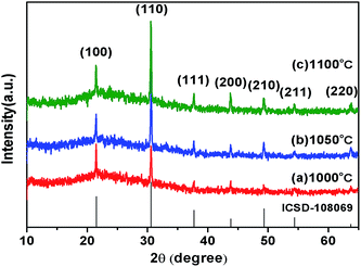 | ||
| Fig. 1 XRD patterns of the as-synthesized NdB6 submicron structures at various temperatures: (a) 1000 °C; (b) 1050 °C; (c) 1100 °C. | ||
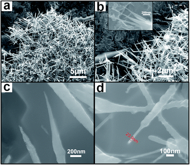
Fig. 2 shows the typical SEM images of the NdB6 submicroawls obtained on the Si substrates at 1000 °C with a reaction time of 50 min where the duration time of a flow of BCl3 (20 sccm) is 40 min. The low-magnification image of Fig. 2a reveals that the final product is composed of submicroawls in a uniform morphology. The submicroawls are straight and about 2–5 μm in length. Fig. 2b shows most of the submicroawls are tapered. Fig. 2b inset is a higher-magnification image, showing that the awl-handles have an average diameter of 0.15 μm, and the awl tips have a diameter in a range of 5–50 nm. Due to the handle-to-tip diameter ratios of 3 to 30, we call them submicroawls. As demonstrated in Fig. 2c and d, the products can be classified into two types of awl-like morphology according to their tips. The tip of the submicroawl in Fig. 2c is extremely sharp and tapered, while the tip of the submicroawl in Fig. 2d is very straight and the entire submicroawl is just like a screwdriver. Obviously, these submicroawls possessing extremely sharp tips are very important and beneficial for field-induced electron emission. It is noticeable that no catalytic particles can be observed at the tips of the submicroawls. Due to the absence of silicon-containing nanoparticles or other metal catalysts in our products, we conclude that the growth of submicroawls occurred directly on the Nd metal which acted as neodymium source and catalyst contemporaneously. In other words, the growth process of the submicroawls is attributed to the self-catalyzed mechanism.
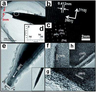
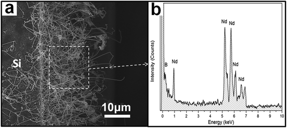
The detailed information regarding the crystallinity, morphology, chemical composition, and growth direction of the NdB6 submicroawls were further characterized by transmission electron microscopy (TEM).19 Fig. 3 illustrates typical zoom-in TEM images of two single NdB6 submicroawls. Fig. 3a shows that the submicroawl is tapered from bottom to top and it has an ultra-sharp tip with a diameter of about 5 nm. Moreover, no obvious particles can be observed from the tip of the submicroawl, which implies that no extra catalyst is involved during the synthesis process. Fig. 3b reveals that this submicroawl is grown in the preferred [001] crystallographic direction of the cubic NdB6 with lattice parameter of a = 0.412(3) nm. The selected area electron diffraction (SAED) image (Fig. 3c) along the [![[1 with combining macron]](https://www.rsc.org/images/entities/char_0031_0304.gif) 10] crystal zone axis shows regular diffraction spots such as (110), (001) and (111) planes. The diffraction pattern appears identical as we moved the SAED aperture along the entire submicroawl, suggesting that the NdB6 submicroawl is single crystalline. The EDX (Fig. 3d) indicates that the submicroawl consists of Nd and B compositions with the molar ratio ∼1
10] crystal zone axis shows regular diffraction spots such as (110), (001) and (111) planes. The diffraction pattern appears identical as we moved the SAED aperture along the entire submicroawl, suggesting that the NdB6 submicroawl is single crystalline. The EDX (Fig. 3d) indicates that the submicroawl consists of Nd and B compositions with the molar ratio ∼1![[thin space (1/6-em)]](https://www.rsc.org/images/entities/char_2009.gif) :
:![[thin space (1/6-em)]](https://www.rsc.org/images/entities/char_2009.gif) 6 and no other impurity can be found. In order to explore the growth mechanism of the NdB6 submicroawls, the detailed atomic structure around the tip of another submicroawl (see the inset of Fig. 3e) has been analyzed. Fig. 3e shows that the tip of the NdB6 submicroawl is ladder-shaped, and it is terminated by several different lattice planes that are marked with letters F to H on the image. The corresponding HRTEM images are showed in Fig. 3f–h.
6 and no other impurity can be found. In order to explore the growth mechanism of the NdB6 submicroawls, the detailed atomic structure around the tip of another submicroawl (see the inset of Fig. 3e) has been analyzed. Fig. 3e shows that the tip of the NdB6 submicroawl is ladder-shaped, and it is terminated by several different lattice planes that are marked with letters F to H on the image. The corresponding HRTEM images are showed in Fig. 3f–h.
Fig. 3f shows the lateral lattice of the tip marked with letter F in Fig. 3e, which is terminated with the (111) lattice plane. Fig. 3g shows a (001) facet, which is perpendicular to the submicroawl axis [001]. The [001] growth of these NdB6 submicroawls is attributed to the fact that the {001} lattice planes of NdB6 have the highest atomic density, and therefore, it would minimize the total energy for the crystal to grow in this lattice direction.2 Fig. 3h shows (1![[1 with combining macron]](https://www.rsc.org/images/entities/char_0031_0304.gif) 1) facet corresponding to the area marked with H in Fig. 3e. The above results indicate that the {001}, {111} and {1
1) facet corresponding to the area marked with H in Fig. 3e. The above results indicate that the {001}, {111} and {1![[1 with combining macron]](https://www.rsc.org/images/entities/char_0031_0304.gif) 1} type planes with low indices are the dominant terminating lattice planes which agree with the lowest energy principle in crystal growth. Moreover, it is reasonable that the growth rate of lateral lattices (111) and (1
1} type planes with low indices are the dominant terminating lattice planes which agree with the lowest energy principle in crystal growth. Moreover, it is reasonable that the growth rate of lateral lattices (111) and (1![[1 with combining macron]](https://www.rsc.org/images/entities/char_0031_0304.gif) 1) is slowing down during the last stage, because the tip is grown at the last stage when the flux concentration of BCl3 is decreasing. This result will give rise to the reduction in the ratio of lateral vs. vertical growth, leading to the tapered structures.
1) is slowing down during the last stage, because the tip is grown at the last stage when the flux concentration of BCl3 is decreasing. This result will give rise to the reduction in the ratio of lateral vs. vertical growth, leading to the tapered structures.
IV. Discussion
To explore the growth mechanism of as-synthesized NdB6 submicroawls, a series of systematic experiments were carried out to study the effects of reaction temperatures, catalytic materials and reaction duration. A “self-catalyzed” growth mechanism was proposed based on the experimental results.1. Effect of reaction temperatures
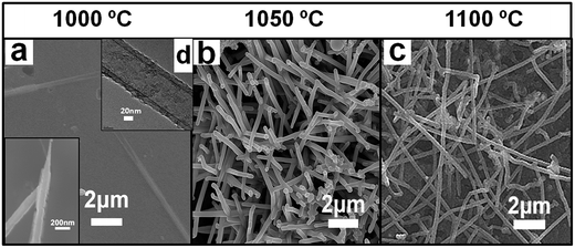
The morphological structures of NdB6 Submicron materials were found to be strongly influenced by the reaction temperatures to yield different 1D submicron structures – submicroawls, submicrotubes, submicrorods and submicrowires. With other parameters (i.e., reaction duration, flow rate and flow duration time, heating and cooling rate, catalyst-free, etc.) unchanged, the reaction temperatures were varied from 1000 °C to 1100 °C. XRD patterns of the as-synthesized NdB6 submicron structures at various temperatures are shown in Fig. 1. Typically, at a low reaction temperature (1000 °C), straight tapered submicroawls with length ranging from about 2–5 μm are obtained (Fig. 2, 3 and 4a inset). Besides, at this lower temperature (compared to the melting point 1024 °C of metal neodymium) the NdB6 submicrotubes with very small amount are also found on the substrate but in the different locations (Fig. 4a). As it can be seen from Fig. 4a, there are two NdB6 submicrotubes which have diameters of 0.2–0.3 μm and lengths of 10–20 μm. In order to clearly recognize and confirm the tubular structure, the TEM image has been presented in Fig. 4d where a hollow interior channel structure comes into view. As to the formation of tubular structures under a self-catalyzed mechanism, the related reports are few. A broad accepted growth model is proposed by Erick et al. who considered that the formation of hollow nanotubes can be ascribed to the diffusion limit in the droplet at high temperature, which results in the ring-shaped nucleation and induced the growth of nanotubes.20 In this work, the growth mechanism of NdB6 tubes is similar to the formation model of PrB6 nanotubes.21At a reaction temperature of 1050 °C, the NdB6 submicron structures undergo a morphology transition from submicroawls/tubes to rods without tapered tips (Fig. 4b). SEM images show that the average diameters and lengths of these rods are 0.15–0.3 μm and 2–8 μm. At the highest temperature (1100 °C), NdB6 submicrowires are grown instead (Fig. 4c). The average length of ∼20 μm of the submicrowires is larger than that of the submicroawls grown at 1000 °C and the submicrorods grown at 1050 °C. These results are principally attributed to the enhancement of growth rates with the increasing temperature. Note that the submicroawls and submicrotubes can be only fabricated at 1000 °C, so we infer that the reaction temperature may be the key factor for the growth of the two morphologies.
2. Effect of catalytic materials
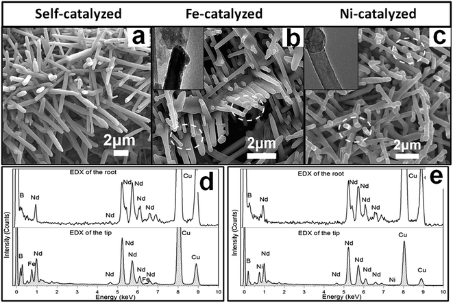
To probe the effect of catalysts on NdB6 products, we compared self-catalyzed growth (SCG) and metal-catalyzed growth (MCG) (M = Fe, Ni) at 1050 °C. Here, the metal Fe/Ni was obtained from the high temperature reduction of Fe(NO3)3/Ni(NO3)2 by H2. The Fe(NO3)3/Ni(NO3)2 film was coated on the Si substrates by a drop-casting method. 1D submicron structures can be identified from the substrates after both SCG and MCG. However, the morphologies of samples through these two methods are different. Typically, in a SCG method, long submicrorods with length ranging from about 2–8 μm are obtained (Fig. 5a and 4b). The diameter of these rods is about 150 nm to 300 nm. While using MCG method, we can obtain short straight rods with branches (Fig. 5b and c). The diameter of these rods is about 50 nm to 200 nm. The average length of ∼3 μm of the rods in the sample is much shorter than the rods grown by the SCG method. Moreover, a small globule is present at the tip of the rod by the MCG method (circled in Fig. 5b and c), while no globule can be observed at the tip of the rod by the SCG method (Fig. 5a). In order to confirm the existing of catalysts at the tips of those submicron structures, the TEM images are presented in the insets of Fig. 5b and c, where the small globules can be visible. Furthermore, the EDX was used to show the compositions at the tips of the as-synthesized submicrostructures. Fig. 5d and e and 3d show the compositions of the as-synthesized submicrostructures with and without using catalysts during synthesis process. In Fig. 5d and e, the signals of Fe and Ni are present in the EDX of the tips, and this result shows the catalytic materials are included in the tips. These results are maybe owing to the different growth mechanisms of these two methods. Hence, we hypothesize that the MCG method is dominated by a nontraditional VLS (vapor–liquid–solid) growth mechanism. Although detailed information on the ternary phase diagram of Nd–B–M is not available, small miscible Nd–B–M liquid alloy droplets may be formed and act as nucleation sites. The continuous supply of boron causes the liquid Nd–B–M droplets to become supersaturation, resulting in the precipitation of NdB6 as rods by the VLS-like growth mechanism. Because of this process, the globules on the tips appears which is just similar to the Au-catalytic Si whisker growth and Sn-guided ZnO 1D nanostructure growth.22,23 However, there are no globules found in the SCG method owing to the different mechanism in the following discussion. In addition to Fe and Ni, other catalytic material such as platinum (Pt) was employed in experiments (not shown here). Fe was found to have the highest catalytic efficiency, followed by Ni and Pt. Furthermore, the compositions at the roots were also studied (Fig. 5d and e) and compared to those at the tips. No signals of Fe and Ni observed at the root of the as-synthesized structures suggests that these structures are grown by the tip-based VLS mechanism.3. Effect of reaction duration
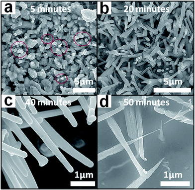
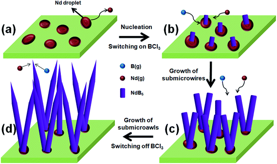
A time trial growth study was conducted for further insight into the catalyst-free growth of the submicroawls at 1000 °C. Here, the reaction duration was adopted as 5 min, 20 min, 40 min and 50 min and the corresponding duration time of a flow of BCl3 (20 sccm) was 5 min, 20 min, 40 min and 40 min, respectively. The time-dependent morphological evolution of NdB6 submicroawls is shown in Fig. 6. Initially, for submicron structures grown with a shorter reaction time (5 min), a thin layer of cubic-shaped film of NdB6 was deposited on the silicon substrate. Moreover, some short rods (marked by the circles in (a)) can be identified (Fig. 6a). As discussed later in the text, it is believed that the film and short rods are the nucleation and initial growth of NdB6 which plays an important role for further growth of NdB6 1D submicron structures. For submicron structures grown with an intermediate reaction time (20 min), thicker and longer 1D submicron structures are obtained as shown in Fig. 6b. In this period, the observed increase in the heights and widths of the materials suggests the growth process followed a continuous self-catalyzed vertical growth with lateral growth. During the 40 min growth period, the tips of the wires are not tapered (Fig. 6c). However, the evolution of these wires into awl structures occurred between the 40–50 min reaction period after the BCl3 gas was switched off (Fig. 6d). As BCl3 precursor flux was very important for the growth of 1D submicron structures, so it could be assumed that the BCl3 flux was a key factor for the formation of submicroawls. Once the BCl3 precursor was switched off, the local concentration at the growth zone decreased until the remaining BCl3 flow was completely exhausted. This decrease in concentration gradient was expected to cause a decrease in the ratio of lateral vs. vertical growth, leading to the growth of tapered tops of the submicroawls. In short, time-dependent morphological evolution of NdB6 1D submicron structures was revealed, and the results are beneficial for the further understanding of possible growth mechanism of the submicroawls.4. Growth mechanism
SEM and TEM analysis show that the growth of the submicroawls may not be governed by the conventional VLS process proposed that the nanowires grew by the catalytic-assisted approach, in which a metal particle is located at the growth front of the wire and acts as the catalytic active site. Moreover, no catalytic particles are found on the tips of the submicroawls, and it is likely that the growth is dominated by a “self-catalyzed” mechanism.16–18,21 In this work, melting metal Nd plays the roles of both raw material and catalyst simultaneously in the process of synthesizing NdB6 submicroawls. Four main steps involved in the growth for the submicroawls are outlined as following (Fig. 7a–d).V. Conclusion
In summary, single-crystalline NdB6 submicroawls were achieved via a simple flux-controlled self-catalyzed method. The tapered submicroawls had a length of 2–5 μm and a diameter ranging from approximately 0.1–0.3 μm at the roots and 5–50 nm at the tips. Our results suggest that Nd liquid droplets and Nd vapor can coexist as the source for the growth of NdB6 1D submicron structures although the reaction temperature of 1000 °C is lower than the Nd melting point of 1024 °C. Furthermore, a concentration gradient is necessary to create these awl-like structures where the combination of SC and VS growth is responsible for the growth of tapered NdB6 submicroawls. Due to the poor conductivity of the Si substrates which resulted from the eroding by the BCl3 gas to form the rough background,16 the work on the field emission is difficult to conduct using the as-synthesized product. Further studies to reveal the effect of geometry for single submicroawls on their field-emission properties will be performed in the future. We expect that this work will arouse further interest and investigation of morphological control of submicrostructures and their properties.Acknowledgements
This work was funded by NSFC Grant (no. 51172077, 51372089, 51373205) supported through NSFC Committee of China, the Foundation of (no. S2011020000521) supported through the Science and Technology Bureau of Guangdong Government and the Foundation of (no. 2014ZB0014, 2013ZM0111) supported through the Fundamental Research Funds for the Central Universities.References
- H. Zhang, Q. Zhang, J. Tang and L. C. Qin, J. Am. Chem. Soc., 2005, 127, 2862 CrossRef CAS PubMed.
- H. Zhang, J. Tang, Q. Zhang, G. Zhao, G. Yang, J. Zhang, O. Zhou and L. C. Qin, Adv. Mater., 2006, 18, 87 CrossRef CAS.
- H. Zhang, J. Tang, J. Yuan, J. Ma, N. Shinya, K. Nakajima, H. Murakami, T. Ohkubo and L. C. Qin, Nano Lett., 2010, 10, 3539 CrossRef CAS PubMed.
- R. H. Fowler and L. Nordheim, Proc. R. Soc. London, 1928, 119, 173 CrossRef CAS.
- W. A. D. Heer, A. Chatelain and D. Ugarte, Science, 1995, 270, 1179 Search PubMed.
- L. Vila, P. I. Vincent, L. D. De Pra, G. Pirio, E. Minoux, L. Gangloff, S. Champagne, N. Sarazin, E. Ferain, R. Legras, L. Piraux and P. Legagneux, Nano Lett., 2004, 4, 521 CrossRef CAS.
- B. Varghese, T. C. Hoong, Z. Yanwu, M. V. Reddy, B. V. R. Chowdari, A. T. S. Wee, T. B. C. Vincent, C. T. Lim and C. H. Sow, Adv. Funct. Mater., 2007, 17, 1932 CrossRef CAS.
- P. H. Schmidt, L. D. Longinotti, D. C. Joy, S. D. Ferris, H. J. Leamy and Z. J. Fisk, Vac. Sci. Technol., 1978, 15, 1554 CrossRef CAS.
- A. Yutani, A. Kobayashi and A. Kinbara, Appl. Surf. Sci., 1993, 70, 737 CrossRef.
- P. R. Davis, M. A. Gesley, G. A. Schwind, L. W. Swanson and J. Hutta, Appl. Surf. Sci., 1989, 37, 381 CrossRef CAS.
- T. Minami, T. Miyata and T. Yamamoto, Surf. Coat. Technol., 1998, 108, 583 CrossRef.
- T. Kawakubo, Y. Shimoyama, H. Nakane and H. Adachi, J. Vac. Sci. Technol., B: Microelectron. Nanometer Struct.–Process., Meas., Phenom., 2008, 26, 1395 CrossRef CAS.
- G. Wang, J. R. Brewer, J. Y. Chan, D. R. Diercks and C. L. Cheung, J. Phys. Chem. C, 2009, 113, 10446 CAS.
- W. Zhu, G. P. Kochanski and S. Jin, Science, 1998, 282, 1471 CrossRef CAS.
- J. Xu, G. Hou, T. Mori, H. Li, Y. Wang, Y. Chang, Y. Luo, B. Yu, Y. Ma and T. Zhai, Adv. Funct. Mater., 2013, 23, 5038 CrossRef CAS.
- J. Xu, Y. Zhao and C. Zou, Chem. Phys. Lett., 2006, 423, 138 CrossRef CAS PubMed.
- Q. Ding, Y. Zhao, J. Xu and C. Zou, Solid State Commun., 2007, 141, 53 CrossRef CAS PubMed.
- Q. Fan, Q. Zhang, Y. Zhao and Q. Ding, J. Rare Earths, 2013, 31, 145 CrossRef CAS.
- Y. Ding and Z. L. Wang, J. Phys. Chem. B, 2004, 108, 12280 CrossRef CAS.
- E. P. A. M. Bakkers and M. A. Verheijen, J. Am. Chem. Soc., 2003, 125, 3440 CrossRef CAS PubMed.
- M. Chi, Y. Zhao, Q. Fan and W. Han, Ceram. Int., 2014, 40, 8921 CrossRef CAS PubMed.
- R. S. Wagner and W. C. Ellis, Appl. Phys. Lett., 1964, 4, 89 CrossRef CAS PubMed.
- Y. Ding, P. X. Gao and Z. L. Wang, J. Am. Chem. Soc., 2004, 126, 2066 CrossRef CAS PubMed.
- C. E. Habermann and A. H. Daane, J. Chem. Phys., 1964, 41, 2818 CrossRef CAS PubMed.
- Z. W. Pan, Z. R. Dai and Z. L. Wang, Science, 2001, 291, 1947 CrossRef CAS PubMed.
- J. R. Brewer, N. Deo, Y. M. Wang and C. L. Cheung, Chem. Mater., 2007, 19, 6379 CrossRef CAS.
- Z. Z. Yea, J. Y. Huang, W. Z. Xu, J. Zhou and Z. L. Wang, Solid State Commun., 2007, 141, 464 CrossRef PubMed.
- T. Zhai, Z. Gu, H. Fu, Y. Ma and J. Yao, Cryst. Growth Des., 2007, 7, 1388 CAS.
Footnote |
| † Electronic supplementary information (ESI) available. See DOI: 10.1039/c4ra13129k |
| This journal is © The Royal Society of Chemistry 2015 |

