DOI:
10.1039/C5RA03125G
(Paper)
RSC Adv., 2015,
5, 34730-34736
Spectra and energy levels of a layered Yb3+:CsGd(MoO4)2 crystal with perfect cleavage: a candidate for microchip lasers
Received
18th February 2015
, Accepted 9th April 2015
First published on 10th April 2015
Abstract
Thin mica-like Yb3+:CsGd(MoO4)2 crystals, with a perfect (100) cleavage plane, have been grown by a top seeded solution growth method from a flux of Cs2Mo3O10. The cleavage habit has been found to be closely connected with the layered structure. The Stark-level positions of Yb3+ have been deduced from the excitation and emission spectra at 77 K with the aid of the Raman spectrum, indicating the largest ground-state splitting among the double molybdates and double tungstates ever reported except for Yb3+:LiLu(WO4)2. The emission cross-sections have been determined by the combinatorial reciprocity method and the Füchtbauer–Ladenburg formula. The wavelength dependence of the gain cross-section predicts a broad tuning range and potential sub-100 fs laser pulse generation. Taking into account the cleavage behavior, the crystal is particularly suitable for microchip lasers, in which thin platelets of gain media can be prepared by a simple cleavage technique.
1. Introduction
Double molybdate (DMo) and double tungstate (DW) crystals with the general formula M+T3+(X6+O4)2 (X = Mo or W), have aroused considerable interest due to their outstanding performance as gain media for thin-disk, tunable, and ultrafast pulsed lasers or as nonlinear elements for laser Raman shifting.1–4 The majority of the DMo and DW crystals with M = Li and Na, have disordered tetragonal structure. Once doped with lasing ions (Yb3+, Tm3+, etc.), they exhibit low peak optical cross-sections and large inhomogeneously-broadened spectral bands owing to the structural disorder and multisite character of hosts.4–7 On the contrary, the ordered monoclinic DMo and DW crystals with M = K are characterized by the narrow bandwidths and the pronounced spectral anisotropy, resulting in high peak optical cross-sections in specific crystal orientations.4,8,9 In order to improve the laser performance especially for tunable and ultrafast (<100 fs) pulsed lasers, it is of great importance to explore new laser-active crystalline materials with intermediate bandwidths and optical cross-sections.
To our knowledge, the literatures on the DMo and DW crystals with M = Rb and Cs are still limited. Most likely, the difficulties (e.g., incongruent melting, structural transformation and cleavage) in the growth of single crystals with centimeter dimensions hamper the spectroscopic analysis and laser applications.10,11 Our group have presented the growth and spectroscopic characterization of Nd3+:CsLa(WO4)2 crystal,11 an interesting crystal with the ordered tetragonal structure. Unfortunately, we failed to obtain the nominal Yb3+:CsLa(WO4)2 crystal, since Yb3+ could hardly incorporate into the crystal lattice.
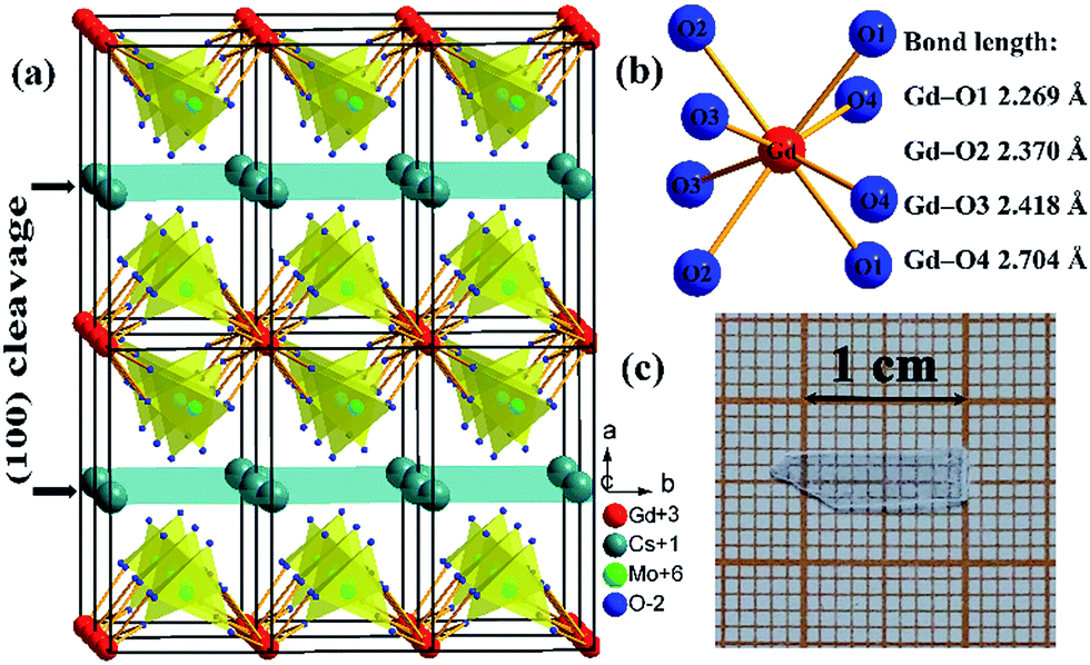
CsGd(MoO4)2 (CGM) crystallizes in the monoclinic system with the space group P2/c and the cell parameters: a = 9.5289(2) Å, b = 5.0823(2) Å, c = 8.0563(7) Å, β = 91.246(6)°, and Z = 2.12 The CGM features a highly anisotropic layered crystal structure (Fig. 1a), which gives rise to some interesting phenomena as a dipolar magnet.13 The Eu3+:CGM red-emitting phosphor is also reported to be attractive for potential applications in the white light-emitting diode devices.12 From the structural point of view, CGM offers a highly distorted cationic site suitable for lasing ions, especially for Yb3+. Yb3+ lasers operate in a quasi-three-level scheme, since the fundamental and terminal laser levels belong to the same 2F7/2 manifold. In order to limit the thermal population of the terminal level, the crystal-field splitting of the 2F7/2 manifold ΔE as large as possible is desirable. Considering the ΔE is sensitive to the crystal field, one important strategy to extend the ΔE is to employ hosts that accommodate Yb3+ with low site symmetry and different Yb–O distances.14 Similar to the famous KGd(WO4)2,15 Gd3+ occupies an eight-coordinated site (Wyckoff position: 2e) of CGM with C2 symmetry and Gd–O distances ranging from 2.269 Å to 2.704 Å (Fig. 1b). The distortion degree of the [GdO8] polyhedron in CGM is even greater than that in KGd(WO4)2 with the minimum Gd–O distance of 2.271 Å and maximum of 2.650 Å. Such a highly distorted local environment is expected to produce an intensive crystal-field strengths and thus large ΔE of Yb3+. Moreover, the absence of the structural disorder or multisite character in CGM predicts high optical cross-sections and moderate bandwidths. Based on the above consideration, we investigated the crystal growth and the spectroscopic characteristics of the Yb3+:CGM crystal so as to evaluate its feasibility for laser applications.
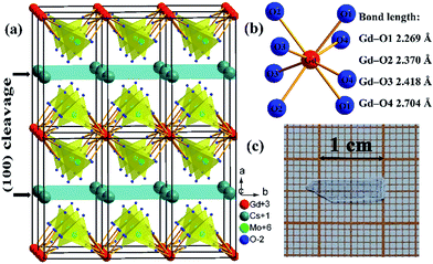 |
| | Fig. 1 The photographs of (a) crystal structure, (b) coordination environment of Gd3+ and (c) a typical (100) cleavage slice of the Yb3+:CGM crystal. | |
2. Experimental
2.1 Crystal growth
CGM was found to decompose into Gd2MoO6 in a peritectic reaction at 1035 °C.16 The incongruent-melting Yb3+:CGM crystals were elaborated by the top seeded solution growth (TSSG) technique. The growth was performed in a vertical tubular furnace equipped with a Ni–Cr wire and a temperature controller. Cs2Mo3O10 was chosen as a flux, since the self-flux do not introduce impurity. According to the solubility curve of the CGM-Cs2Mo3O10 system,16 the molar ratio of Yb3+:CGM to Cs2Mo3O10 was set as 1![[thin space (1/6-em)]](https://www.rsc.org/images/entities/char_2009.gif) :2, thereby ensuring appropriate saturation temperature (∼930 °C) for crystal growth. The starting materials including Cs2CO3 (A.R.), Gd2O3 (4N), Yb2O3 (4N) and MoO3 (A.R.), were weighed, mixed, transferred into a Pt crucible and heated up to 1000 °C for 10 h to homogenize the solution. At first the crystal were grown by spontaneous nucleation using a Pt wire as seed, and then a seed cut from the obtained crystal was used to grow large single crystal. After the saturation temperature was determined by repeated seeding, the seed was put into the solution, and the growth proceeded with the cooling rate of 0.5 °C day−1 and the rotating rate of 15 rpm. After a period of 20 days, the crystal was drawn out of the solution and cooled down to room temperature at a rate of −20 °C h−1.
:2, thereby ensuring appropriate saturation temperature (∼930 °C) for crystal growth. The starting materials including Cs2CO3 (A.R.), Gd2O3 (4N), Yb2O3 (4N) and MoO3 (A.R.), were weighed, mixed, transferred into a Pt crucible and heated up to 1000 °C for 10 h to homogenize the solution. At first the crystal were grown by spontaneous nucleation using a Pt wire as seed, and then a seed cut from the obtained crystal was used to grow large single crystal. After the saturation temperature was determined by repeated seeding, the seed was put into the solution, and the growth proceeded with the cooling rate of 0.5 °C day−1 and the rotating rate of 15 rpm. After a period of 20 days, the crystal was drawn out of the solution and cooled down to room temperature at a rate of −20 °C h−1.
2.2 Characterizations
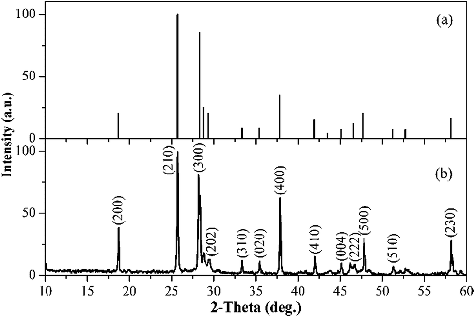
The crystal was pulverized and used for the phase identification, elemental analysis and Raman spectrum measurement. The X-ray powder diffraction (XPRD) pattern was collected on a powder diffractometer (DMAX2500, Rigaku) operating at 40 kV and 100 mA using Cu-Kα (λ = 1.54056 Å) radiation. It can be observed from Fig. 2 that all diffraction peaks match well with those of standard pattern of CGM (JCPDS card no. 41-0419). The Yb3+ concentration Ccrystal was determined to be 4.4 at% (atomic percent with respect to trivalent cation of the host) by means of the inductively coupled plasma optical emission spectrometry (Ultima 2, Jobin–Yvon), namely [Yb3+] = 2.25 × 10²⁰ ions cm−3. Given the Yb3+ concentration Cmelt is 5.0 at% in the starting melting, the segregation coefficient K of Yb3+ in the crystal, defined as K = Ccrystal/Cmelt, is 0.88. The Raman spectrum was measured on a Raman spectrometer (LabRAM HR800, Jobin–Yvon) with a frequency-doubled Nd3+:YAG laser (532 nm) at room temperature.
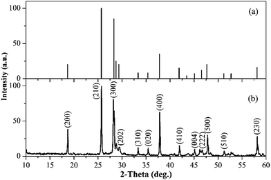 |
| | Fig. 2 The XPRD patterns of (a) JCPDS card no. 41-0419 and (b) the Yb3+:CGM crystal. | |
A piece of 0.8 mm thick cleavage plate with its main faces parallel to the (100) planes (Fig. 1c), was exfoliated from the as-grown crystal by a knife and directly used for the spectral measurements without polishing. The absorption spectra were recorded by a UV/VIS/NIR spectrometer (Lambda900, Perkin–Elmer). The 77- and 300 K excitation and fluorescence spectra as well as the decay curves were carried out on a fluorescence spectrophotometer (FLS920, Edinburgh) equipped with a 450 W continuous xenon lamp and a microsecond pulsed flashlamp.
3. Results and discussion
3.1 Cleavage habit and crystal structure
The as-grown crystals exhibit distinct cleavage behavior along the (100) planes, which can be explained by the layered structure.12,13 Fig. 1a reveals that the –Gd–(MoO4)–Cs–(MoO4)– alternative layers run along the a-axis. All these layers are parallel to the (100) planes and adjacent layers are linked by the Cs–O or Gd–O bonds. Obviously, the bond strengths are sorted in the order of Mo–O > Gd–O > Cs–O bonds, which indicates the Cs–O bonds are the most probable bonds to break. Therefore, the as-grown crystal has a tendency to cleavage along the (100) planes owing to the Cs–O bond rupture.
So far the typical thickness of the CGM crystal has been reported to be 1 mm at most.13,17 Much effort about crystal growth method and technique is still required to obtain crystals with large size. It should be noticed that the cleavage yields an interesting cleavage slice with smooth and parallel surfaces, as shown in Fig. 1c. The unprocessed cleavage slice can be used directly as a gain medium for microchip lasers.18,19 A microchip laser consists of a small piece of laser medium polished flat and parallel on two sides, and the cavity mirrors deposited directly onto the medium faces.20 The conventional fabrication processing includes slicing (to submillimeter thick wafers), polishing, coating and at last cutting (into 1 mm-square pieces). Each piece serves as a complete laser cavity. The cleavage technique is simpler than the conventional machining processing, since the slicing and polishing are dispensable for cleavage microchips. Effective laser operations have been realized in the unprocessed cleavage microchips of Nd3+:LaB3O6 (ref. 18) and Tm3+:BaGd2(MoO4)4.19
3.2 Absorption spectrum and lifetime
Fig. 3 exhibits the absorption spectrum of the Yb3+:CGM crystal at room temperature. The spectrum is composed of broad mutually overlapping bands. Three main absorption peaks centered at 962, 976 and 1006 nm arise from the electronic transitions between the Stark levels of the 2F7/2 and 2F5/2 manifolds of Yb3+, and the detailed assignment will be discussed on Section 3.3. The maximum absorption cross-section σabs amounts to 3.9 × 10⁻²⁰ cm2 at 976 nm, which far exceeds than those of Yb3+:NaGd(MoO4)2 (2.2 × 10⁻²⁰ cm2 for the π polarization at 975 nm)4 and Yb3+:LiGd(MoO4)2 (1.6 × 10⁻²⁰ cm2 for the π polarization at 975 nm).21 The full-widths at half-maximum (FWHM), another crucial factor affecting the pumping efficiency, reaches up to 8.1 nm for the Yb3+:CGM crystal. The value is much smaller than that of Yb3+:NaGd(MoO4)2 (50.0 nm)7 but larger than that of Yb3+:KGd(WO4)2 (3.7 nm).9 Such a broad bandwidth is qualified to improve the spectral overlap with the pump beam, accommodate the thermal drift of the pump wavelength and hence make the title crystal adequate for commercial InGaAs laser diode (LD) pumping.
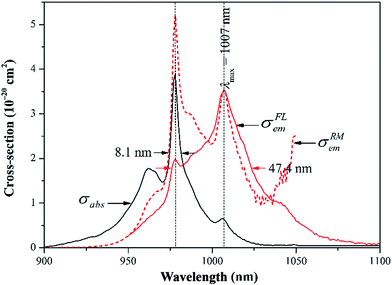 |
| | Fig. 3 Absorption and emission cross-sections calculated by the RM and FL method. | |
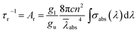
The absorption spectrum enables us to estimate the radiative lifetime τr of the 2F5/2 upper laser level by the following formula:14
| |
 | (1) |
where
c,
![[small lambda, Greek, macron]](https://www.rsc.org/images/entities/i_char_e0cc.gif) abs
abs and
g denote the velocity of light, the mean wavelength of absorption band. Since the Yb
3+ ion (4f
13 configuration) has an odd number of electrons in the 4f shell, the Stark levels are doubly degenerate in terms of the Kramer's degeneracy theorem. So the degeneracy
g turns out to be (2
J + 1)/2,
i.e.,
gu = 3 for
2F
5/2 (
J = 5/2) and
gl = 4 for
2F
7/2 (
J = 7/2). The refractive index
n is roughly taken as 2.0. Thus the
τr is determined to be 235 μs in this work.
The fluorescence decay curves were recorded under pulsed excitation at 976 nm and emission at 1039 nm, as shown in Fig. 4. It is universally known that the reabsorption and total internal reflection will elongate remarkably the measured fluorescence lifetime τf, especially for Yb3+ characterized with a large degree of overlap between absorption and emission. Not surprisingly, the τf (581 μs) for the bulk sample is significantly longer than the τr (235 μs). In the past few years, the powder method has been proved to be a simple and efficient approach to more accurately measure the intrinsic lifetime of the 2F5/2 manifold.7,8,22,23 The bulk sample is ground to fine powder and dispersed in the monochlorobenzene fluid (n = 1.52). Detailed experimental procedure has been provided elsewhere.8 In principle, a fluid with a refractive index close to that of the crystal (n ≈ 2) is desirable in order to eliminate the total internal reflection. But the fluids with high n are toxic. So the monochlorobenzene (n = 1.52) has been chosen for refractive-index matching in this work. As expected, the powder method yields much shorter τf (274 μs) than that for the bulk sample (581 μs). The quantum yield, defined as η = τf/τr, is slightly greater than 1. One possible explanation is that the powder method cannot eliminate the reabsorption and total internal reflection completely, resulting in the overestimated τf.22,23 Anyway, the result indicates high η for the Yb3+:CGM crystal, which implies that nonradiative relaxation is rather inefficient.
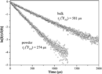 |
| | Fig. 4 Fluorescence decay curves for bulk and power samples of the Yb3+:CGM crystal. | |
3.3 Excitation and emission spectra
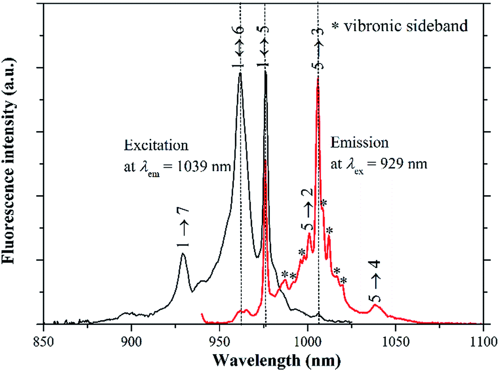
The electronic transitions only involve two manifolds due to the simple 4f13 electronic configuration of Yb3+, i.e., the 2F7/2 ground state and 2F5/2 excited state separated by about 10000 cm−1. The C2 site symmetry of Yb3+ in the CGM crystal is expected to split the two manifolds into four and three doubly degenerate Stark levels, respectively. Here the Stark levels are labelled as numbers from 1 to 4 for the 2F7/2 manifold and from 5 to 7 for the 2F5/2 manifold in the order of the increasing energy.
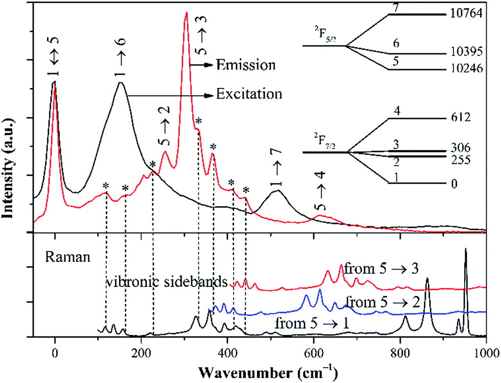
The low-temperature excitation and emission spectra are recorded at 77 K to reduce the spectral broadening and further determine the energies of Stark levels, as illustrated in Fig. 5. The common excitation and emission lines at 976 nm (10246 cm−1) are readily assigned to be resonant zero-phonon line transition between the lowest Stark levels of the 2F7/2 and 2F5/2 manifolds (1 ↔ 5). The other two well-resolved excitation lines at 962 nm (10395 cm−1) and 929 nm (10764 cm−1) are attributed to the electronic transitions 1 → 6 and 1 → 7, respectively. Different from the excitation spectrum, the emission spectrum displays more transition lines than expected. Obviously, some spectral lines in the 980–1030 nm spectral region, should belong to the vibronic sidebands originating in the strong electron-phonon interaction of Yb3+ with the lattice vibrations.23,24 Given that the phonon sidebands should appear at longer wavelength than the corresponding electron transition in the emission spectrum,23 these lines can only be associated with the 5 → 1, 5 → 2 or 5 → 3 electronic transitions. Keeping in mind the hypothesis that the Raman spectrum should reflect vibronic structures accompanying each pure electronic transition, the Raman spectrum is introduced to aid the interpretation of the electronic levels.23 Fig. 6 compares the excitation and emission spectra with the Raman spectrum, with an aim to distinguish the vibronic transitions from pure electronic transitions. These spectra are adjusted to the same energy scale. The energy origins of the excitation and emission spectra are taken at 5 ↔ 1 transition, while three energy onsets of Raman spectrum are selected to identify the possible vibronic sidebands from the 5 → 1, 5 → 2 and 5 → 3 transitions, respectively. The common spectral lines in the emission and Raman spectra are marked by asterisks in Fig. 6 and interpreted as the vibronic sidebands, while the remaining lines which are present in the emission spectrum but absent in the Raman spectrum, belong to the electronic transitions.
 |
| | Fig. 5 Excitation and emission spectra of the Yb3+:CGM crystal at 77 K. | |
 |
| | Fig. 6 Comparison of 77 K excitation and emission spectra with 300 K Raman spectrum. For Raman spectrum, three positions of the origin have been considered from the 5 → 1, 5 → 2 and 5 → 3 transition lines, respectively. The inset indicates the distribution of Stark levels of Yb3+ in the CGM crystal. | |
Eventually, the sequence of Yb3+ energy levels is established as follows: 2F7/2 = 0, 255, 306, 612 cm−1, and 2F5/2 = 10246, 10395 and 10764 cm−1, as sketched in the inset of Fig. 6. To our knowledge, the overall splitting for the 2F7/2 manifold (ΔE = 612 cm−1) is the largest among the DMo and DW ever reported except Yb3+:LiLu(WO4)2 (ΔE = 749 cm−1).25 The high ΔE stems from a strong crystal field characterized by a low point symmetry (C2) and a large distribution of Gd(Yb)–O distances, which is beneficial to limit thermal population of the terminal laser level and reduce the threshold pumping power.
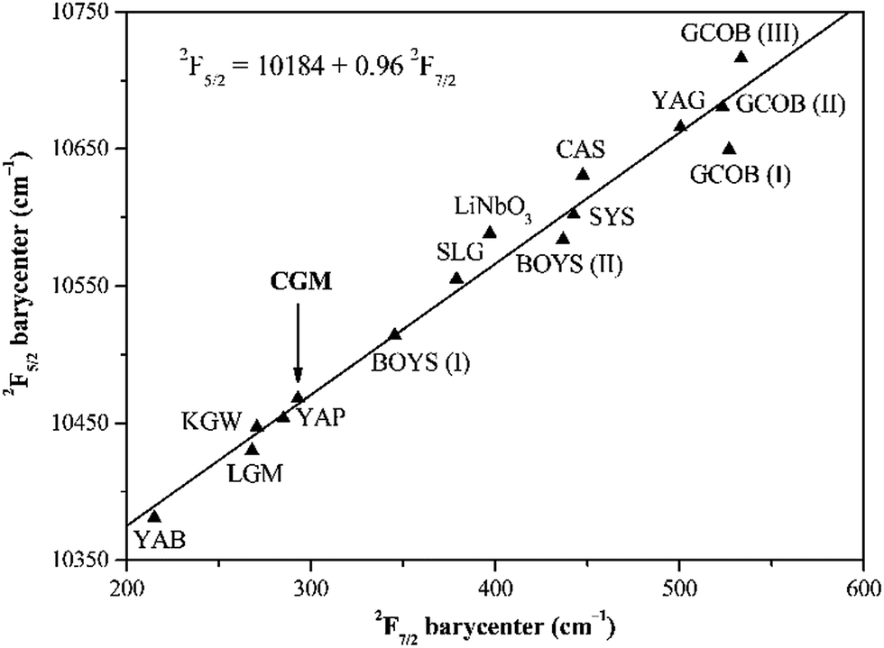
Our assignment is verified by the ‘barycenter plot’ method proposed by E. Antic-Fidancev.26 In principle, the energy separation between the 2F7/2 and 2F5/2 manifolds should be constant whatever the matrix. In other words, the 2F5/2 barycenter as a function of the 2F7/2 barycenter should obey a linear relationship with a slope of unity.22–24 Fig. 7 presents the evolution of the 2F5/2 barycenter with the 2F7/2 barycenter for various Yb3+-doped crystals. The representative point for the title crystal is well-aligned with the theoretical line, confirming our interpretation.
 |
| | Fig. 7 A barycenter plot for various Yb3+-doped crystalline materials. | |
Knowledge of the Stark levels makes it possible to estimate the emission cross-section σem from the absorption spectrum in accordance with the reciprocity method (RM):27
| | |
σRMem(λ) = σabs(λ)(Zl/Zu)exp[(Ezl − hc/λ)/kBT]
| (2) |
where
Ezl denotes the zero-phone line energy,
kB is the Boltzmann constant,
Zl and
Zu denote the partition functions of the lower
2F
7/2 and the upper
2F
5/2 manifolds, which are given by:
| | |
Zk = ∑dkexp(−Ek/kBT)
| (3) |
where
dk and
Ek are the degeneracy and the energy of the Stark level
k. The ratio
Zl/
Zu is 1.34 and
Ezl is 10
246 cm
−1 in the present work.
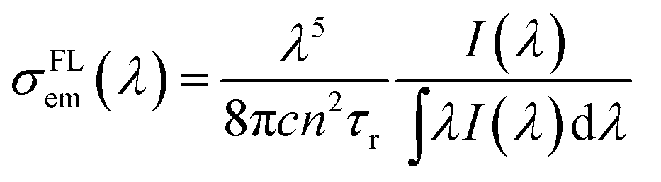
The RM is valid only in the vicinity of the fundamental transition where there is significant absorption.14 The absorption is so low at long-wavelength wing of the absorption spectrum that even a noise will be magnified exponentially in terms of eqn (2). The RM is no longer reliable at longer wavelengths, and this is the reason why the σRMem increases abnormally at λ > 1025 nm in Fig. 3. The σRMem in the long-wavelength range can be corrected by the Füchtbauer–Ladenburg (FL) formula:28
| |
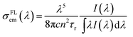 | (4) |
where
I(
λ) denotes the fluorescence intensity as a function of the wavelength
λ.
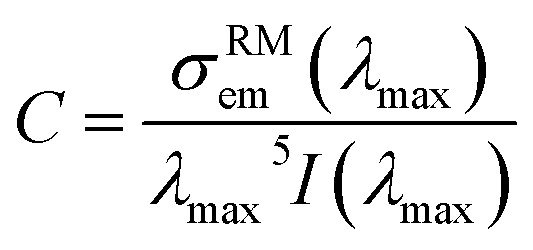
The FL relationship also has its limitations: it is valid only in the spectral region where there is no reabsorption.13 It should be noted that the reabsorption decreases the fluorescence intensity, resulting in an underestimate of the integral in eqn (4). For this reason, the eqn (4) is rewritten as:29
where
C represents all factors independent of wavelength and can be quantified by:
29| |
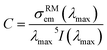 | (6) |
where
λmax = 1007 nm in this work corresponds to the wavelength at which both RM and FL are applicable.
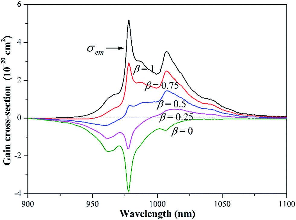
The combination of the RM and FL methods can circumvent their shortcomings and describe precisely the wavelength dependence of the σem in the whole spectral region, as shown in Fig. 3. The σRMem is more reliable at λ < 1007 nm, while σFLem is more accurate at λ > 1007 nm. The σem are equal to 3.6 × 10⁻²⁰ at 1007 nm and 1.0 × 10⁻²⁰ cm2 at 1038 nm, respectively. The corrected σem is subsequently used to calculate the gain cross-section σg(λ), which is defined as:
| | |
σg(λ) = βσem(λ) − (1 − β)σabs(λ)
| (7) |
where
β denotes the fraction of ions in the excited state. The FWHM of gain band is a measure of the wavelength tunability of a material for tunable or ultrafast laser applications.
30 The FWHM of gain band at
β = 0.5 is as high as 39 nm (
Fig. 8), which is superior to those of Yb
3+:YAG (9 nm) and Yb
3+:KGd(WO
4)
2 (25 nm)
31 and comparable to those of Yb
3+:NaLa(MoO
4)
2 (41 nm)
7 and Yb
3+:NaGd(MoO
4)
2 (43 nm).
7 The Yb
3+ bandwidths is known to be particularly host dependent and influenced by the splitting of energy level, electron-phonon coupling, structural disorder or multisites character of the host.
14,31 The latter two are excluded on the basis of the crystal structure. The combination of large splitting of energy level and strong electron-phonon coupling, are the most probable explanation for such a broad FWHM. The minimum theoretical duration Δ
tmin is derived as 27 fs according to the Fourier inequality Δ
νΔ
t ≥ 0.315 (sech
2-shape pulse), indicating that the crystal permits the generation of sub-100 fs laser pulses.
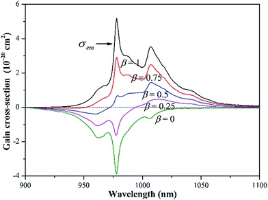 |
| | Fig. 8 Gain cross-section spectrum of the Yb3+:CGM crystal for different inversion ratios β. | |
3.4 Evaluation of the laser potential
The laser performance of the Yb3+:CGM crystal, can be estimated by the laser parameters: βmin, Isat and Imin.28 βmin denotes the minimum inversion fraction of Yb3+ ions that must be excited to balance exactly the gain with the ground-state absorption at the extraction wavelength λext. The pump saturation intensity Isat describes the capability to get the usual bleaching phenomena in laser physics. Imin stands for the minimum pump intensity required for transparency at the extraction wavelength λext. They can be calculated by the following equations:28| |
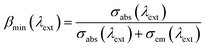 | (8) |
| |
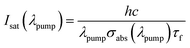 | (9) |
| | |
Imin = βmin(λext)Isat(λpump)
| (10) |
If λpump = 976 nm and τf = 274 μs are selected, the Isat are calculated to be 19.0 kW cm−2. Then the Imin are determined to be 2.9 kW cm−2 for λext = 1007 nm and 0.8 kW cm−2 for λext = 1038 nm, respectively.
The important structural and spectroscopic parameters of the Yb3+:CGM crystal are summarized in Table 1 and compared with those of other Yb3+-doped DMo and DW crystals. From the spectroscopic point of view, the Yb3+:CGM crystal is situated at the intermediate position between the disordered tetragonal and ordered monoclinic DMo and DW crystals. Until now, sub-100 fs laser pulses have already been demonstrated in Yb3+:KGd(WO4)2 (78 fs),34 Yb3+:NaY(WO4)2 (53 fs)35 and Yb3+:NaY(MoO4)2 (91 fs).36 The production of ultrafast pulses is known to depend critically on the optical bandwidths of gain media.31,37 From this prospective, the disordered tetragonal DMo and DW are more advantageous to deliver shorter pulse duration and higher peak power as compared with the ordered monoclinic ones. But the former suffers from low optical cross-sections and hence a low gain. A tradeoff between optical bandwidths and emission cross-sections is achieved in the case of the Yb3+:CGM crystal. In addition, the crystal is suitable for LD pumping at 976 nm due to broad absorption bandwidth (FWHM = 8.1 nm), and operates in a quasi-three-level scheme with large ground-state splitting (ΔE = 612 cm−1). And lastly, an unprocessed cleavage slice can be used directly for microchip lasers, simplifying fabrication processes. The unique combination of above-listed advantages proposes the potential application of the Yb3+:CGM crystal in the LD-pumped microchip laser systems capable to produce the tunable and sub-100 fs pulsed laser.
Table 1 Structural and spectroscopic features of several promising Yb3+-doped laser crystalsa
| Crystals |
NGM |
NGW |
KGW |
CGM |
| Notes: Czochralski (Cz.), NaGd(MoO4)2 (NGM), NaGd(WO4)2 (NGW), KGd(WO4)2 (KGW). |
| Growth method |
Cz. |
Cz. |
TSSG |
TSSG |
| Space group |
I41/a |
I![[4 with combining macron]](https://www.rsc.org/images/entities/char_0034_0304.gif) |
C2/c |
P2/c |
| Multisite or disorder |
√ |
√ |
× |
× |
| Symmetry (Gd) |
S4 |
S4 |
C2 |
C2 |
| ΔE (2F7/2) (cm−1) |
<500 |
492 |
535 |
612 |
| λabs (nm) |
975 |
975 |
981 |
976 |
| Δλabs (nm) |
50 |
50 (π) |
3.7 |
8.1 |
| 43 (σ) |
| σabs (10−20 cm2) |
2.2 (π) |
1.78 (π) |
12.0 |
3.9 |
| 1.36 (σ) |
| λem (nm) |
1000 |
1000 |
1023 |
1007 |
| 1038 |
| Δλ*em (nm) |
43 |
40 (π) |
25 |
39 |
| σem (10−20 cm2) |
2.7 (π) |
1.89 (π) |
2.8 |
3.6 |
| 1.4 (σ) |
0.75 (σ) |
1.0 |
| τf (μs) |
280 |
320 |
317 |
274 |
| Δtmin (fs) |
24 |
26 |
44 |
27 |
| Isat (kW cm−2) |
33.1 (π) |
35.7 (π) |
5.3 |
19.0 |
| Reference |
4, 7 |
32, 33 |
9, 31 |
This work |
4. Conclusions
The crystal growth, morphology and spectroscopic properties of a layered Yb3+:CGM crystal have been systemically investigated in order to assess its laser potential. The cleavage habit and spectroscopic properties have been found to be closely associated with the crystal structure: Firstly, the highly distorted coordination environment of Yb3+ contributes to the most largest ground-state splitting of Yb3+ among the DMo and DW crystals ever reported other than Yb3+:LiLu(WO4)2, which is favorable for low-threshold quasi-three-level laser operation; secondly, single site and structure order give rise to high transition cross-sections and modest absorption bandwidth. The emission/gain bandwidth is remarkably high due to the strong electron-phonon coupling and large energy-level splitting, which is promising for tunable and ultrafast (sub-100 fs) pulse laser applications. Thirdly, the anisotropic layered structure is responsible for the perfect cleavage along the (100) planes. A high-quality cleavage slice is too thin to be used as a laser rod in laser cavity, but is well suited for microchip laser configuration. In conclusion, the Yb3+:CGM crystal can be regarded as a potential gain medium for microchip lasers.
Acknowledgements
We gratefully acknowledge the financial support of the NSF of China (61205213, 21201071 and 21176099), the NSF of Anhui Province (1208085QB42), the Science and Technology Project of Huainan City (2013A4105), and the Program for Innovative Research Team in Huainan Normal University.
Notes and references
- J. R. de Moraes, F. R. da Silva, L. Gomes, V. L. Mazzocchi, C. B. R. Parente and S. L. Baldochi, CrystEngComm, 2013, 15, 2260 RSC.
- A. McKay, O. Kitzler and R. P. Mildren, Opt. Express, 2014, 22, 707 CrossRef PubMed.
- A. García-Cortés, C. Cascales, A. D. Andrés, C. Zaldo, E. V. Zharikov, K. A. Subbotin, S. Bjurshagen, V. Pasiskevicius and M. Rico, IEEE J. Quantum Electron., 2007, 43, 157 CrossRef.
- E. V. Zharikov, C. Zaldo and F. Díaz, MRS Bull., 2009, 34, 271 CrossRef CAS.
- V. Volkov, C. Cascales, A. Kling and C. Zaldo, Chem. Mater., 2005, 17, 291 CrossRef CAS.
- J. M. Cano-Torres, M. Rico, X. Han, M. D. Serrano, C. Cascales, C. Zaldo, V. Petrov, U. Griebner, X. Mateos, P. Koopmann and C. Kränkel, Phys. Rev. B: Condens. Matter Mater. Phys., 2011, 84, 174207 CrossRef.
- Y. K. Voron'ko, K. A. Subbotin, V. E. Shukshin, D. A. Lis, S. N. Ushakov, A. V. Popov and E. V. Zharikov, Opt. Mater., 2006, 29, 246 CrossRef PubMed.
- M. C. Pujol, M. A. Bursukova, F. Güell, X. Mateos, R. Solé, J. Gavaldà, M. Aguiló, J. Massons, F. Díaz, P. Klopp, U. Griebner and V. Petrov, Phys. Rev. B: Condens. Matter Mater. Phys., 2002, 65, 165121 CrossRef.
- N. V. Kuleshov, A. A. Lagastky, A. V. Podolipensky, V. P. Milkhailor and G. Huber, Opt. Lett., 1997, 22, 1317 CrossRef CAS.
- V. A. Isupov, Ferroelectrics, 2005, 321, 63 CrossRef CAS.
- W. Zhao, W. Zhou, M. Song, G. Wang, J. Du, H. Yu, Y. Chen and J. Chen, J. Cryst. Growth, 2011, 332, 87 CrossRef CAS PubMed.
- P. Shi, Z. Xia, M. S. Molokeev and V. V. Atuchin, Dalton Trans., 2014, 9669 RSC.
- V. Tkáč, A. Orendáčová, R. Tarasenko, E. Čižmár, M. Orendíáč, K. Tibenská, A. G. Anders, S. Gao, V. Pavlík and A. Feher, J. Phys.: Condens. Matter, 2013, 25, 5006001 CrossRef PubMed.
- P. Haumesser, R. Gaumé, B. Viana and D. Vivien, J. Opt. Soc. Am. B, 2002, 19, 2365 CrossRef CAS.
- M. C. Pujol, M. Rico, C. Zaldo, R. Solé, V. Nikolov, X. Solans, M. Aguiló and F. Díaz, Appl. Phys. B, 1999, 68, 187 CrossRef CAS.
- N. V. Ivannikova, L. P. Kozeeva and A. A. Pavlyuk, Inorg. Mater., 1988, 24, 379 Search PubMed.
- G. A. Zvyagina, V. D. Fil', Yu. N. Kharchenko and N. M. Nesterenko, J. Low Temp. Phys., 2004, 30, 236 CrossRef CAS PubMed.
- Y. J. Chen, Y. D. Huang, X. Q. Lin, Q. G. Tan, Z. D. Luo and Y. F. Lin, Appl. Phys. Lett., 2005, 86, 021115 CrossRef PubMed.
- H. Zhu, Y. Chen, Y. Lin, X. Gong, Z. Luo and Y. D. Huang, J. Opt. Soc. Am. B, 2008, 25, 801 CrossRef CAS.
- J. J. Zayhowski, Opt. Mater., 1999, 11, 255 CrossRef CAS.
- M. Rico, U. Griebner, V. Petrov, P. Ortega, X. Han, C. Cascales and C. Zaldo, J. Opt. Soc. Am. B, 2006, 23, 1083 CrossRef CAS.
- W. Zhao, W.-W. Zhou, B. Wei and G.-F. Wang, Phys. Status Solidi A, 2013, 210, 367 CrossRef CAS PubMed.
- M. Ito, G. Boulon, A. Bensalah, Y. Guyot, C. Goutaudier and H. Sato, J. Opt. Soc. Am. B, 2007, 24, 3023 CrossRef CAS.
- G. Boulon, J. Alloys Compd., 2008, 451, 1 CrossRef CAS PubMed.
- M. Derbal, D. Ouadjaout, F. Siserir, V. Jubera, J. P. Chaminade, A. Garcia, O. Viraphong and M. K. Hannifi, Opt. Mater., 2010, 32, 756 CrossRef CAS PubMed.
- E. Antic-Fidancev, J. Alloys Compd., 2001, 300–301, 2 Search PubMed , barycenter.
- D. E. McCumber, Phys. Rev., 1964, 136, A954 CrossRef.
- L. D. DeLoach, S. A. Payne, L. L. Chase, L. K. Smith, W. L. Kway and W. F. Krupke, IEEE J. Quantum Electron., 1993, 29, 1179 CrossRef CAS.
- W. Ryba-Romanowski, S. Go Gołab, I. Sokólska, G. Dominiak-Dzik, J. Zawadzka, M. Berkowski, J. Fink-Finowicki and M. Baba, Appl. Phys. B, 1999, 68, 199 CrossRef CAS.
- S. Chénais, F. Druon, F. Balembois, P. Georges, R. Gaumé, P. H. Haumesser, B. Viana, G. P. Aka and D. Vivien, J. Opt. Soc. Am. B, 2002, 19, 1083 CrossRef.
- F. Druon, F. Balembois and P. Georges, C. R. Phys., 2007, 8, 153 CrossRef CAS PubMed.
- Y. Cheng, X. B. Yang, Z. Xin, S. S. Cheng, D. H. Cao, X. D. Xu and J. Xu, Laser Phys., 2009, 19, 216 Search PubMed.
- C. Cascales, M. D. Serrano, F. Esteban-Betegón, C. Zaldo, R. Peters, K. Petermann, G. Huber, L. Ackermann, D. Rytz, C. Dupré, M. Rico, J. Liu, U. Griebner and V. Petrov, Phys. Rev. B: Condens. Matter Mater. Phys., 2006, 74, 174114 CrossRef.
- H. Zhao and A. Major, Opt. Express, 2014, 22, 30425 CrossRef CAS PubMed.
- A. García-Cortés, J. M. Cano-Torres, M. D. Serrano, C. Cascales, C. Zaldo, S. Rivier, X. Mateos, U. Griebner and V. Petrov, IEEE J. Quantum Electron., 2007, 43, 758 CrossRef.
- A. Schmidt, S. Rivier, V. Petrov, U. Griebner, X. Han, J. M. Cano-Torres, A. García-Cortés, M. D. Serrano, C. Cascales and C. Zaldo, J. Opt. Soc. Am. B, 2008, 25, 1341 CrossRef CAS.
- L. Li, Y. Yu, G. Wang and L. Z. Zhang, RSC Adv., 2014, 4, 37041 RSC.
|
| This journal is © The Royal Society of Chemistry 2015 |
Click here to see how this site uses Cookies. View our privacy policy here.