
High quality sub-10 nm graphene nanoribbons by on-chip PS-b-PDMS block copolymer lithography†
Sozaraj Rasappaab,
José M. Caridadab,
Lars Schulteab,
Alberto Caglianiab,
Dipu Borahcd,
Michael A. Morriscd,
Peter Bøggildab and
Sokol Ndoni*ab
aDepartment of Micro and Nanotechnology, Technical University of Denmark, DK-2800 Kgs. Lyngby, Denmark. E-mail: sond@nanotech.dtu.dk; Tel: +45 4525 8146
bCenter for Nanostructured Graphene, CNG, Technical University of Denmark, DK-2800 Kgs. Lyngby, Denmark
cMaterials Section, Department of Chemistry, University College Cork, Cork, Ireland
dAMBER, Trinity College Dublin, Dublin-2, Ireland
First published on 29th July 2015
Abstract
A block copolymer self-assembly holds great promise as a rapid, cheap and scalable approach to nanolithography. We present a straightforward method for fabrication of sub-10 nm line patterns from a lamellar polystyrene-b-polydimethylsiloxane (SD) block copolymer with a total average molecular weight of 10.5 kg mol−1. Thin SD films directly spin cast onto silicon substrates and on graphene, form regular line patterns of sub-10 nm pitch on the substrates after a few minutes of annealing at 45 °C in the presence of toluene vapour. Perfect pattern alignment was achieved by confining the films inside the trenches of graphoepitaxial substrates. The SD template was furthermore used as a lithographic mask to fabricate high-quality sub-10 nm graphene nanoribbons. This was realized by one step oxygen plasma treatment, which accomplishes three tasks: hardening the PDMS block by oxidation, and etching both the PS block and the graphene under PS. Raman analysis supports the formation of graphene nanoribbons with an average distance between defects corresponding to the oxidized PDMS pitch, with no sign of defects generated in the ribbon channel. This suggests a high degree of protection of the nanoribbons by the hard oxidized PDMS mask formed in situ during oxygen plasma etching.
Introduction
While the need for fast and accurate nanostructuring has primarily been driven by the semiconductor industry,1–4 the appearance of novel 2D materials has highlighted this area as more critical than ever, as nanopatterning of these materials is one of the most important means of tuning their electrical, chemical and optical properties.5 The most versatile and widely studied of these materials is graphene: a one atom thick material composed of only sp2 bonded carbon in which charge carriers behave as relativistic particles.6 Graphene exhibits extremely high carrier mobility and for that reason is considered as a highly promising candidate for future fast and densely packed electronics.5 However, graphene is a zero-bandgap semiconductor; it is therefore not possible to effectively switch off the electrical current by changing the applied gate voltage, which is a basic operation for field effect transistors, the building block of integrated circuits.7–9 In contrast, graphene nanoribbons (GNR) and graphene nanomesh/antidot lattices (GAL) have been predicted to be two possible modifications that exhibit a band gap.10,11 Experiments so far have shown how diminishing GNR width results in an increased transport gap12–14 particularly at low temperatures, however, no clear proof of an actual energy band gap has been experimentally reported yet for lithographically defined nanoribbons.15 A key parameter affecting the charge transport in graphene nanoribbons is the amount of defects introduced in the GNR channel during fabrication,16 which could be determinant in the realization of a real energy band gap in the monolayer material. In the present study we realize sub-10 nm GNRs, which through an enhanced protection from a hardened block copolymer based mask, exhibit the traits of a defect free channel. The latter is proved by Raman spectroscopy, which indicates that the disorder existent in the nanostructures can be accounted for by the inevitable etch disorder,17,18 thus the SD processing avoids the introduction of defects in the ribbon channel.Block copolymer based nanolithography has been gaining momentum as a viable alternative to photolithography for large area, ultra-dense nanofabrication,18,19 and in the ITRS 2013 roadmap, directed self-assembly (DSA) using block copolymers is highlighted as a key enabling technique for front end lithography. The device feature size is finally defined by the polymer chain length of block copolymers and this can be varied by synthesis of each BCP.20 Block copolymers with higher Flory–Huggins interaction parameter χ self-assemble at relatively lower total molecular weight, consenting to realize smaller feature sizes. In addition, comparing two block copolymers with similar self-assembled feature sizes the BCP with higher χ will show better segregation between the blocks, which is equivalent with a sharper interface between the blocks and ultimately with better defined lithographic pattern transfer.21 For these reasons PS-b-PDMS block copolymers with the relatively high χ = 0.29 at room temperature, have been the subject of many studies in the recent years. Sub-10 nm features and sub-20 nm periods are easily realized by such block copolymers, while the very popular block copolymers of composition PS-b-PMMA with χ = 0.06 cannot form self-assembled patterns at these reduced length-scales.22
Controlling the out-of-plane and in-plane alignment of block copolymer thin films is generally challenging due to the complexity of the interplay between the block segregation and interface energies.22,23 The most popular strategy to control the out-of-plane BCP arrangement is to chemically modify the substrate with a neutral brush layer, thus avoiding the preferential wetting of the substrate by any of the blocks.24 Apart from complicating the overall procedure, which is always costly at these length scales, this step shows some essential drawbacks and in the best case only partially helps controlling the vertical alignment of the BCP on the substrate. Firstly, air or vacuum at the BCP–air interface is in most cases not neutral relative to the blocks, with the noticeable exception of PS-b-PMMA annealed at around 200 °C;20 in the case of PS-b-PDMS the PDMS block with the lowest surface energy will tend at equilibrium conditions to cover the polymer–air interface.25 Secondly, there are substrates like graphene that are unsuited for chemical modification by grafting of a neutral layer, as this would lead to adverse effects such as changes in band structure or doping.26 In such cases another step of substrate coverage with e.g. a silica thin layer has been applied, which then can be used for grafting of a neutral brush layer.26 This further complicates the sample preparation procedure and the etching process. Thirdly, the choice of the brush layer composition as neutral surface for a given block copolymer requires fine tuning, thus rendering the procedure highly non robust; even different batches of essentially the same block copolymer may require readjustment of the brush layer composition.
In the present study we demonstrate self-assembly of a lamellar SD block copolymer directly on silicon and graphene substrates, without any preliminary substrate surface treatment. The use of solvent vapor annealing allows creation of regular line patterns without an upper/lower PDMS wetting layer. In the case of graphene we also show that the mask pattern can be transferred to graphene by direct application of oxygen plasma on the spin cast and annealed block copolymer. Remarkably, the oxygen plasma in this case fulfills three functions: (1) etching of the PS block, (2) hardening by oxidation of the PDMS block, (3) etching of graphene under the PS domains. Raman estimations of the graphene crystallite size are in excellent agreement with the width of the BCP trenches measured by SEM (both ∼10 nm), indicating that the etching process is ‘clean’ and does not introduce additional point defects in the channel of the nanostructured graphene. This is in marked contrast with competing top-down techniques based on electron beam lithography (EBL) and/or gas-phase chemical narrowing of the ribbons,16,27 where additional defects are inserted in the ribbon channel degrading their structural quality and modifying their electronic properties.16,27 Both, the high-density capability and the absence of undesired point defects in the channel of the here presented graphene nanoribbons proves the suitability of the PS-b-PDMS BCP lithography technique for graphene patterning at wafer scale.
Results and discussion
Fig. 1 illustrates the overall process of PS-b-PDMS (5k–5.5k) block copolymer based nanopatterning on planar silicon substrate, topographically patterned silicon substrate and graphene substrate. No surface pre-treatment or application of any brush layer prior to BCP deposition was necessary. As mentioned in Fig. 1 all the BCP coated films were solvo-thermally annealed to induce pattern formation.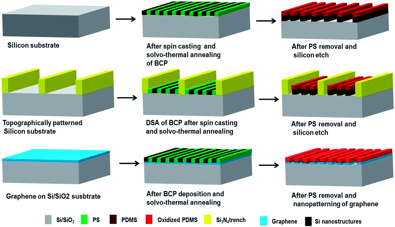 | ||
| Fig. 1 Schematics showing the process flow of BCP lithography for nanopatterning of graphene. | ||
The block copolymer thin films of PS-b-PDMS were spin-coated at a spin speed of 3200 rpm for 30 s, annealed at different conditions, and finally subject to PS removal and oxidation of PDMS. Fig. 2 shows a set of samples where the annealing temperature was varied between 22 °C (room temperature) and 55 °C, and the annealing time between 5 min and 20 min. The success of the proposed method relies on identifying the process window within which the line pattern is fully developed with minimal dewetting. We found that samples annealed at 45 °C for 15 min exhibit a highly ordered lamellar SD patterns as also shown in the corresponding image in Fig. 2. The quality and spacing of the line pattern is similar for all the images shown at the right-bottom quadrant of Fig. 2, i.e. at annealing times of 15–20 min and at temperatures of 45–55 °C. However, minimum dewetting was observed at a narrow window of approximately ±2 min and ±2 °C around the optimum conditions, which can be defined as the process window for the present procedure. Annealing at room temperature resulted into poorly defined patterns for all the annealing times. The annealing process depends on a combination of two major effects: (1) PS has a higher surface tension (γC = 32.8 mN m−1) than PDMS PS (γC = 24 mN m−1) that would lead to preferential PDMS surface segregation; (2) this may be compensated by the fact that the annealing solvent is toluene, δHildebrand ≡ δH = 18.2 (MPa)1/2, which is a preferential solvent for PS, δH = 18.7 (MPa)1/2, over PDMS, δH = 14.9 (MPa)1/2. At 22 °C the toluene vapour pressure is low and insufficient in the studied time window to compensate for the PDMS surface segregation, while the compensation is realized at the higher temperatures. The line pattern persistence length shows some variation for independently prepared samples, even at the optimum process window.
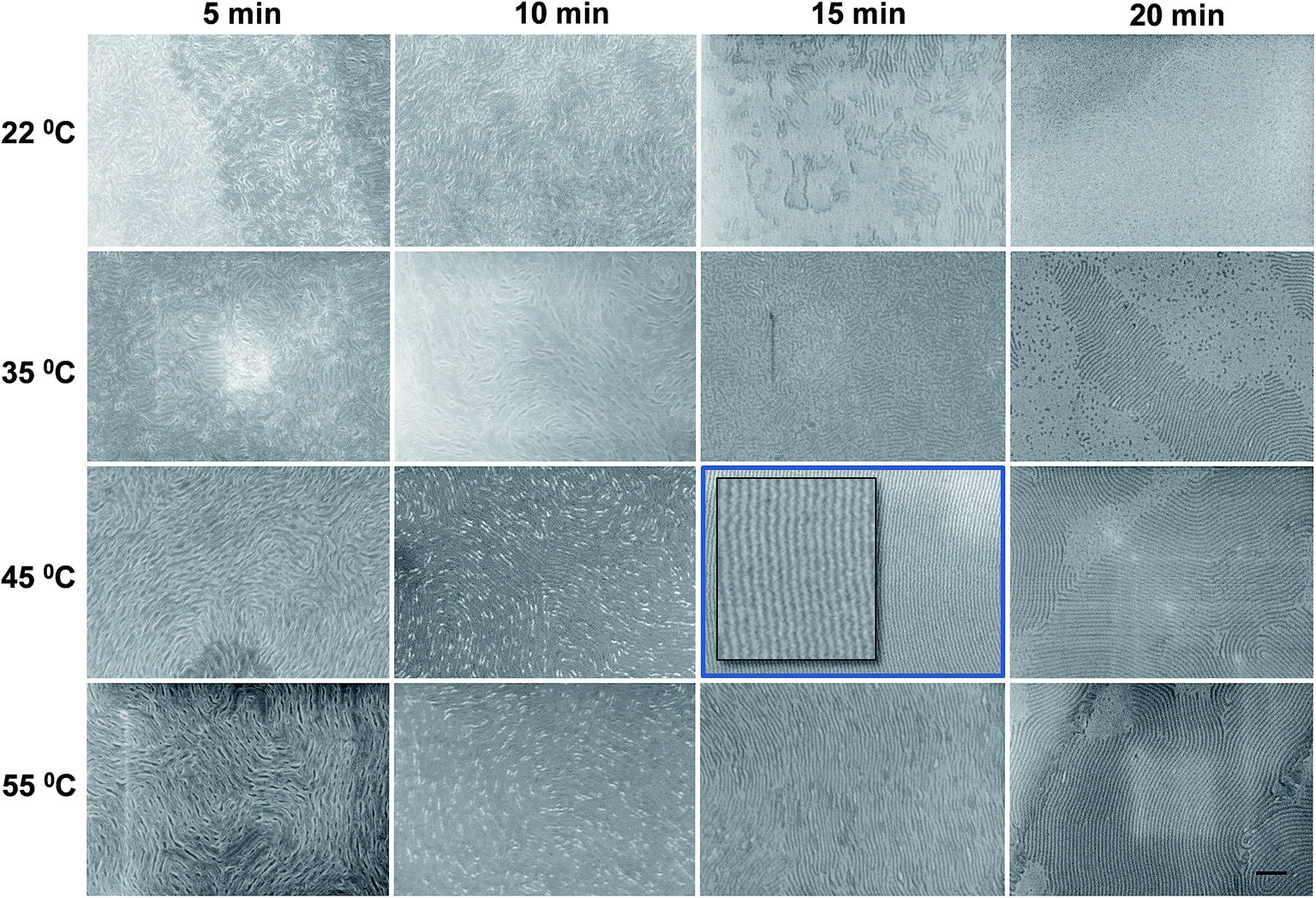 | ||
| Fig. 2 Top-down SEM images of lamellar PS-b-PDMS (5k–5.5k) spin coated on silicon substrate at 3200 rpm for 30 s and annealed, after PS removal. Left to right: annealed from 5 min to 20 min. Top to bottom: annealed at 22 °C to 55 °C. The highlighted SEM image at 45 °C for 15 min shows the best ordered and regular BCP patterns. All images have 200 nm scale bars. | ||
Fig. 3A shows the top down SEM image of wafer-wide silicon nanofins fabricated through SD with oxidised PDMS on top of it. Highly regular line spacing patterns with sub-10 nm features were obtained without any application of brush layer. Typically, this kind of regular alignment can be achieved by chemoepitaxial or graphoepitaxial (directed) self-assembly, DSA, with application of brush layer.28 Examples of DSA of our SD without any brush layer are shown in Fig. 3B–E. It is remarkable that direct spin casting of our SD onto flat silicon wafer followed by fast solvo-thermal annealing produces highly aligned line patterns as illustrated in Fig. 3A. CA Ross and co-worker's made significant progresses in graphoepitaxy using PS-b-PDMS systems but it must be noted that polymer brushes have been applied in all cases to induce vertical alignment.28 Here we demonstrate the confinement of 1–9 PDMS lines inside trenches of varying width. The top down SEM images in Fig. 3B–E show a variation of SD pitch size as the trench width decreases from 200 nm to 30 nm. PS preferentially wets the trench side walls. The pitch size in the 200 nm trenches is 22 nm, which is only slightly higher than the pitch size of 21 nm in the open area. The incommensurability between the natural SD period of 21 nm and the trench width increases with the decreasing of the trench width, reaching a maximum of 43% wider trench than the natural SD period. At the same time the wall roughness increases for the narrower trenches. It is amazing that the SD adapts to the large incommensurability and conforms to the trench width variations. This hints to a large enthalpy of adsorption of the PS block to the trench walls that can compensate for the unfavourable entropy of chain strain.
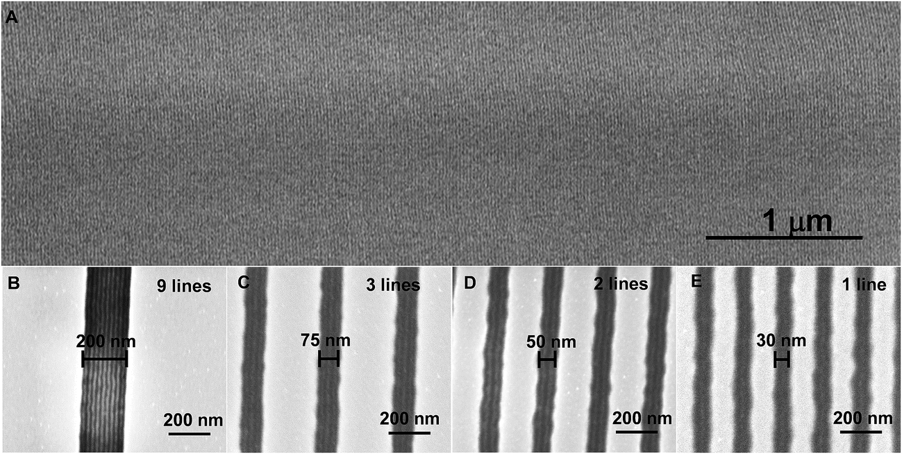 | ||
| Fig. 3 Top-down SEM images of silicon nanofins on planar and topographically patterned silicon substrates. (A) Low magnification SEM image of silicon nanowires on planar substrate fabricated via brushless self-assembly of PS-b-PDMS. (B–E) Topographically patterned silicon substrate with different trench width shows the confinement of oxidised PDMS structures. | ||
Raman analysis of graphene nanoribbons
Fig. 1 schematically describes the array of GNR fabrication using lamellar SD. Graphene thin film was grown on a Cu foil using chemical vapour technique (CVD) and then transferred to a p-doped Si wafer with 300 nm thick thermally grown SiO2 on top. Direct spin casting and solvo-thermal annealing of PS-b-PDMS created regular line patterns on the graphene substrate, as shown in Fig. 4A. This process is similar to the silicon substrate previously discussed, although in this case the regular lines appear at random places within the entire substrate area. The line direction and persistence length can be controlled by e.g. graphoepitaxy, similarly to the already presented case of silicon substrate. Graphoepitaxy with SU-8 ridges is a single-step lithography approach allowing to control the position and orientation of BCP line array patterns and of the fabricated GNRs as shown in Fig. SI.1.†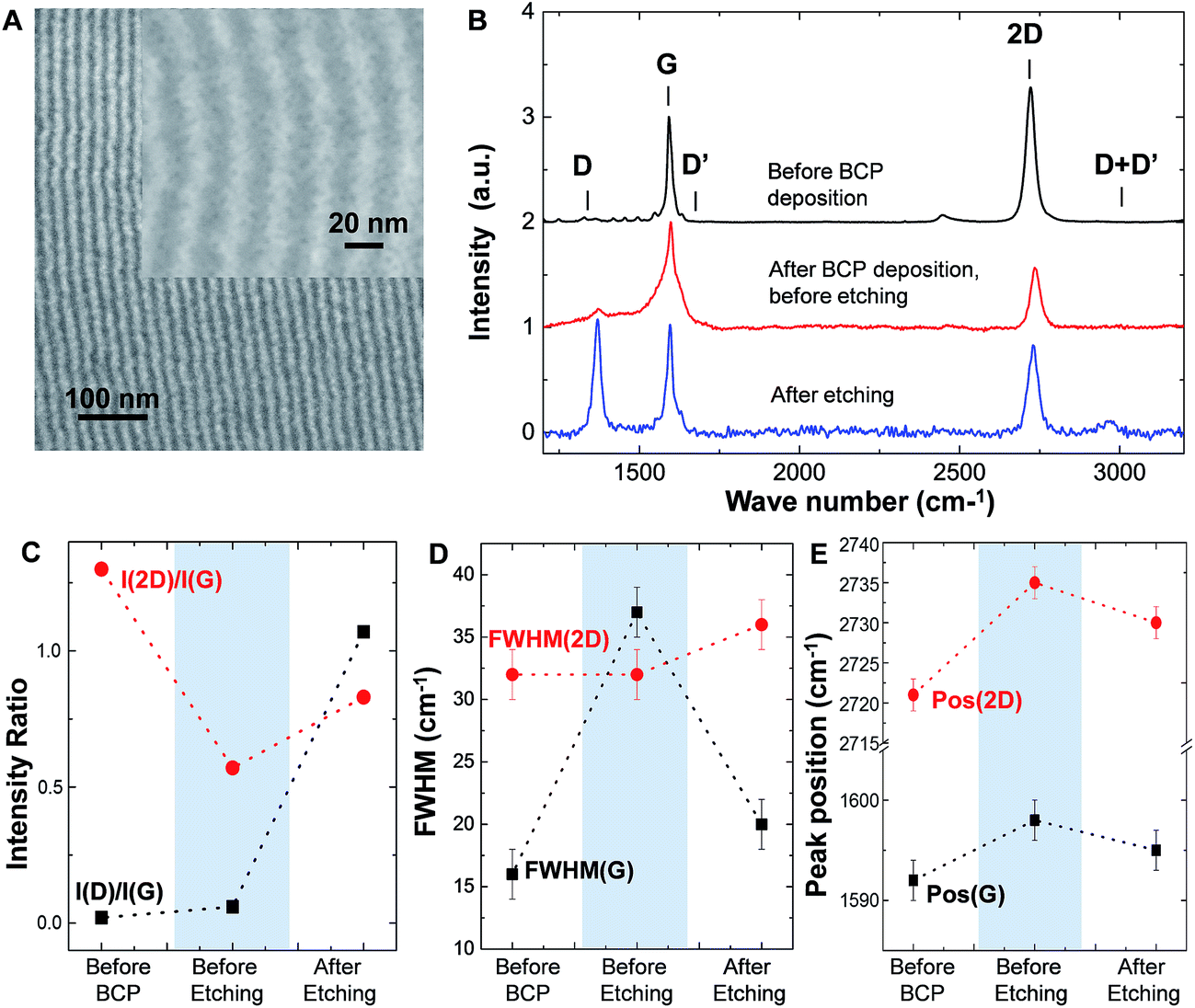 | ||
| Fig. 4 Raman analysis of nanopatterned graphene. (A) SEM image of an array of GNR after PS and graphene etch. Inset shows high magnification of GNR with ∼8 ± 2 nm ribbon width; confinement of GNR between SU-8 trenches are shown in ESI Fig. SI.1.† The spatial homogeneity of ribbons was proved by Raman maps of I(G) and I(D) as shown in Fig. SI.2.† (B) Raman spectra of graphene before BCP deposition, after BCP deposition and after PS and graphene etch. (C) Evolution of I(D)/I(G) ratio (black) and I(2D)/I(G) intensity ratio (red) during the fabrication of BCP graphene nanoribbons. (D) Evolution of FWHM (G) (black) signal together with FWHM(2D) (red) during the fabrication of BCP graphene nanoribbons. (E) Shifts in the G (black) and 2D (red) peak positions during the fabrication process. | ||
Oxygen based plasma removes PS and graphene, while the oxidized PDMS remains on top of the graphene nanoribbons. Fig. 4B shows the Raman spectra of the graphene before processing (black) and the evolution after the two main steps of the process: BCP deposition, before etching (red) and after etching (blue). Initially, the graphene used in this study showed residual D and D′ peaks (I(D)/I(G) ∼ 0.02). Such disorder may occur during the CVD growth process and/or transfer to SiO2 substrates, as reported.29 We also note that the graphene is doped since the position of the G peak (Pos(G)) is upshifted with respect to the value of pristine graphene (∼1585 cm−1).30 The spinning and growing of the BCP films on the graphene increases the I(D)/I(G) ratio to 0.06 (Fig. 3C). At a first glance, the increase of I(D)/I(G) could be attributed to the introduction of a slight amount of disorder in the monolayer occurring during the polymer deposition. However, the sudden increase of the full width half maximum of the G peak, FWHM(G) (Fig. 4B and D), from 16 to 38 cm−1 and the absence of any change in the full width half maximum of the 2D peak (FWHM(2D)) does not support the formation of point defects in graphene at this stage. This type of disorder would cause a comparable increment of both FWHM(G) and FWHM(2D),31 which is not the case here. Instead, the observed changes of the I(D)/I(G) ratio, FWHM(G) and FWHM(2D) could be explained due to the existence of amorphous carbon (αC) deposited on top of graphene;32 or more realistically, it could be an artifact coming from the presence of the PS polymer on top of graphene. The latter is supported by the fact that PS has to peaks close to the G peak at 1592 cm−1 and 1613 cm−1, respectively.33
In addition, the increase in peak position of the G (Pos(G)) and 2D (Pos(2D)) peaks (Fig. 3E) indicate that the polymer layer introduces p doping in the graphene sheet.30 This evidence is corroborated with a considerable decrease of the I(2D)/I(G) ratio30 from 1.3 to 0.57 (Fig. 4C).
After the PS etching with O2 plasma, we observe a significant increase of the I(D)/I(G) ratio to 1.07, a slight increment of the D′ peak with respect to the initial graphene and the appearance of a small D + D′ peak. The I(D)/I(G) increment is consistent with the actual creation of the graphene nanoribbon, discarding the major creation of additional random point defects in the monolayer during the lithographic process. This minimal presence of defects is supported by the increase of the ratio I(2D)/I(G) from 0.57 to 0.83 (Fig. 4C). Disorder should lead to a decrease of the I(2D)/I(G) ratio,31 but in this case it increases due to the decrement in doping of the final graphene ribbons.30 Also, the FWHM(2D) increases only slightly by 3 cm−1 with respect to the previous stages. In general, FWHM(2D) remains constant for changes in doping level and increases only with disorder.31 These trends show that the insertion of disorder in the process is moderated and is most likely to be introduced only near the ribbon edge, where the PDMS masking is least efficient.
Finally, it is interesting to point out that etching lead to a decrease of the FWHM(G). This can be understood just by noting that the PS areas are completely removed after the etching process, thus, confirming that the solely increment of FWHM(G) in the Raman spectra at the previous stage (polymers on top of graphene) was indeed an artifact due to the presence of PS.
In comparison with the graphene before processing, both FWHM(G) and FWHM(2D) increased only slightly after etching (3–4 cm−1), which supports the notion of disorder mainly at the edge of the ribbons and not in the channel. Since in our present study the oxidized PDMS is left on top of graphene nanoribbons we comment about its final influence in the nanoribbons. From the initial pristine graphene layer, we have an overall shift from 1592 cm−1 to 1596 cm−1 for Pos(G) and from 2721 cm−1 to 2730 cm−1 in the case of Pos(2D). Knowing that FWHM(G) is kept below 20 cm−1 during the entire process, the introduced disorder is low, mainly located at the ribbon edge, and we can ascribe these peak shifts uniquely to PDMS doping.34 Thus, we observe that PDMS introduces of hole-dopants in the monolayer35,36 and its density can be estimated to be ∼5 × 1012 cm−2;30,35,37 a doping value which is ∼50% larger than the initial doping value (∼1 × 1013 cm−2).30,37,38 We note that the removal of the oxidized PDMS could be done with HF, however, for clarity we leave this task out of the present work.
In order to quantify the amount of disorder introduced in the etching process, we analyze the obtained Raman spectra accounting for the two different types of defects that may be present in the system. First, the patterning itself could introduce a characteristic crystallite length scale related to the boundaries of the GNR, and second, point defects may occur within the ribbon (not only in the channel but also at the edge) if the PDMS mask is invasive (i.e. it damages graphene) or fails in providing complete protection during the etching step.35
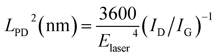
The disorder in a nano-crystallite can be quantified by the amount of boundaries with respect to the crystallite area, which is a measure of the inverse nano-crystallite size 1/LNC.32–38 Meanwhile, disorder generated by point defects is better quantified by the point-like defect concentration, given by (1/LPD2), where LPD is the average inter-defect distance.35 For our analysis, we use the Tuinstra–Koenig relation to obtain LNC and a modified version of this relation32–38 to extract LPD (the latter is valid in the case of low defect density, i.e. LPD > 6 nm):
| LNC (nm) = (2.4 × 10⁻¹⁰)λlaser4(ID/IG)−1 | (1) |
 | (2) |
Supposing that the disorder originates from ‘clean’ graphene boundaries, eqn (1) estimates a ribbon channel (LNC) of 9.6 nm, perfectly agreeing with the 8–10 nm width as shown in inset in Fig. 4A. The entire activation of the D band measured in BCP graphene nanoribbons would be, thus, fully accounted for by the ribbon edges. Nevertheless, we need to take into account the other extreme case, the full activation of the D band through point defects; since the possibility of achieving a perfectly clean graphene boundary from a plasma etch process is remote. From eqn (2), the interdefect distance LPD is 7.8 nm, matching again with the width of the nanoribbon. This fact indicates that the contribution of point defects in the graphene ribbons is residual and probably located close to the edges, where the PDMS masking is least efficient.
In order to inspect the homogeneity of the ribbon width, we performed a Raman map of a 8 μm × 8 μm area (Fig. SI. 2†). Clearly, I(D) and I(G) show similar values over the entire mapped area, proving the homogeneity of the above estimated ribbon channel (I(D)/I(G) ∼ 1).
Next, we compare the quality of the here presented BCP graphene nanoribbons with respect to other fabrication procedures reported in literature.16,27 As quantified above through the I(D)/I(G) ratio, the presence of point defect in BCP graphene ribbons is residual, which is corroborated with a I(2D)/I(G) ratio of 0.83 (despite the presence of doping), an almost non-existent D + D′ peak and a FWHM(2D) close to the one of pristine graphene (33 cm−1).39 Meanwhile, other top-down techniques such as EBL patterned graphene using HSQ exhibit larger feature sizes with respect to the BCP nano-patterning technique used in our work, together with a considerable amount of amorphization within the graphene ribbon.16 In addition, the combined technique composed of EBL lithography and a gas-phase chemical narrowing,27 produces similar feature sizes to our BCP case. These latter ribbons are, however, almost fully amorphous as demonstrated by the absence of a clear 2D peak.27
Being a top-down approach, the technique presented here produces similar ribbon quality to bottom-up alternatives, such as multilayer graphene ribbons created by unzipping carbon nanotubes,40–43 although the latter are not scalable alternatives. We also note that although being within the state of the art in terms of feature size and demonstrating a high integrity of the ribbons, this type of fabrication method is unable to select the edge chirality of the ribbon as recently reported in 40 nm wide graphene ribbons on SiC.44
Experimental
On-chip BCP mask development and pattern transfer
Silicon substrates as received within clean room environment and with no prior surface treatment or cleaning were cut into 2.0 cm2 pieces. PS-b-PDMS (5k–5.5k) block copolymer thin films were spin cast from a 1 wt% toluene solution at 3200 rpm for 30 s. The BCP films were initially solvo-thermal annealed at 22 °C (room temperature), 35 °C, 45 °C and 55 °C for 5 to 20 min under toluene vapours in a covered steel chamber mounted on a hot plate to control temperature via a thermocouple in the solvent reservoir. Once the optimal BCP annealing condition was obtained then it was investigated on topographically patterned Si and graphene substrates. After annealing at a given time all the samples were immediately removed from the chamber and left to cool and dry at ambient conditions.The solvo-thermal annealed PS-b-PDMS films were subjected to selective PS etch using O2 plasma for 10 s with 2000 W power in ICP and 400 W power in RIE at 2.0 Pa pressure. SF6 and CF4 plasma at 70 sccm and 35 sccm flow rate with ICP (inductively coupled plasma) and RIE (reactive ion etching) powers of 1200 W and 200 W at 1.9 Pa pressure was used to etch silicon. Oxygen plasma at RIE was used to subsequently etch PS and graphene for 20 s with RIE power of 200 W.
Scanning electron microscopy
Top-down SEM images of BCP, oxidised PDMS, oxidised PDMS on top of nanopatterned graphene and silicon nanofeatures were obtained by using a Field Emission Zeiss Ultra Plus scanning electron microscope with a Gemini column operating at an accelerating voltage of 3 kV. Unless otherwise stated, all the shown SEM images were taken after PS removal by O2 plasma and consequential oxidation of PDMS.Raman analysis
Raman spectra were measured using a DXR Raman Microscope from Thermo Scientific equipped with a 100× objective. The excitation wavelength of the laser was 455 nm. The laser power was below 1 mW to avoid sample heating and the acquisition time was of the order of a few minutes. The experimental resolution of the apparatus is ∼2 cm−1. The calibration was carried out by checking Rayleigh band and Si band at 0 cm−1 and 521 cm−1, respectively. Raman peaks from 3 individual samples were fitted with a single symmetrical Lorentzian function to extract the corresponding experimental parameters. The spectra were treated with a statistical analysis, in order to minimize the error in the measurements.Conclusion
In summary, we have demonstrated highly ordered line patterns formed by self-assembly of lamellar PS-b-PDMS (5k–5.5k) without any surface treatment on both silicon and graphene substrates. Topographically pre-patterned substrates allow for predictable structure alignment and controlled number of lines of oxidized PDMS in each trench, from 9 lines inside 200 nm tranches to a single line inside 30 nm trenches. This rapid brushless on-chip mask template was used for direct patterning of graphene to get sub-10 nm GNRs. Raman analysis not only shows that the buried graphene is indeed nanopatterned, but also that the disorder is mainly arising from the lithographic edges rather than point defects in the channel. The realization of nanoribbons free of disorder in the channel is one of the crucial conditions for such structures to exhibit energy band gaps or ballistic transport, as predicted in theoretical studies.11Acknowledgements
Financial support for this work is provided by The Center for Nanostructured Graphene sponsored by the Danish National Research Foundation, Project DNRF58, by the EU FP7 NMP project, LAMAND (grant number 245565) project and by the Science Foundation Ireland (grant number 09/IN.1/602). J.M.C and P.B. acknowledge financial support from the EC Graphene FET Flagship.References
- G. E. Moore, Proc. IEEE, 1998, 86, 82–85 CrossRef.
- C. A. Mack, IEEE Trans. Semicond. Manuf., 2011, 24, 202–207 CrossRef.
- M. M. Salour, M. Batayneh and L. Figueroa, Appl. Phys. A: Mater. Sci. Process., 2011, 105, 289–300 CrossRef CAS.
- D. Borah, M. T. Shaw, S. Rasappa, R. A. Farrell, C. O'Mahony, C. M. Faulkner, M. Bosea, P. Gleeson, J. D. Holmes and M. A. Morris, J. Phys. D: Appl. Phys., 2011, 44, 174012–174024 CrossRef.
- H.-P. Cong, J.-F. Chen and S.-H. Yu, Chem. Soc. Rev., 2014, 43, 7295–7325 RSC.
- K. S. Novoselov, A. K. Geim, S. V. Morozov, D. Jiang, M. I. Katsnelson, I. V. Grigorieva, S. V. Dubonos and A. A. Firsov, Nature, 2005, 438, 197–200 CrossRef CAS PubMed.
- P. L. Neumann, E. Tovari, S. Csonka, K. Kamaras, Z. E. Horvath and L. P. Biro, Nucl. Instrum. Methods Phys. Res., Sect. B, 2012, 282, 130–133 CrossRef CAS PubMed.
- M. Y. Han, B. Oezyilmaz, Y. Zhang and P. Kim, Phys. Rev. Lett., 2007, 98, 206805–206809 CrossRef.
- B. Oezyilmaz, P. Jarillo-Herrero, D. Efetov and P. Kim, Appl. Phys. Lett., 2007, 91, 192107–192110 CrossRef PubMed.
- T. G. Pedersen, C. Flindt, J. Pedersen, N. A. Mortensen, A.-P. Jauho and K. Pedersen, Phys. Rev. Lett., 2008, 100, 136804 CrossRef.
- N. M. R. Peres, A. H. Castro Neto and F. Guinea, Phys. Rev. B: Condens. Matter Mater. Phys., 2006, 73, 125411–125434 CrossRef.
- X. Li, X. Wang, L. Zhang, S. Lee and H. Dai, Science, 2008, 319, 1229–1232 CrossRef CAS PubMed.
- X. Liang, Y.-S. Jung, S. Wu, A. Ismach, D. L. Olynick, S. Cabrini and J. Bokor, Nano Lett., 2010, 10, 2454–2460 CrossRef CAS PubMed.
- J. G. Son, M. Son, K.-J. Moon, B. H. Lee, J.-M. Myoung, M. S. Strano, M.-H. Ham and C. A. Ross, Adv. Mater., 2013, 25, 4723–4728 CrossRef CAS PubMed.
- M. Y. Han, J. C. Brant and P. Kim, Phys. Rev. Lett., 2010, 104, 056801 CrossRef.
- S. Ryu, J. Maultzsch, M. Y. Han, P. Kim and L. E. Brus, ACS Nano, 2011, 5, 4123–4130 CrossRef CAS PubMed.
- Q. Yu, L. A. Jauregui, W. Wu, R. Colby, J. Tian, Z. Su, H. Cao, Z. Liu, D. Pandey, D. Wei, T. F. Chung, P. Peng, N. P. Guisinger, E. A. Stach, J. Bao, S.-S. Pei and Y. P. Chen, Nat. Mater., 2011, 10, 443–449 CrossRef CAS PubMed.
- S. O. Kim, H. H. Solak, M. P. Stoykovich, N. J. Ferrier, J. J. de Pablo and P. F. Nealey, Nature, 2003, 424, 411–414 CrossRef CAS PubMed.
- S. Rasappa and S. Rasappa, Block copolymer self-assembly based device structures, 2013 Search PubMed.
- S. Rasappa, D. Borah, R. Senthamaraikannan, C. C. Faulkner, M. T. Shaw, P. Gleeson, J. D. Holmes and M. A. Morris, Thin Solid Films, 2012, 522, 318–323 CrossRef CAS PubMed.
- C. Girardot, S. Böhme, S. Archambault, M. Salaün, E. Latu-Romain, G. Cunge, O. Joubert and M. Zelsmann, ACS Appl. Mater. Interfaces, 2014, 6, 16276–16282 CAS.
- J. G. Son, K. W. Gotrik and C. A. Ross, ACS Macro Lett., 2012, 1, 1279–1284 CrossRef CAS.
- E. Kim, W. Kim, K. H. Lee, C. A. Ross and J. G. Son, Adv. Funct. Mater., 2014, 24, 6981–6988 CrossRef CAS PubMed.
- D. Borah, S. Rasappa, R. Senthamaraikannan, J. D. Holmes and M. A. Morris, Langmuir, 2013, 29, 8959–8968 CrossRef CAS PubMed.
- S. Rasappa, L. Schulte, D. Borah, M. A. Morris and S. Ndoni, J. Colloid Interface Sci., 2014, 2, 1–5 CrossRef PubMed.
- S. Park, J. M. Yun, U. N. Maiti, H.-S. Moon, H. M. Jin and S. O. Kim, Nanotechnology, 2014, 25, 014008–014014 CrossRef PubMed.
- X. Wang and H. Dai, Nat. Chem., 2010, 2, 661–665 CrossRef CAS PubMed.
- C. A. Ross, Y. S. Jung, V. P. Chuang, J. G. Son, K. W. Gotrik, R. A. Mickiewicz, J. K. W. Yang, J. B. Chang, K. K. Berggren, J. Gwyther and I. Manners, Alternative Lithographic Technologies Ii, 2010, p. 7637 Search PubMed.
- A. Dimiev, D. V. Kosynkin, A. Sinitskii, A. Slesarev, Z. Sun and J. M. Tour, Science, 2011, 331, 1168–1172 CrossRef CAS PubMed.
- A. Das, S. Pisana, B. Chakraborty, S. Piscanec, S. K. Saha, U. V. Waghmare, K. S. Novoselov, H. R. Krishnamurthy, A. K. Geim, A. C. Ferrari and A. K. Sood, Nat. Nanotechnol., 2008, 3, 210–215 CrossRef CAS PubMed.
- I. Childres, L. A. Jauregui, J. Tian and Y. P. Chen, New J. Phys., 2011, 13, 025008–025020 CrossRef.
- J. Hong, M. K. Park, E. J. Lee, D. Lee, D. S. Hwang and S. Ryu, Sci. Rep., 2013, 3, 2700 Search PubMed.
- A. Palm, J. Phys. Chem., 1951, 55, 1320–1324 CrossRef CAS.
- C. C, asiraghi, Phys. Status Solidi RRL, 2009, 3, 175–177 CrossRef PubMed.
- S. Mikhailov, Physics and Applications of Graphene - Experiments, InTech Publishers, 2011 Search PubMed.
- S. Winters, T. Hallam, H. Nolan and G. S. Deeberg, Phys. Status Solidi B, 2012, 249, 2515–2518 CrossRef CAS PubMed.
- J. M. Caridad, F. Rossella, V. Bellani, M. Maicas, M. Patrini and E. Diez, J. Appl. Phys., 2010, 108, 084321–084327 CrossRef PubMed.
- A. C. Ferrari and J. Robertson, Phys. Rev. B: Condens. Matter Mater. Phys., 2000, 61, 14095–14107 CrossRef CAS.
- L. G. Cancado, K. Takai, T. Enoki, M. Endo, Y. A. Kim, H. Mizusaki, A. Jorio, L. N. Coelho, R. Magalhaes-Paniago and M. A. Pimenta, Appl. Phys. Lett., 2006, 88, 163106–163109 CrossRef PubMed.
- A. C. Ferrari and D. M. Basko, Nat. Nanotechnol., 2013, 8, 235–246 CrossRef CAS PubMed.
- C. Stampfer, F. Molitor, D. Graf, K. Ensslin, A. Jungen, C. Hierold and L. Wirtz, Appl. Phys. Lett., 2007, 91, 241907–241910 CrossRef PubMed.
- L. Jiao, X. Wang, G. Diankov, H. Wang and H. Dai, Nat. Nanotechnol., 2010, 5, 321–325 CrossRef CAS PubMed.
- L. Xie, H. Wang, C. Jin, X. Wang, L. Jiao, K. Suenaga and H. Dai, J. Am. Chem. Soc., 2011, 133, 10394–10397 CrossRef CAS PubMed.
- J. Baringhaus, M. Ruan, F. Edler, A. Tejeda, M. Sicot, A. Taleb-Ibrahimi, A.-P. Li, Z. Jiang, E. H. Conrad, C. Berger, C. Tegenkamp and W. A. de Heer, Nature, 2014, 506, 349–354 CrossRef CAS PubMed.
Footnote |
| † Electronic supplementary information (ESI) available. See DOI: 10.1039/c5ra11735f |
| This journal is © The Royal Society of Chemistry 2015 |