DOI:
10.1039/C5RA12332A
(Paper)
RSC Adv., 2015,
5, 66403-66408
Ultra-long SiC nanowires synthesized by a simple method
Received
25th June 2015
, Accepted 28th July 2015
First published on 28th July 2015
Abstract
Ultra-long SiC nanowires with lengths ranging from several millimeters to one centimeter were successfully prepared from graphite, silicon, silica and alumina raw materials via a simple carbon thermal reduction method in a tube furnace at 1300 °C. Scanning electron microscopy (SEM), electron energy scattering (EDX), X-ray diffraction (XRD), transmission electron microscopy (TEM), high-resolution transmission electron microscopy (HRTEM) and Fourier transform infrared spectroscopy (FTIR) were employed to characterize the morphology and microstructure of the obtained products. The results showed that the nanowires mostly consisted of 3C–SiC and exhibited mainly a straight-line shape with diameters in the range of 30–150 nm. Alumina may be a novel and highly effective mediator playing an important role in controlling the concentration of SiO during the growth of ultra-long SiC nanowires and an alumina-assisted growth of the vapor–solid (VS) mechanism was proposed for the growth mode of ultra-long SiC nanowires.
1. Introduction
Since the discovery of carbon nanotubes by Iijima in 1991,1 one-dimensional (1-D) nanomaterials have attracted wide attention because of their unique microstructures, properties and great potential applications.2–5 1-D SiC nanomaterials, most commonly in the 1-D nanomaterials, not only inherit the outstanding properties from bulk counterparts, such as thermostability, anti-oxidation, corrosion resistance and high hardness,6–8 but also have unique properties, including superior mechanical properties, excellent field emission properties and special photoluminescence properties due to their unique morphology.9–11 These properties make them have broad applications in the fields of high-temperature structural materials, micro- and nano- electronics, catalysis, etc.12–15 SiC nanowires have been synthesized by several techniques, such as the laser ablation, arc-discharge, thermal evaporation, chemical vapor deposition, carbon thermal reduction, and so on.16–19 However, the lengths of SiC nanowires are mostly in a range of several to several hundred micrometers limiting their further research and application based on the above methods. To date, the synthesis of ultra-long SiC nanowires with the lengths on the order of millimeters or even centimeters was seldom reported according to our survey. In 2009, Li Gongyi et al. obtained large areas of millimeters long β-SiC nanowires with the organics powder of polycarbosilane, which is very expensive and sometimes emits toxic reagents, in a polymer pyrolysis CVD route.20 Lin Liangwu synthesized several centimeters ultra-long SiC nanowires using the organic gas of CH4 as the carbon source and SiO or the mixture of Si and SiO2 as the silicon source by a catalyst-free CVD route under superatmospheric pressure conditions in 2011.21 In addition, the required superatmospheric pressure is important for the synthesis of ultra-long β-SiC nanowires, which can easily adjust the pressure of the vapors to supersaturation condition.21,22 As we all known, the mixture of this approach is flammable due to the presence of organic gas of CH4 and the superatmospheric pressure condition requires special laboratory equipments. Although ultra-long SiC nanowires can be produced by the above two ways, both of them are involved the organic compounds and the demands of materials, equipments and processes are very severe. It is still necessary to develop a simpler and more effective method to prepare ultra-long SiC nanowires. Moreover, although intensive efforts have been made on understanding the mechanism of SiC nanowires, such as VS growth mechanism, vapor–liquid–solid (VLS) growth mechanism, solid–liquid–solid (SLS) growth mechanism and oxide assisted growth (OAG), further work in the perspective of understanding the growth process of SiC nanowires is still required.
In this paper, ultra-long 3C–SiC nanowires with the lengths from several millimeters to one centimeter were successfully fabricated by using the inexpensive inorganic powders, including graphite, silicon, silica and alumina, as raw materials via a simple carbon thermal reduction method. Compared with the synthesis of ultra-long SiC nanowires reported above, the process in our experiment exhibits inherent benefits, including inexpensive raw materials, the simplicity of the procedures, the low requirement of equipments and the condition of atmospheric-pressure. In addition, the role of alumina was investigated, which was rarely reported, during the growth of SiC nanowires according to our previous survey. Furthermore, a possible growth mechanism for the as-grown ultra-long 3C–SiC nanowires was also proposed. This simple method provides an effective means of fabricating ultra-long SiC nanowires on an industrial scale.
2. Experimental
Silicon (100 nm, purity 99.9%), silica (15 nm, purity 99.9%), graphite powders (5 μm, purity 99.8%) and alumina (purity 99%) were used as the raw materials. The powder was mixed as follows: 33–43 wt% graphite (G), 17–19 wt% Si, 35–42 wt% SiO2 and 5–6 wt% Al2O3. The mixture powder was ball-milled in ethanol for 10 h with SiC balls and then dried in a rotating evaporator. Activated carbon (AC) powders were first ultrasonically washed in ethanol and then dried naturally. A ceramic crucible (60 mm × 30 mm × 30 mm) was used to hold the mixture powder (1 g), whose surface was covered with the dried activated carbon powder (2 g). The crucible was placed into a tube corundum furnace. Before heating, the argon gas (99.999%) was introduced into the furnace at a rate of 300 ml min−1 for ten minutes and then changed the flowing speed to 100 ml min−1 under atmospheric-pressure. The furnace was heated up at 10 °C min−1 from room temperature to 900 °C and maintained for 2 h, and then further heated up to 1300 °C at a speed of 5 °C min−1 and maintained for 2 h. High-purity argon gas was keep flowing during the experimental process. After the heating was terminated, the furnace was first cooled to 800 °C at a speed of 5 °C min−1 and then naturally cooled to room temperature. The final products looked like white wools were found on the inner wall of the crucible and on the surface of the mixture powder.
The as-obtained products were analyzed by scanning electron microscopy (SEM, HELIOS NanoLab 600i, America) equipped with energy dispersive spectroscopy (EDX) to observe the morphology and analyze the elemental composition. X-ray powder diffraction (XRD, X'PERT PRO MPD, Holland), transmission electron microscopy and high-resolution transmission electron microscopy (TEM and HRTEM, Tecnai G2-F30, America) were used to identify the crystalline phase and the microstructure of the samples, respectively. Samples for TEM and HRTEM observation were dispersed in ethanol by ultrasonication for 20 min, and a drop of the suspension containing the products was dripped onto a copper grid coated with an amorphous carbon supporting film and then dried in air. Fourier transform infrared spectroscopy (FTIR, Spectrum Two, America) was also conducted to confirm the composition of the product.
3. Results and discussion
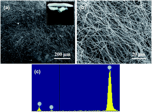
The morphology of the white cotton-like products was characterized by SEM firstly. Fig. 1 show SEM images and EDX spectrum of the white cotton-like products prepared at 1300 °C incubated for 2 h. The SEM images at low-magnification (Fig. 1a) and high-magnification (Fig. 1b) both revealed that the white cotton-like products are both straight and curved nanowires grown randomly. From the low-magnification SEM image and macroscopic morphology of the achieved cotton-like products shown in Fig. 1a, it can be seen that the lengths of nanowires are from hundreds to thousands of micrometers. The high-magnification SEM image (Fig. 1b) of nanowires suggests that the nanowires have a smooth surface, but the diameters of nanowires are fluctuating from 30 nm to 150 nm. No catalytic nanoparticles are found at the tips of the grown nanowires indicating that the VLS mechanism is not responsible for nanowire growth.20,22,23 The compositions of the nanowires were measured by EDX under high resolution SEM and a typical EDX spectrum obtained from the stem of the nanowire is shown in Fig. 1c. We can see that the stem of the nanowire is composed of Si, C and little amount of O. So we roughly infer that the nanowires are the composite of SiC and SiOx.
 |
| | Fig. 1 SEM images and EDX spectrum of SiC nanowires formed by annealing at 1300 °C for 2 h in the ceramic crucible. SEM images collected from (a) low-magnification and (b) high-magnification and macroscopic morphology of the achieved cotton-like products. (c) EDX spectrum obtained from the stem of nanowires. | |
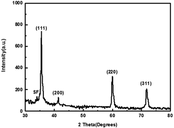
The crystalline phase of the products was characterized by XRD shown in Fig. 2. In the XRD pattern, the four major intensities peaks are assigned to the (111), (200), (220), and (311), which are reflections of cubic 3C–SiC. The lattice parameter calculated from the XRD data is in good agreement with that of the known value. In addition, the 3C–SiC diffraction peaks are obviously broadened, which may be the results of the effect of nanosize and surface states.24 The peak marked with SF is attributed to stacking faults similar to those previously reported.25,26 Meanwhile, the intensity ratio of 2θ = 33.6° and 2θ = 41.4° (I33.6°/I41.4°) can be used to evaluate the relative content of stacking faults in the whiskers as reported in other literature.27 The XRD data exhibits that the intensities of 2θ = 33.6° and 2θ = 41.4° are 108 and 130, respectively. The ratio of the two intensities is low than 1 suggesting that SiC nanowires contain low densities of stacking faults compared with the previous reports.27,28
 |
| | Fig. 2 Typical XRD pattern of the synthesized products obtained by annealing at 1300 °C for 2 h. | |
The morphology and composition of SiC nanowires were further investigated by TEM and HRTEM. From the typical TEM image of SiC nanowires as shown in inset of Fig. 3, it can be seen that SiC nanowire has a smooth surface with a diameter of 30–40 nm. Due to no droplets found at the tips of SiC nanowires indicating that the growth mechanism is more reasonable attributed to a VS mechanism rather than a VLS mechanism as reported in many other literature.20,22,23 From the typical HRTEM image in Fig. 3, it can be noticed that SiC nanowire consists of a crystalline core coated with a thin amorphous shell layer (3–4 nm thickness). There are some stacking faults and twins along the growth direction of SiC nanowire. The insert in Fig. 3 shows that the inter-planar spacing perpendicular to SiC nanowire axes is about 0.25 nm, which is consistent with the (111) plane space of 3C–SiC, suggesting that the growth direction of SiC nanowire is along [111].23,29,30 To further study the structure, FTIR measurement was performed for the obtained ultra-long SiC nanowires and a typical FTIR transmittance spectrum is shown in Fig. 4. The strong absorption peak centered at 802 cm−1 can be attributed to the transverse optical (TO) photon vibration mode of the Si–C bonds.31,32 The absorption peaks at 482 and 1083 cm−1 are belonging to the Si–O–Si and Si–O stretching vibrations, respectively.33,34 Combined with the FTIR spectrum (Fig. 4), EDX spectrum (Fig. 1c), XRD pattern (Fig. 2) and HRTEM observation (Fig. 3), it is believed that the core of obtained nanowires is crystalline SiC and that the shell is a very thin amorphous SiOx layer.35
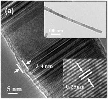 |
| | Fig. 3 Typical TEM and HRTEM images of SiC nanowires obtained by the materials of graphite, silicon, and silicon dioxide with the assistance of alumina via annealing at 1300 °C for 2 h. | |
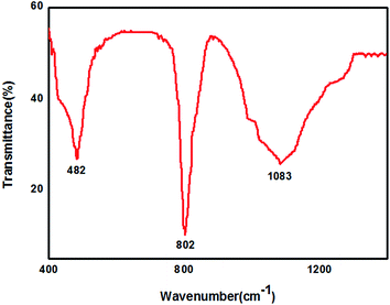 |
| | Fig. 4 Typical FTIR transmittance spectrum of the ultra-long SiC nanowires obtained at 1300 °C for 2 h. | |
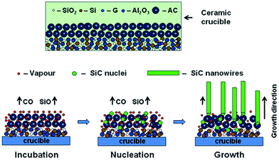
To explain the growth mechanism of SiC nanowires, many models were proposed, such as VS, VLS, SLS and OAG. In the typical VLS and SLS growth process, the metal particle acted as a nucleation active site should be located at the tip of the nanowire. However, no metal particles were observed at the tips of SiC nanowires in our experiment suggesting that the VLS and SLS mechanisms are not suitable for disclosing the growth process of as-prepared SiC nanowires. To understand the growth mechanism of the obtained nanowires, a comparison experiment was carried out without employed alumina, while other experimental parameters were kept constant. The as-obtained products are low-yield but tens to hundreds of micrometers nanowires as shown in Fig. 5. According to the experimental phenomena, alumina is critical for the growth of ultra-long SiC nanowires, while it cannot be used as a catalyst due to a high melting point. Based on the physical and chemical properties, we tend to propose the following reasons to elaborate the effect of alumina on the growth process of SiC nanowires. First, according to the previous literature,36 Al2O3 can react with SiO2 as shown in reaction (1) and prohibit the formation amount of SiC. However, the production of reaction (1), namely mullite is a metastable phase when the temperature and the mole fractions of SiO2 and Al2O3 are within a certain range based on the result of the literature.37,38 Furthermore, the metastable phase can take place the liquid phase separation process and generate SiO2 in a liquid phase,37,38 and then promote the reaction (2) to produce SiO which is an important reactant gas for SiC nanowires mainly driven by the concentration grads. Secondly, the liquid phase formation temperature of Al2O3–SiO2 will be significantly decreased when a small amount of impurity oxide is contained in the system of Al2O3–SiO2, such as the liquid phase formation temperature of Al2O3–SiO2 system with a low content of alumina is 1595 °C, while it will reduce to 985 °C when introducing 1% K2O to the system of Al2O3–SiO2 (–K2O) based on the literature.39 0.5–0.7% Na2O is contained in alumina and maybe similarly reduce the liquid phase formation temperature of Al2O3–SiO2 (–Na2O) system. What's more, the size effect on the liquid phase formation temperature is also should be taken into account. Therefore, the liquid phase separation process to generate SiO2 in a liquid phase can be more easily occurred and it is reasonable to believe that alumina can play an important role in adjusting the content of reactive SiO2 liquid and then continuously accommodating the concentration of SiO to promote the growth of SiC nanowires with the change of temperature. Combined with the role of alumina, we tend to propose an alumina-assisted VS mechanism to explain the growth of ultra-long SiC nanowires. Based on the experimental results, a possible growth process of SiC nanowires is illustrated with following as shown in Fig. 6 and the growth process is divided into three stages for discussion.
| | |
2SiO2 (s; l) + 3Al2O3 (s; l) → 3Al2O3·2SiO2 (s; l)
| (1) |
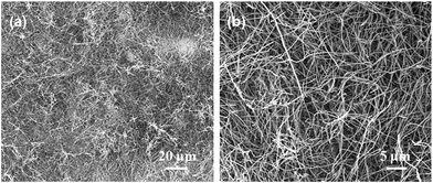 |
| | Fig. 5 SEM images of SiC nanowires without employed alumina as raw material collected from annealing at 1300 °C for 2 h in the ceramic crucible. | |
 |
| | Fig. 6 Illustrations of possible growth process of SiC nanowires. | |
The first stage is incubation to prepare for the post-nucleation. Following reactions may occur during this period:
| | |
2Si (s) + O2 (g) → 2SiO (g)
| (2) |
| | |
2C (s) + O2 (g) → 2CO (g)
| (3) |
| | |
SiO2 (s) + Si (s) → 2SiO (g)
| (4) |
| | |
SiO2 (s) + C (s) → SiO (g) + CO (g)
| (5) |
| | |
SiO2 (s) + CO (g) → SiO (g) + CO2 (g)
| (6) |
| | |
CO2 (g) + C (s) → 2CO (g)
| (7) |
Owing to the effect of size of the raw materials, the initial reaction temperature of the above reactions maybe drop.40,41 According to the thermodynamic data,42 the changes in Gibbs free energy of reactions (2) and (3) are very close and lower than zero at low temperature (below 900 K), while the changes in Gibbs free energy of other reactions are positive. Therefore, the reactions (2) and (3) can take place firstly and others cannot proceed spontaneously at low temperature from the view of thermodynamics. Meanwhile, the concentrations of SiO and CO are also very close due to the nearly changes in Gibbs free energy of reaction (2) and (3). It can be found that the reactions (2) and (3) all need oxygen, which may be derived from the following ways: (a) the oxidation of nano-powder at room temperature; (b) the oxidation of nano-powder during the ball-milling and drying; (c) the poor air tightness of experimental equipments. The minimum oxygen concentration, combined with the previous literature, required for the reactions is very low.43 Furthermore, SiO and CO gases, which are the reactants for SiC nucleation, can be easily generated during incubation and then SiC nucleation can be easily formed in the following stage.
The second stage is nucleation and the following reactions may take place to form SiC nuclei:
| | |
Si (s; l) + C (s) → SiC (s)
| (8) |
| | |
SiO (g) + 2C (s) → SiC (s) + CO (g)
| (9) |
| | |
SiO (g) + 3CO (g) → SiC (s) + 2CO2 (g)
| (10) |
| | |
3SiO (g) + CO (g) → SiC (s) + 2SiO2 (s)
| (11) |
According to the thermodynamic data, the changes in Gibbs free energy of above reactions (8)–(11) are all below zero suggesting that the above four reactions all can take place spontaneously from the thermodynamic point of view. However, the reactions (10) and (11) cannot proceed at low temperature due to the similar concentrations of SiO and CO. Therefore, owing to a lower the changes in Gibbs free energy compared with reaction (8), reaction (9) may be mainly responsible for the formation of SiC nuclei at first as well as providing the reactant gas CO for the subsequent reactions (10) and (11).44 Furthermore, the concentration of SiO will decrease and then reaction (10) may take place as well as providing the reactant gas CO2 for the subsequent reaction (7). The concentrations of SiO and CO are associated with the reactions happening and the above reactions (8)–(11) may take place to form SiC nuclei under the right conditions.
After the SiC nuclei formed, SiC nanowires may grow subsequently along a fixed axis. Therefore, the final stage is SiC nanowires subsequent growth along the axis direction. In general, the growth direction of SiC nanowires is preferentially normal to the lowest energy plane of β-SiC, which is the (111) plane from the crystallographic perspective. Furthermore, SiC nanowires will grow subsequently along a fixed direction as long as the reactant gases needed for the growth of SiC nanowires continuously generated. Meanwhile, owing to the participation of oxygen and the crystallographic mismatch caused by screw dislocations, SiC nanowires have a density of stacking faults, which has also been confirmed by the analysis of HRTEM.44,45 Moreover, the stacking faults are a typical characteristic for SiC nano-materials produced via solid–gas reaction of C and SiO as reported in other literature.22,46,47 According to this view, reaction (9) is firstly responsible for the growth of SiC nanowires and generates the CO vapor needed for the reactions (10) and (11). In the view of thermodynamic consideration, it should be noted that the reaction (11) can take place preferentially during the cooling stage.44 Therefore, owing to the lower melting point and slower solidification rate, SiO2 deposits on the surface of SiC and then a core–shell structure of SiC–SiO2 nanowires is formed.48 However, SiO2 can react with the evaporated gaseous containing silicon or carbon to obtain SiOx coated SiC nanowires when the amount of silicon or graphite is excess.
It is worth noting that the activated carbon played an important role in the growth of SiC nanowires. When activated carbon was not employed during the experiment, only a small amount of several millimeters SiC nanowires were obtained as shown in Fig. 7. These phenomena can be attributed to the strong adsorption of activated carbon due to the porous structures and large specific surface area. The gaseous reactants, such as SiO and CO, can be “held” by the pores of the activated carbon from diffusing quickly. Furthermore, local gas supersaturation can be easily reached, which is in favor of the subsequent growth of SiC nanowires.49
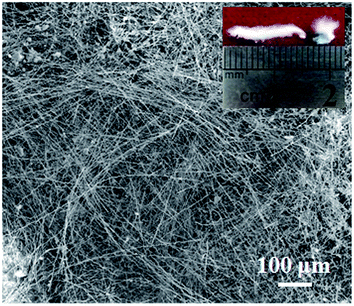 |
| | Fig. 7 SEM image and macroscopic morphology of the obtained cotton-like products without employed activated carbon. | |
It should also be pointed out that the exact growth mechanism of the ultra-long SiC nanowires and the exact role of alumina are still unclear and further work on the exact growth process is needed for a full understanding.
4. Conclusions
Ultra-long SiC nanowires have been successfully synthesized with the raw materials of graphite, silicon, silica and alumina by a simple carbon thermal reduction route under atmospheric-pressure conditions. SiC nanowires have a smooth surface with a diameter in the range of 30–150 nm and consist of a crystalline SiC covered by a thin layer of amorphous SiOx. The experimental results suggest that the growth of ultra-long 3C–SiC nanowires is probably dominated by the alumina-assisted VS mechanism and alumina may be as a novel and highly effective mediator playing an important role in controlling the concentration of SiO. The growth process can be divided into three stages, namely the incubation, nucleation and subsequent growth. This simple method offers great potential for industrial fabrication of ultra-long SiC nanowires.
Acknowledgements
This work was supported by the National Science Foundation (51202048, 11402252, 11421091 and 91216301) of China.
References
- S. Iijima, Nature, 1991, 354, 56–58 CrossRef CAS PubMed
 .
. - W. S. Shi, Y. F. Zheng, N. Wang, C. S. Lee and S. T. Lee, Adv. Mater., 2001, 13, 591–594 CrossRef CAS
 .
. - X. Duan, Y. Huang, R. Agarwal and C. M. Lieber, Nature, 2003, 421, 241–245 CrossRef CAS PubMed
 .
. - Y. Li, P. S. Dorozhkin, Y. Bando and D. Golberg, Adv. Mater., 2005, 17, 545–549 CrossRef CAS PubMed
 .
. - Y. Tian, H. W. Zheng, X. Y. Liu, S. J. Li, Y. J. Zhang, J. F. Hu and W. F. Zhang, Mater. Lett., 2012, 76, 219–221 CrossRef CAS PubMed
 .
. - C. Gaberstroh, R. Helbig and R. A. Stein, J. Appl. Phys., 1994, 76, 509–513 CrossRef PubMed
 .
. - J. B. Casady and R. W. Johnson, Solid-State Electron., 1996, 39, 1409–1422 CrossRef
 .
. - J. J. Chen, Y. Pan and R. B. Wu, Rare Met. Mater. Eng., 2010, 39, 90–94 Search PubMed
 .
. - H. Dai, E. W. Wong, Y. Z. Lu, S. Fan and C. M. Lieber, Nature., 1995, 375, 769–772 CrossRef CAS PubMed
 .
. - E. W. Wong, P. E. Sheehan and C. M. Lieber, Science., 1997, 277, 1971–1975 CrossRef CAS
 .
. - Z. Pan, H. L. Lai, F. C. Au, X. Duan, W. Zhou, W. Shi and S. S. Xie, Adv. Mater., 2000, 12, 1186–1190 CrossRef CAS
 .
. - A. H. Carim, K. K. Lew and J. Redwing, Adv. Mater., 2001, 13, 1489–1491 CrossRef CAS
 .
. - C. O. Jang, T. H. Kim, S. Y. Lee, D. J. Kim and S. K. Lee, Nanotechnology, 2008, 19, 345203 CrossRef PubMed
 .
. - W. Feng, J. T. Ma and W. Y. Yang, CrystEngComm, 2012, 14, 1210–1212 RSC
 .
. - H. J. Hwang, K. J. Lee, Y. T. An, B. H. Choi and W. S. Seo, Mater. Chem. Phys., 2012, 134, 13–15 CrossRef CAS PubMed
 .
. - M. Yudasaka, T. Komatsu, T. Ichihashi and S. Iijima, Chem. Phys. Lett., 1997, 278, 102–106 CrossRef CAS
 .
. - T. Seeger, P. Kohler-Redlich and M. Ruehle, Adv. Mater., 2000, 12, 279–282 CrossRef CAS
 .
. - S. Z. Deng and Z. S. Wu, Chem. Phys. Lett., 2002, 356, 511–514 CrossRef CAS
 .
. - R. S. Wagner and W. C. Ellis, Appl. Phys. Lett., 1964, 4, 89–90 CrossRef CAS PubMed
 .
. - G. Y. Li, X. D. Li, H. Wang and L. Liu, Solid State Sci., 2009, 11, 2167–2172 CrossRef CAS PubMed
 .
. - L. Lin, Nanoscale, 2011, 3, 1582–1591 RSC
 .
. - J. Wang, S. Liu, T. Ding, S. Huang and C. Qian, Mater. Chem. Phys., 2012, 135, 1005–1011 CrossRef CAS PubMed
 .
. - P. Kang, B. Zhang, G. Wu, H. Gou, G. Chen, L. Jiang and S. Mula, J. Alloys Compd., 2014, 604, 304–308 CrossRef CAS PubMed
 .
. - Z. Li, J. Zhang, A. Meng and J. Guo, J. Phys. Chem. B, 2006, 110, 22382–22386 CrossRef CAS PubMed
 .
. - K. Koumoto, S. Takeda and C. H. Pai, J. Am. Ceram. Soc., 1989, 72, 1985–1987 CrossRef CAS PubMed
 .
. - Y. B. Li, S. S. Xie, X. P. Zou, D. S. Tang, Z. Q. Liu, W. Y. Zhou and G. Wang, J. Cryst. Growth, 2001, 223, 125–128 CrossRef CAS
 .
. - H. J. Chio and J. G. Lee, Ceram. Int., 2000, 26, 7–12 CrossRef
 .
. - H. Takayama, N. Sutoh and N. Murakawa, J. Am. Ceram. Soc., 1988, 96, 1003–1011 CrossRef
 .
. - X. Qiang, H. Li, Y. Zhang, S. Tian and J. Wei, Mater. Lett., 2013, 107, 315–317 CrossRef CAS PubMed
 .
. - W. Khongwong, M. Imai, K. Yoshida and T. Yano, J. Am. Ceram. Soc., 2009, 117, 194–197 CrossRef CAS
 .
. - Z. Ryu, J. Zheng, M. Wang and B. Zhang, Carbon, 2002, 40, 715–720 CrossRef CAS
 .
. - J. Li, Y. Zhang, X. Zhong, K. Yang, J. Meng and X. Cao, Nanotechnology, 2007, 18, 245606 CrossRef
 .
. - Z. J. Li, W. D. Gao, A. L. Meng, Z. D. Geng and L. Gao, J. Phys. Chem. C, 2008, 113, 91–96 Search PubMed
 .
. - H. Liu, Z. Huang, J. Huang, M. Fang, Y. G. Liu and X. Wu, J. Mater. Chem. C, 2014, 113, 7761–7767 RSC
 .
. - C. S. Wang, J. L. Zhang, A. L. Meng, M. Zhang and Z. J. Li, Phys. E, 2007, 39, 128–132 CrossRef CAS PubMed
 .
. - J. Zhu, J. Jia, F. L. Kwong and D. H. Ng, Diamond Relat. Mater., 2013, 33, 5–11 CrossRef CAS PubMed
 .
. - I. A. Aksaf and J. A. Pask, J. Am. Ceram. Soc., 1975, 58, 507–512 CrossRef PubMed
 .
. - S. H. Risbud and J. A. Pask, J. Am. Ceram. Soc., 1977, 60, 418–424 CrossRef CAS PubMed
 .
. - N. Li, H. Z. Gu and H. Z. Zhao, Metallurgical Industry, 2010, pp. 130–136 Search PubMed
 .
. - A. M. Morales and C. M. Lieber, Science., 1998, 279, 208–211 CrossRef CAS
 .
. - C. H. Liang, G. W. Meng, L. D. Zhang, Y. C. Wu and Z. Cui, Chem. Phys. Lett., 2000, 329, 323–328 CrossRef CAS
 .
. - I. Barin and G. Platzki, Thermochemical Date of Pure Substances, VCH, Weinheim, 3rd edn, 1995 Search PubMed
 .
. - G. Yang, R. Wu, J. Chen, Y. Pan, R. Zhai, L. Wu and J. Lin, Nanotechnology, 2007, 18, 155601 CrossRef
 .
. - R. Wu, B. Zha, L. Wang, K. Zhou and Y. Pan, Phys. Status Solidi A, 2012, 209, 553–558 CrossRef CAS PubMed
 .
. - E. Martín, J. Jiménez and M. Chafai, Solid-State Electron., 1998, 42, 2309–2314 CrossRef
 .
. - Z. X. Yang, W. M. Zhou, F. Zhu and Y. F. Zhang, Mater. Chem. Phys., 2006, 96, 439–441 CrossRef CAS PubMed
 .
. - H. Q. Ly, R. Taylor, R. J. Day and F. Heatley, J. Mater. Sci. Lett., 2001, 36, 4037–4043 CrossRef CAS
 .
. - S. C. Dhanabalan, M. Negri, F. Rossi, G. Attolini, M. Campanini, F. Fabbri, M. Bosi and G. Salviati, Mater. Sci. Forum, 2013, 740, 494–497 CrossRef
 .
. - G. Y. Li, X. D. Li, H. Wang, X. Xing and Y. Yang, Mater. Sci. Eng., B, 2010, 166, 108–112 CrossRef CAS PubMed
 .
.
|
| This journal is © The Royal Society of Chemistry 2015 |
Click here to see how this site uses Cookies. View our privacy policy here. 


.
.
.
.
.
.
.
.
.
.
.
.
.
.
.
.
.
.
.
.
.
.
.
.
.
.
.
.
.
.
.
.
.
.
.
.
.
.
.
.
.
.
.
.
.
.
.
.
.

