
Passivation effect of graphene on AlGaN/GaN Schottky diode
Lingyan Shenab,
Xinhong Cheng*ab,
Zhongjian Wangab,
Chao Xiaab,
Duo Caoab,
Li Zhengab,
Qian Wangab and
Yuehui Yuab
aState Key Laboratory of Functional Materials for Informatics, Shanghai Institute of Microsystems and Information Technology, Chinese Academy of Sciences, Shanghai 200050, P. R. China. E-mail: xh_cheng@mail.sim.ac.cn
bGraduate University of the Chinese Academy of Sciences, Beijing 100049, P. R. China
First published on 2nd October 2015
Abstract
Two dimensional graphene is a potential separation membrane and can improve interfacial conditions. In this paper, graphene was transferred to the surface of a AlGaN/GaN Schottky diode to investigate its influence on surface donor-like states (SDS) and Schottky barrier height. A fluorinated insulating monolayer of graphene transferred onto the AlGaN surface can suppress the surface leakage current by one order of magnitude at reverse and low forward bias. Meanwhile, a pristine monolayer of graphene under the gate metal can effectively reduce the gate current and shift the flat-band voltage positively by 0.45 V. Electrons from graphene can be trapped by SDS on the AlGaN surface and form a dipole layer. Some of the SDS become electrically neutral, and graphene as a separation membrane reduces SDS generated from AlGaN autoxidation. Therefore, two dimensional electronic gases (2DEG) can be depleted at higher gate bias, while the surface leakage path is cut off.
Introduction
Recently graphene has been increasingly investigated as a potential separation membrane for electronic and photoelectronic applications.1–7 Theoretically, perfect monolayer of graphene of subnanometer thickness is impermeable to all atoms and molecules.7 Even with intrinsic defects, graphene is also a size-selective sieve for molecular transport through the membrane.6 Insulating fluorinated graphene is able to act as an efficient diffusion barrier layer to suppress the formation of unstable interfacial oxides in Ge-based devices.8 With high selectivity and permeability, graphene is a potential candidate as a diffusion-prevention layer in electronic devices.AlGaN/GaN high electron mobility transistors (HEMTs) have been widely explored as attractive candidates for high-voltage power switching applications, owing to their superior material and device properties, such as high breakdown electric field, low on-resistance, high switching frequency, and high temperature operation.9–12 However, traditional AlGaN/GaN HEMTs with Schottky gate structures and without a passivation surface have unacceptably high gate leakage current and surface donor-like states (SDS). The SDS are well known to be created by dangling bonds, threading dislocation and ions absorbed from the ambient environment,13 and increase surface leakage current and current collapse effect, even making two dimensional electron gases (2DEG) difficult to deplete. To solve this issue, nitrides with high-k bilayers have been introduced to AlGaN/GaN HEMTs as dielectric gates to form a metal-isolation-semiconductor (MIS) structure.14–16 Although the gate dielectric stacks reduce the gate leakage current effectively, the positive fixed charges in the bilayer dielectric film induced by the deposition process and the physical thickness of the dielectric film push the threshold voltage of the HEMTs to be more negative, which reduces the enhancement mode of AlGaN/GaN HEMTs.
In this paper, monolayer graphene is transferred to the surface of AlGaN/GaN diodes to see its passivation effect on gate leakage current and surface donor-like traps. The coverage of graphene on the AlGaN surface can neutralize some of the surface donor traps, cut off the surface leakage path, and make the flat band voltage positively shift. All of these characterizations enhance the design of AlGaN/GaN HEMT.
Experimental
The AlGaN/GaN diodes were fabricated on commercially available AlGaN/GaN/Si wafers. The epitaxial layer structure on Si substrates included a C-doped GaN buffer layer of 3.9 μm thickness, GaN channel layer of 300 nm, AlN spacer layer of 1 nm, and AlGaN barrier layer of 20 nm with Al mole fraction of 25%. All the samples (Sample 1, Sample 2, and Sample 3) were first degreased in organic solvents, followed by 400 nm mesa etching with Cl2/BCl3. After the mesa etching, Ti/Al/Ti/Au metal was deposited by the electron beam evaporation (EBV) method. Annealing at 850 °C for 30 s was performed to form ohm contacts. The specific resistance for the contact was found to be 2.7 × 10⁻⁵ Ω cm2. Then, single layer graphene grown by chemical vapor deposition on Cu foils was separated from Cu using electrochemical delamination and transfer-printed to the Sample 3 surface.17 The graphene layer on Sample 3 was self-aligned and etched by O2 plasma. Just the part under the metal gate was retained. Following that, Ni/Au metal was deposited by EBV on all the samples, and lift-off technology was used to form gate electrodes. In order to see the passivation effect of graphene on the AlGaN surface, another single layer of graphene was transfer-printed to the Sample 1 surface and fluorinated by SF6 plasma for 180 s. Sample 2 as a conventional metal–AlGaN/GaN Schottky structure without graphene was also prepared for comparison. A schematic cross-view of the three samples is shown in Fig. 1.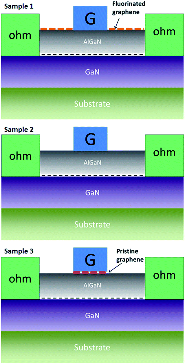 | ||
| Fig. 1 Schematic cross-sectional view of Sample 1, 2 and 3. | ||
Results and discussion
The passivation of graphene to the AlGaN surface
For Sample 1, the graphene layer covered the AlGaN surface and was fluorinated to be insulating. Raman spectroscopy was employed to analyze the change in graphene induced by fluorination. As shown in Fig. 2, there are two sharp Raman peaks (G peak at 1582 cm−1 and 2D peak at 2672 cm−1) in the pristine graphene just transferred to the surface of Sample 1, separately corresponding to the optical E2g phonons at the Brillouin zone centre and a second-order process involving two TO phonons near the K point.18 With regard to the intensity ratio of the 2D and G peak, the value ∼2.0 is consistent with the known features of monolayer graphene.19 After exposure to SF6 plasma for 180 s, the intensity and width of the G peak decreases, along with the increase of the D peak and disappearance of the 2D peak. The D peak is due to the breathing modes of the six-atom rings and requires a defect for its activation.18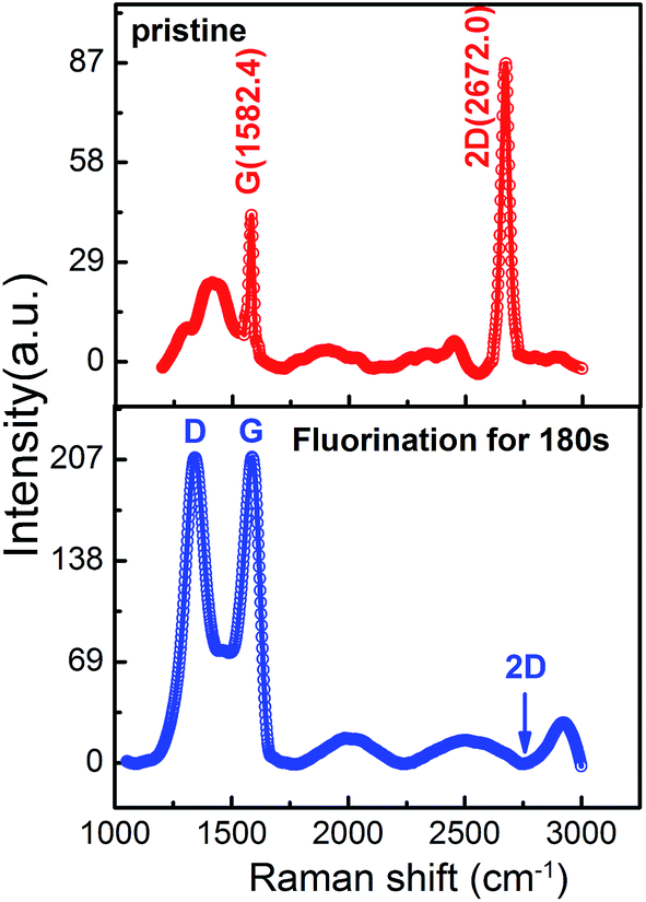 | ||
| Fig. 2 Raman spectra of the pristine and fluorinated graphene, respectively. | ||
The large intensity and width of the D peak indicates that graphene reacts with the plasma and fluorination induces fluorine defects to carbon bonds. Meanwhile, the defects perturbing the electronic states and decreasing its life time are responsible for the weakness of the 2D peak.20
To confirm the coverage of graphene on the diode surface, SEM and micro-Raman mapping analyses were done for Sample 1. The ripple is observed in SEM images (Fig. 3(a) and (b)), indicating that the fluorinated graphene completely covers the diode surface except for a small bare area near the metal edge coming from the graphene transfer process. The red dotted line region (14 μm × 14 μm) in the SEM image was scanned with Raman mapping. As shown in Fig. 3(c) and (d), D and G peaks exist and smoothly change with intensity from 100 to 200, which further illuminated the continuous and homogeneous coverage of fluorinated graphene on the device surface. The inset shows a single Raman spectrum of the graphene on Sample 1 after fluorination.
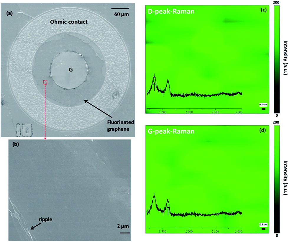 | ||
| Fig. 3 (a) Top-view SEM image of Sample 1. (b) SEM image of the region highlighted with a dotted red line (14 μm × 14 μm) in (a). (c) Raman mapping of D peak intensity in the region shown in (b). (d) Raman mapping of G peak intensity in the region shown in (b). Inset shows a single Raman spectrum of the graphene on Sample 1 after fluorination. | ||
The gate current was measured using an Agilent B1505A semiconductor parameter analyzer, where the gate bias was swept from −6 V to 5 V. As shown in Fig. 4(a), the gate current of Sample 1 with fluorinated graphene is lowered by about an order of magnitude in comparison with Sample 2 without graphene when the gate bias is below 2 V, and then two current curves trend to merge at a high gate bias. In addition, the turning point from low slope region to high slope region also shifts to a lower gate bias for Sample 1, namely Vt1 < Vt2.
 | ||
| Fig. 4 (a) Gate current density of Sample 1 (passivated with fluorinated graphene) and Sample 2 (unpassivated), (b) capacitance–voltage characteristic of Sample 1 around the turning point Vt1. | ||
Usually, the gate current (Jg) is composed of bulk leakage current (Jb) transporting through the metal–AlGaN/GaN junction and surface leakage current (Js). The difference of the gate current can only be due to surface leakage current since the bulk structure of Sample 1 is the same as that of Sample 2, except that the surface of AlGaN is passivated by fluorinated graphene. Fluorinated graphene can effectively suppress surface leakage current at low gate bias (Vg < Vt2) where surface defect leakage dominates and Schottky thermionic emission is relatively weak. Once the gate bias increases to a critical value at which electrons in the 2DEG channel can obtain enough kinetic energy to transport into AlGaN, which increases the electron density in AlGaN. The bulk current increases exponentially with a high slope factor and rises above the surface leakage current, and then the gate current curves merge together at high gate bias. Notice that the capacitance of Sample 1 begins to decrease gradually when the gate bias is beyond the turning point Vt1 as shown in Fig. 4(b). Sample 2 shows the same capacitance characterization but is not illustrated here. The reduction of the capacitance arises from the enhanced conductance of the AlGaN layer, which means electrons from 2DEG begin to transport into the AlGaN layer and thermally emit to form gate current. The capacitance change with the gate bias supports the speculation that the gate current increase rapidly after turning point.
In order to clearly interpret the gate current characteristics, diode models are utilized to describe the behavior happening at the metal/AlGaN Schottky barrier (diode 1), the interface between AlGaN and GaN (diode 2), and the AlGaN surface (diode 3), respectively. Diode 1 and diode 2 in series picture the bulk leakage current, and diode 3 presents the surface leakage current (Fig. 5). As shown in Fig. 5, the gate current density curve for Sample 1 with fluorinated graphene can be fitted with the thermionic emission current of diode 1, the Schottky barrier height of diode 1 is extracted to be 0.48 eV, which is lower than the difference between the metal work function and the semiconductor electron affinity, since the Schottky barrier formation also depends on the surface states of the semiconductor, which can cause Fermi level pinning.21 Before turning point Vt1, the electrons in 2DEG do not have enough kinetic energy to jump into AlGaN, and the electrons experiencing thermionic emission come from the generation–recombination process in the AlGaN layer. The electron population is small and the emission current increases with a low slope factor. Once the gate bias is beyond the turning point Vt1, electrons in 2DEG can obtain enough kinetic energy from the external electrical field to overcome the conduction band offset between AlGaN and GaN and inject into the AlGaN layer, when diode 2 turns on, and thermionic emission current increases rapidly. The process of the 2DEG injecting into AlGaN also can be confirmed by the capacitance’s decrease around the turning point as shown in Fig. 4(b). For Sample 2, the AlGaN surface, where uncovered by gate metal, is exposed to air, the surface leakage current modelled as the thermionic emission current of diode 3 is much larger than that of the bulk leakage current before the turning point Vt2, and dominates the gate current. The extracted Schottky barrier height is 0.26 eV for Sample 2, which further indicates the degradation of the Schottky barrier height by the AlGaN surface defects. Beyond Vt2, the bulk current shows a leading role, and the gate current density curves for two samples begin to merge. Finally the gate current density tends to saturate due to the electrode contact resistance. The ideality factors (IFs) for diodes were extracted according to Shockley’s theory. The calculated IF of diode 1, 2, 3 are 10, 5.5, 21, respectively. The electrons have to get across the Schottky barrier and adverse polarization electric field in AlGaN or trap-rich interface to form the gate current. During this process, the series resistance and recombination would induce a slow increase of gate current with gate bias. Consequently, the IFs are large, which are similar to those reported in ref. 21 and 22.
From the analysis of gate current for Sample 1 and Sample 2, it is concluded that fluorinated graphene can effectively suppress the surface leakage current. The mechanism may include two aspects: one is the neutralization effect of electrons in graphene on the positive charges existing at the AlGaN surface for there are a large amount of donor-like traps at the AlGaN surface, which usually are positively charged; another is the separation effect of the graphene membrane on the AlGaN surface and oxygen in air, which prevents the formation of Ga–O bonds and the formation of SDS. The leakage path along the surface is cut off and the barrier height between gate metal and AlGaN becomes high, and leads to the reduction of surface leakage current.
 | ||
| Fig. 5 The forward gate current density of Sample 1 and Sample 2 fitted by thermionic emission mechanism. The extracted Schottky barrier height for Sample 1 and Sample 2 before the turning point is 0.48 eV and 0.26 eV, respectively. Two diodes in-series (diode 1 and diode 2) depict the bulk leakage current and diode 3 models the surface leakage current. | ||
The passivation of graphene on the interface of gate metal and AlGaN
For Sample 1, fluorinated graphene covers the AlGaN surface but no graphene is under the gate metal. Fluorinated graphene can effectively passivate the AlGaN surface and suppress the surface leakage current. For Sample 3, the pristine monolayer graphene is just inserted at the interface of the gate metal and AlGaN to investigate the passivation effect. As a control, the structure of Sample 2 is the same as that of Sample 3 except that there is no graphene under the metal gate. The gate current and capacitance of Sample 3 are in comparison with Sample 2. As shown in Fig. 6, for Sample 3, the gate current density also can be reduced at reverse and forward gate bias, the capacitance decreases in the whole gate bias region, the flat band voltage shifts positively by about 0.45 V. In addition, the turning point Vt3 of Sample 3 is extremely close to Vt2, and is the crossing point of surface leakage current and bulk leakage. The difference between the gate current density and the capacitance should arise from the change of Schottky barrier height, surface donor-trap states, and dipole layers induced by the insertion of monolayer graphene into the interface of gate metal and AlGaN.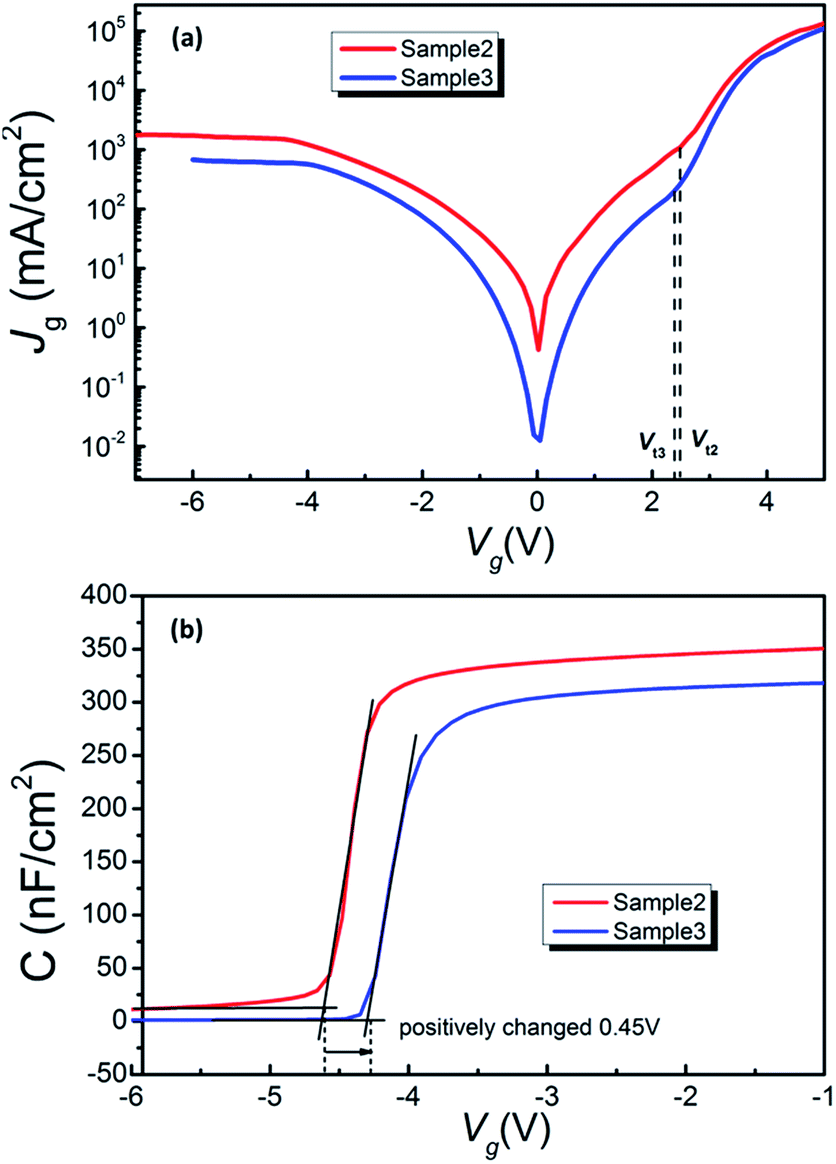 | ||
| Fig. 6 (a) Gate current density of Sample 2 (without graphene) and Sample 3 (with graphene under gate metal), (b) capacitance–voltage characteristic of Sample 2 and Sample 3. | ||
When graphene comes into contact with the metal and semiconductor, the electrons in graphene will transfer to the metal and surface donor-traps on AlGaN to realize the unity of Fermi level. Dipole layers form at the upper and lower surfaces of graphene, graphene becomes p-doping and its electronic states broaden, as shown in the energy band diagram of Fig. 7. Dipole layers behave like thin dielectric films, which reduces the total capacitance and influences the electron transmission probability to gate metal. In addition, graphene transfers electrons to the surface donor-like traps of AlGaN through the lower dipole layer, this process makes some of the surface donor-like traps electrically neutral, furthermore leading to the depletion of 2DEG at a higher gate bias, which is attributed to the positive shift of the flat band voltage. The extracted Schottky barrier height before the turning point is 0.38 eV, between 0.26 eV and 0.48 eV. It indicates that surface donor-like traps under gate metal also affect the surface leakage current, lowering the equivalent Schottky barrier height of surface leakage current. The graphene passivation layer, when it is on the AlGaN surface will improve the equivalent Schottky barrier height of surface leakage current more effectively; when it is under the gate metal it will reduce bulk current more efficiently.
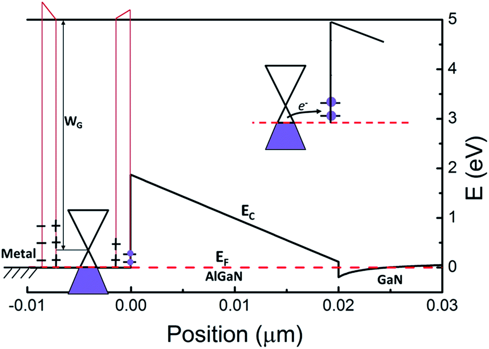 | ||
| Fig. 7 Conduction band diagram for the metal/graphene/AlGaN/GaN heterostructure at zero gate bias. The band diagram before graphene insertion was simulated by TCAD. The state after graphene insertion into the interface between the metal and AlGaN is shown in the schematic diagram. The inset shows the process of electrons transferring from graphene to donor-like traps on the AlGaN surface. | ||
Conclusions
The fluorinated insulating monolayer of graphene on the surface of the Schottky diode can effectively suppress the surface leakage current, leading to the reduction of the total gate current by one order of magnitude at reverse and low forward bias. Moreover, the pristine monolayer graphene under the gate metal can also reduce the gate current and shift the flat band voltage positively by 0.45 V. Surface donor-like traps of AlGaN provide a surface leakage path and also attract electrons into the 2DEG channel. Graphene can transfer electrons to neutralize part of the surface donor-like traps on the AlGaN surface and form a thin dipole layer. The reduction of surface donor-like traps can effectively suppress surface leakage current. The formation of a dipole layer helps to reduce bulk leakage current, and make 2DEG deplete at higher gate bias. The passivation effect brought out by graphene is attractive for the design of AlGaN/GaN HEMTs, which can increase the gate bias swing, threshold voltage, and suppress current collapse.Acknowledgements
This work was supported by the National Natural Science Foundation of China (grant no. 11175229).References
- L. Tsetseris and S. T. Pantelides, Carbon, 2014, 67, 58 CrossRef CAS PubMed.
- J. Scott Bunch, S. S. Verbridge, J. S. Alden, A. M. van der Zande, J. M. Parpia, H. G. Craighead and P. L. McEuen, Nano Lett., 2008, 8(8), 2458 CrossRef PubMed.
- H. Li, Z. Song, X. Zhang, Y. Huang, S. Li, Y. Mao, H. J. Ploehn, Y. Bao and M. Yu, Science, 2013, 342(6154), 95 CrossRef CAS PubMed.
- V. Berry, Carbon, 2013, 62, 1 CrossRef CAS PubMed.
- K. Sint, B. Wang and P. Kral, J. Am. Chem. Soc., 2008, 130(49), 16448 CrossRef CAS PubMed.
- S. C. O’Hern, C. A. Stewart, M. S. H. Boutilier, J.-C. Idrobo, S. Bhaviripudi, S. K. Das, J. Kong, T. Laoui, M. Atieh and R. Karnik, ACS Nano, 2012, 6(11), 10130 CrossRef PubMed.
- S. Hu, M. Lozada-Hidalgo, F. C. Wang, A. Mishchenko, F. Schedin, R. R. Nair, E. W. Hill, D. W. Boukhvalov, M. I. Katsnelson, R. A. Dryfe, I. V. Grigorieva, H. A. Wu and A. K. Geim, Nature, 2014, 516(7530), 227 CrossRef CAS PubMed.
- X. Zheng, M. Zhang, X. Shi, G. Wang, L. Zheng, Y. Yu, A. Huang, P. K. Chu, H. Gao, W. Ren, Z. Di and X. Wang, Adv. Funct. Mater., 2015, 25(12), 1805 CrossRef CAS PubMed.
- H. Nie, Q. Diduck, B. Alvarez, A. P. Edwards, B. M. Kayes, M. Zhang, G. Ye, T. Prunty, D. Bour and I. C. Kizilyalli, IEEE Electron Device Lett., 2014, 35(9), 939 CrossRef CAS.
- D. W. Seo, H. G. Choi, J. Twynam, Ki M. Kim, J. S. Yim, S.-W. Moon, S. Jung, J. Lee and S. D. Roh, IEEE Electron Device Lett., 2014, 35(4), 446 CrossRef CAS.
- C. Y. Tsai, T. L. Wu and A. Chin, IEEE Electron Device Lett., 2014, 33(1), 35 CrossRef.
- M. Wang and K. J. Chen, IEEE Trans. Electron Devices, 2011, 58(2), 460 CrossRef CAS.
- B. M. Green, K. K. Chu, E. M. Chumbes, J. A. Smart, J. R. Shealy and L. F. Eastman, IEEE Electron Device Lett., 2000, 21(6), 268 CrossRef CAS.
- S. Liu, S. Yang, Z. Tang, Q. Jiang, C. Liu, M. Wang, B. Shen and K. J. Chen, Appl. Phys. Lett., 2015, 106(5), 051605 CrossRef PubMed.
- Z. H. Liu, G. I. Ng, H. Zhou, S. Arulkumaran and Y. K. T. Maung, Appl. Phys. Lett., 2011, 98(11), 113506 CrossRef PubMed.
- M. Capriotti, A. Alexewicz, C. Fleury, M. Gavagnin, O. Bethge, D. Visalli, J. Derluyn, H. D. Wanzenböck, E. Bertagnolli, D. Pogany and G. Strasser, Appl. Phys. Lett., 2014, 104(11), 113502 CrossRef PubMed.
- Y. Wang, Y. Zheng, X. Xu, E. Dubuisson, Q. Bao, J. Lu and K. P. Loh, ACS Nano, 2011, 5(12), 9927 CrossRef CAS PubMed.
- A. C. Ferrari and D. M. Basko, Nat. Nanotechnol., 2013, 8(4), 235 CrossRef CAS PubMed.
- H. W. Qiu, S. C. Xu, P. X. Chen, S. S. Gao, Z. Li, C. Zhang, S. Z. Jiang, M. Liu, H. S. Li and D. J. Feng, Appl. Surf. Sci., 2015, 332, 614 CrossRef CAS PubMed.
- K. Tahara, T. Iwasaki, A. Matsutani and M. Hatano, Appl. Phys. Lett., 2012, 101(16), 163105 CrossRef PubMed.
- G. Fisichella, G. Greco, F. Roccaforte and F. Giannazzo, Nanoscale, 2014, 6(15), 8671 RSC.
- Y. Lv, Z. Lin, T. D. Corrigan, J. Zhao, Z. Cao, L. Meng, C. Luan, Z. Wang and H. Chen, J. Appl. Phys., 2011, 109(7), 074512 CrossRef PubMed.
| This journal is © The Royal Society of Chemistry 2015 |