
Asymmetric gold nanodimer arrays: electrostatic self-assembly and SERS activity†
Yuanhui
Zheng‡
*ab,
Lorenzo
Rosa
c,
Thibaut
Thai
bd,
Soon Hock
Ng
bd,
Daniel E.
Gómez
a,
Hiroyuki
Ohshima
e and
Udo
Bach
*abd
aMaterials Science and Engineering, Commonwealth Scientific and Industrial Research Organization, Clayton South, Victoria 3169, Australia
bThe Melbourne Centre for Nanofabrication, 151 Wellington Road, Clayton, Victoria 3168, Australia
cSwinburne University of Technology, Centre for Micro-Photonics (H34), P.O. Box 218, Hawthorn, Victoria 3122, Australia
dDepartment of Materials Engineering, Monash University, Wellington Road, Clayton, Victoria 3800, Australia. E-mail: Udo.Bach@monash.edu
eFaculty of Pharmaceutical Sciences, Tokyo University of Science, 2641 Yamazaki, Noda, Chiba 278-8510, Japan
First published on 22nd October 2014
Abstract
A simple, scalable, low-cost and high-throughput nanofabrication method is developed to produce discrete gold nanoparticle (AuNP) dimer arrays. This method involves a two-step electrostatic self-assembly: (1) electrostatic immobilization of negatively charged AuNPs onto a positively charged surface and (2) electrostatic adsorption of a positively charged AuNP onto each pre-assembled AuNP. The latter requires a careful control of the electrostatic energy barrier originating from the interactions between the charged AuNPs and surfaces. This can readily be achieved by tuning the ionic strength of the self-assembly media. We calculate the interaction energies for immobilizing a single positively charged AuNP onto each pre-assembled NP at different ionic strengths and present successful experimental results on the synthesis of high-yield symmetric and asymmetric AuNP dimers (dimer yield: ∼85%). A theoretical and experimental investigation of their optical properties is conducted to correlate the spectral properties of these dimers with their structure. We also study the SERS activity of the as-synthesized AuNP dimers using benzenethiol as a model analyte. It is found that, with the increase of the size dissimilarity between the two NPs in the dimers, the Raman intensities of the analyte increase gradually. This trend is completely different from those of both single AuNPs and AuNP aggregates with identical particle size.
Introduction
A unique feature of metal nanostructures is their ability to support localized surface plasmon resonances, which are light-driven coherent oscillations of free electrons in metallic nanostructures. When excited, surface plasmons can induce a large electromagnetic (EM) field enhancement in the close vicinity of the metal surface.1,2 The field enhancement is particularly strong at small interparticle gaps due to localized surface-plasmon coupling between two adjacent nanoparticles (NPs).1,2 The strength of the EM field at interparticle junctions is of importance for a broad variety of applications, such as molecular sensing,3–5 nonlinear optics,6,7 optical manipulation,8 and data storage.9 To date, complex metal NP assemblies, such as dimers, trimers, core-satellite nanostructures, one-dimensional (1D) NP chains, 2D NP films and 3D NP crystals, have been developed.10 Among all of these architectures, dimers are of special interest for two reasons. Firstly, the simplicity of this system makes it an ideal model for theoretical simulation studies. Secondly, an EM field enhancement in the gap region of metallic dimers as high as ∼104 has been predicted,2,11 enabling surface enhanced Raman scattering (SERS) signals to be detected with single-molecule sensitivity.12Over the past decades, considerable effort has been devoted to the development of nanofabrication methods that allow a reproducible synthesis of discrete plasmonic nanostructures such as metal NP dimers. Top-down lithographic techniques such as electron beam lithography (EBL)3,13 and angle-resolved nanosphere lithography14 have been used to generate arrays of periodic metal NP dimers. However, these methods yield polycrystalline nanostructures. This generally leads to increased damping of the plasmonic oscillation compared to single crystalline metal NPs with defect-free crystal facets synthesized through chemical routes.15 The latter can be used as building blocks for the assembly of complex nanostructures. They can be synthesized with excellent monodispersity in size and shape down to the nanometer range. More importantly, self-assembly allows the control of the spacing between metal NP building blocks with sub-nanometer resolution through choice of the appropriate linker molecules.16 Self-assembled metal nanostructures show particularly high EM field enhancements for narrow gaps in the sub-5-nanometer range, which are difficult to realize with lithographic techniques.
Kinetic aggregation is one of the simplest self-assembly methods in which the assembly is triggered by a change in the environmental medium, such as salt concentration17–21 and solvent composition.22–24 For example, Chen et al. reported the use of salt to induce NP aggregation in colloidal solutions and achieved an initial dimer yield of roughly 24%.20 The dimers were subsequently enriched to 95% through gradient centrifugation.20 In comparison with random aggregation, controlled self-assembly strategies are more attractive for fabricating metal NP dimers as they allow us to specifically construct asymmetric dimers, composed of two distinguishable building blocks. These methods rely on the anisotropic functionalization of metal NPs with “binding patches” derived from biological12,25–29 or organic molecules.16,30,31 The NPs are considered as “artificial molecules” that can undergo specific reactions to yield metal NP dimers in solution. Apart from self-assembly in solution, template-directed assembly of dimers onto a recessed patterned surface driven by the capillary force has also been demonstrated.32–34 Rivera et al. reported the use of convective-capillary forces to trap metal NPs in the recessed regions of a patterned substrate.34 They found that, even under optimal assembly conditions, only 59% of the resulting assemblies are dimers, the remaining assemblies correspond to monomers (2%) and multimers (39%). Despite these significant advances in NP dimer fabrication, self-assembly of asymmetric dimers with high yield still remains challenging.
In this work, we develop a low-cost, non-lithographic and scalable method to produce a high surface coverage of discrete plasmonic dimers. This method involves a two-step electrostatic self-assembly: (1) electrostatic immobilization of negatively charged NPs onto a positively charged surface and (2) electrostatic adsorption of one positively charged NP onto each pre-assembled NP. This two-step self-assembly provides the opportunity to synthesize symmetric and asymmetric dimers, simply by choosing NPs that vary in composition, shape or size for steps (1) and (2). The latter requires the careful tailoring of the prevailing electrostatic energy barriers with respect to thermally induced Brownian motion (i.e. 1.5 kBT, kB: Boltzmann constant; T: absolute temperature) of the approaching particle. We therefore calculated the interaction energy for immobilizing a single NP onto each predefined adsorption site and presented successful experimental results on the fabrication of discrete AuNP dimers. Symmetric and asymmetric AuNP dimers with a yield of ∼85% were successfully fabricated. A theoretical and experimental investigation of their optical properties was conducted to correlate the spectral properties of these dimers with their structure. We also studied the SERS activity of the as-synthesized AuNP dimers using benzenethiol as a model analyte and found that the particle size dissimilarity of the dimers plays an important role in increasing their SERS performance.
Experimental
Synthesis of DNA–AuNP conjugates
Commercially available spherical AuNPs (average diameter: 30 nm, Ted Pella) were functionalized with monothiolated DNA according to a method described previously.5,35,36 In a typical procedure, 1 mL of citrate-stabilized AuNP solution with an optical density of 1.0 was concentrated to 100 μL by centrifugation (Eppendorf 5415R centrifuge; 4000 rpm, 45 min). 5 μL of 2.0% polyoxyethylene (20) sorbitan monolaurate (Tween 20, Sigma-Aldrich), 30 μL of 0.1 M phosphate buffer (pH = 7.0), 50 μL of 2.0 M NaCl, 20 μL of 100 μM monothiol DNA solution (sequence: 5′-[HS]-T15-TTA TGA CCC TGA TTA-3′, Fidelity Systems Inc.) and 5 μL of 0.1 M bis(p-sulfonateo-phenyl)phenylphosphine dihydrate dipotassium salt (BSPP, Sigma-Aldrich) were added to the AuNP solution. The mixture was incubated at room temperature overnight. The DNA–AuNPs were washed 5 times with fresh Millipore™ water. After the final washing step, the DNA–AuNPs were redispersed in 1 mL of fresh Millipore™ water.Synthesis of TMAC–AuNP conjugates
Commercially available spherical AuNPs (Ted Pella) with different sizes (30 nm, 40 nm, 50 nm and 60 nm) were functionalized with N,N,N-trimethyl-(11-mercaptoundecyl)ammonium chloride (TMAC, ProChimia). In a typical procedure, 1 mL of citrate-stabilized AuNP solution with an optical density of 1.0 was washed with fresh Millipore™ water once and concentrated to 100 μL by centrifugation. A given volume of 12 mM TMAC was added into the AuNP solution, followed by addition of 100 μL of 6 mM cetyltrimethylammonium bromide (CTAB, Sigma-Aldrich) solution. The molar ratio between TMAC and AuNPs was controlled to be 4.6 × 10⁴ for all samples (see Table 1 for details). The mixture was incubated for 12 hours at room temperature. The resulting TMAC–AuNPs were washed 5 times with air-equilibrated Millipore™ water. Note that the TMAC–AuNPs start to partially precipitate at the second wash step if fresh Millipore™ water is used for washing. After the final washing step, the TMAC–AuNPs were redispersed in 400 μL of air-equilibrated Millipore™ water (optical density: 2.5).| AuNPs | 12 mM TMAC/μL | 6 mM CTAB/μL | Incubation time/h |
|---|---|---|---|
| 30 nm | 12.6 | 100 | 12 |
| 40 nm | 5.7 | 100 | 12 |
| 50 nm | 2.4 | 100 | 12 |
| 60 nm | 1.5 | 100 | 12 |
APTES modification of silica-coated silicon substrates
Silica-coated (thickness: 100 nm) silicon and glass (4 × 6 mm2) substrates were modified with 3-aminopropyltriethoxysilane (APTES) by immersion into a mixture of APTES, water, and ethanol at a volume ratio of 2![[thin space (1/6-em)]](https://www.rsc.org/images/entities/char_2009.gif) :3:95 for 1 h. It was then washed with ethanol three times, dried under a stream of nitrogen, and baked at 110 °C for 10 min.
:3:95 for 1 h. It was then washed with ethanol three times, dried under a stream of nitrogen, and baked at 110 °C for 10 min.
Self-assembly of AuNP dimers
In a typical procedure, an APTES modified glass or silica-coated silicon substrate was placed in a centrifuge tube containing 200 μL of 0.033 nM DNA–AuNP solution and then incubated at 65 °C for 2 hours. The substrate was washed five times with fresh Millipore™ water and then dried under a stream of nitrogen. The substrate was then immersed in 200 μL of the TMAC–AuNP solution (optical density: 2.5) containing a given concentration of NaCl (see Table 2 for details). The mixture was incubated at 25 °C for 3 hours. Finally, the substrate was washed three times with fresh Millipore™ water and then dried naturally in air.| Dimers | [TMAC–AuNPs] | [NaCl]/μM | Temperature/°C | Incubation time/h | |
|---|---|---|---|---|---|
| Optical density | Volume per μL | ||||
| 30–30 nm | 2.5 | 200 | 12.5 | 25 | 3 |
| 30–40 nm | 2.5 | 200 | 15 | 25 | 3 |
| 30–50 nm | 2.5 | 200 | 20 | 25 | 3 |
| 30–60 nm | 2.5 | 200 | 25 | 25 | 3 |
Fabrication of SERS substrates
In order to avoid any Raman signal interference from the surface-confined molecules on the self-assembled AuNP dimers, the surface-confined molecules were replaced by dithiothreitol (DTT) via a classical thiol exchange reaction.48 The surface-confined DTT can be completely removed through subsequent UV-ozone treatment. Prior to DTT treatment, the substrates were exposed to 200 μL of a solution containing 2 mM sulfosuccinimidyl-4-(N-maleimidomethyl)cyclohexane-1-carboxylate (sulfo-SMCC) and 10 mM phosphate buffer (pH = 7.5) at 45 °C for 3 h. Following the sulfo-SMCC treatment, the substrates were then immersed into 200 μL of 0.5 M DTT solution overnight. Sulfo-SMCC is employed to link the dimers to the substrate and DTT-confined AuNP dimers. The sulfo-NHS ester of sulfo-SMCC reacts with amino groups on the substrate and its maleimide functionality reacts with DTT bound to the AuNPs. Following the DTT treatment, the substrates were exposed to UV-ozone at an oxygen flow of 0.5 L min−1 for 20 min to remove DTT. After the UV-ozone treatment, the substrates were immersed into 2 mL of 1 μM thiolbenzene ethanolic solution overnight, washed with ethanol 3 times and then dried in a desiccator purged with nitrogen.Characterization
Scanning electron microscopy (SEM) and atomic force microscopy (AFM) images of the self-assembled AuNP dimers were taken with a JEOL 7001F field emission SEM and an Agilent Technologies 5500 AFM, respectively. Since transparent substrates are required for UV-vis spectroscopy, glass wafers were used as supporting substrates for the AuNP dimers. The absorption spectra were recorded using a Cary 60 UV-vis spectrometer. Raman spectra of the AuNP dimers immobilized on silica-coated silicon substrates (silica thickness: 110 nm) were recorded using a Renishaw RM 2000 Confocal micro-Raman System equipped with a near-IR diode laser at a wavelength of 782 nm (laser power: 1.15 mW, laser spotsize: 1 μm2). All of the Raman spectra were collected by fine-focusing a 50× microscope objective and the data acquisition time was 10 s.Theoretical modeling
Three dimensional finite-difference time-domain (3D-FDTD) simulations were performed on a single dimer, enclosed in a domain with a size of 0.2 × 0.2 × 0.4 μm3. The square mesh size was 0.2 nm.Results and discussion
To produce a high surface coverage of discrete AuNP dimers we have adopted a hierarchical electrostatic self-assembly strategy, as illustrated in Scheme 1. In a typical procedure, positive surface charges were conferred onto a silica-coated (thickness: 110 nm) silicon substrate by immersing the substrate into an ethanolic solution containing APTES (Scheme 1a). The resulting amino-terminated surface is positively charged at neutral and lower pH.37 Commercially available spherical AuNPs (diameter: 30 nm, Ted Pella) functionalized with monothiolated DNA8,35,36 (DNA–AuNPs) were used as building blocks to generate a high surface coverage of adsorption sites on the APTES-modified substrate. Exposing the substrate to the negatively charged DNA–AuNPs results in particle adsorption mediated by electrostatic interactions (Scheme 1b). These surface-confined particles serve as single adsorption sites for subsequent NP self-assembly. Following the DNA–AuNP immobilization (step 1), the substrate is exposed to a solution containing TMAC–AuNPs. These positively charged NPs were synthesized by functionalization of citrate-stabilized AuNPs (Ted Pella) with TMAC. This process involves a change of the particle surface charge from negative to positive. Removal of free citrate ions from the colloidal AuNP solution by washing with fresh Millipore™ water is critical for the synthesis of stable TMAC–AuNPs. Careful control over the ionic strength of the TMAC–AuNP solution at assembly step 2 results in the adsorption of a single TMAC–AuNP onto each DNA–AuNP, driven by the electrostatic and van der Waals attractions between the NPs, predominantly leading to the formation of dimers (Scheme 1c). Symmetric and asymmetric dimers are obtained by varying the size of the TMAC–AuNPs. | ||
| Scheme 1 A schematic representation of the hierarchical electrostatic self-assembly procedure. (a) APTES functionalization of a silica-coated silicon substrate; (b) DNA–AuNP (30 nm diameter) arrays fabricated by an electrostatic self-assembly technique, which act as adsorption sites for (c) subsequent electrostatic assembly of a single TMAC–AuNP with particle size varying from 30 nm to 60 nm, forming symmetric (30–30 nm) and asymmetric (30–40 nm, 30–50 nm and 30–60 nm) AuNP dimers. | ||
The successful self-assembly of dimers with high surface coverage depends critically on two capabilities. Firstly the ability to control the distance between self-assembled NPs in assembly step 1. This is vital to achieve high levels of surface coverage while maintaining a minimum distance between neighboring dimers to avoid coupling. The electrostatic adsorption process used in this approach is particularly advantageous in this respect. Here the repulsive electrostatic interparticle forces and their partial screening through the surrounding ionic medium predetermine the separation between neighboring particles during the assembly. These forces ultimately depend on parameters such as the NP concentration, the NP surface charge, the ionic strength of the medium and its temperature. All of these can be experimentally controlled. Importantly, we have recently shown that the nearest neighbor distance resulting from an electrostatic assembly process shows a narrow, non-stochastic distribution.5 The electrostatic self-assembly of 30 nm DNA–AuNPs in step 1 was conducted by immersing an APTES-modified substrate into a 65 °C DNA–AuNP solution with a particle concentration of 3.3 × 10⁻¹¹ M for 2 hours. A high surface coverage of discrete AuNPs with an average nearest-neighbor distance of approximately 160 nm was achieved (Fig. S2†).
The second critical step is to control the number of NPs that adsorb onto each anchoring particle previously deposited. This assembly process needs to be self-limiting, providing favorable conditions for the binding of a single positively charged particle while impeding the subsequent adsorption of additional particles onto already formed dimers. A simple electrostatic consideration shows that, as a TMAC–AuNP approaches the substrate from afar, the attractive electrostatic forces originating from the surface-confined DNA–AuNPs are screened by the repulsive electrostatic forces that stem from the positively charged substrate. As the TMAC–AuNPs draw closer to the DNA–AuNPs, the attractive force will at some point overcome the repulsive force emanating from the APTES modified substrate, resulting in an overall attractive force that actively drives the adsorption of the TMAC–AuNPs to the DNA–AuNPs. The repulsive forces that prevail during the initial phase of the approach give rise to an activation barrier for the TMAC–AuNP adsorption process. This energy barrier needs to be carefully tuned with respect to the thermal energy (1.5 kBT) of the approaching TMAC–AuNPs, to allow for the formation of dimers at high yields. At the same time, the barrier should be kept as high as possible to avoid binding of multiple TMAC–AuNPs onto a single DNA–AuNP. The latter process will result in the undesirable formation of trimers, tetramers and even large agglomerates – a process that can be observed when the ionic strength of the assembly media is increased excessively (Fig. S4†).
To understand this electrostatically driven assembly more clearly, we calculated the interaction energies between a TMAC–AuNP and a surface-confined DNA–AuNP based on the Derjaguin, Landau, Verwey and Overbeek (DLVO) theory.38 We plotted the calculated results in Fig. 1 (see ESI† for calculation details). When a 30 nm TMAC–AuNP approaches a DNA–AuNP at an angle perpendicular to the APTES modified substrate (Fig. 1a) under low ionic strength conditions (i.e. salt-free conditions), the TMAC–AuNP is repelled electrostatically by the background positive charges of the substrate (green curve), but is also attracted by the negative charges of the DNA–AuNP (red curve) and the van der Waals attraction forces (at shorter distances) originating from the DNA–AuNP and the substrate (orange curve). The total interaction energy (blue curve) between the positively charged NP and the substrate with negatively charged NPs is the sum of the contributions of the electrostatic interaction energies and the van der Waals energy. As shown in Fig. 1a, the total interaction energy curve shows a maximum energy barrier of ∼96 meV (i.e. ∼4 kBT) at a particle–substrate distance of ∼120 nm and a primary energy minimum (Emin) of −2.28 eV at a particle–particle distance of 1 nm. This constitutes a high-energy barrier compared to the average thermal energy of the TMAC–AuNPs of 1.5 kBT (∼39 meV),39 suggesting that dimer formation yields should be low. This is in agreement with the experimental observations (Fig. S3†).
 | ||
| Fig. 1 Calculated interaction energies. (a) An example of the interaction energies between a 30 nm TMAC–AuNP and a 30 nm DNA–AuNP on a silica-coated silicon substrate in air-equilibrated Millipore™ water (ionic strength ≈ 13.3 μM). Ee,r is the electrostatic repulsion energy between the TMAC–AuNP and APTES-modified substrate; Ee,a is the electrostatic attraction energy between the TMAC–AuNP and DNA–AuNP; EvdW is the van der Waals interaction energies between the TMAC–AuNP and DNA–AuNP as well as the APTES modified substrate; Emin is the primary energy minimum at an interparticle distance of 1 nm; and z is the particle–substrate distance; (b) an example of the total interaction energy between a 30 nm TMAC–AuNP and a surface-confined 30 nm DNA–AuNP on a silica-coated silicon substrate at different ionic strengths; (c) calculated energy barriers for the formation of AuNP dimers as a function of ionic strength (for panels a–c), the calculations were conducted assuming that the TMAC–AuNP is approaching at an angle perpendicular to the APTES modified substrate, see the inset of panel (a); and (d) calculated energy barriers for the formation of AuNP dimers as a function of approaching angle, θ. | ||
A simple way of controlling electrostatic interaction energies is by fine-tuning the ionic strength of the assembly medium. Fig. 1b shows the calculated energy barriers for single TMAC–AuNP adsorption as a function of the ionic strength of the adsorption medium. The figure reveals a drastic decrease of the activation barrier well below the thermal energy as the ionic strength of the medium is increased from 15 μM to 40 μM. The decrease of the energy barrier makes TMAC–AuNP adsorption more favorable. Experimentally we found that the yield of 30–60 nm dimers increases when the NaCl concentration is increased from 0 μM to 20 μM (Fig. S4†). For a NaCl concentration of 30 μM the dimer yield is slightly decreased. A further increase of the NaCl concentration to 1 mM results in the non-specific adsorption of TMAC–AuNPs on the substrate surface (Fig. S4†). Fig. 1c shows the calculated activation barrier heights as a function of the ionic strength of the assembly medium for TMAC–AuNPs with radii of 30, 40, 50 and 60 nm. The attractive and repulsive interaction energy terms both increase with increasing radii, resulting in an overall increase of the energy barrier (Fig. 1c). The energy barriers for the self-assembly of 30–30, 30–40, 30–50 and 30–60 nm dimers under ionic strength conditions, which experimentally produced the highest dimer yields, are found to be ∼43 meV (slightly higher than the thermal energy, ∼39 meV of the TMAC–AuNPs). Further calculations also reveal that this activation barrier is dependent on the angle at which the TMAC–AuNP is approaching the surface (Fig. 1d). It increases drastically with increasing approach angle, forming a repulsive potential well. When the TMAC–AuNP is being attracted to the DNA–AuNP, the gradient of the repulsion potential in a direction parallel to the substrate produces a lateral force that pushes it toward the lowest energy site, guiding the particle adsorption to the top center of the DNA–AuNP. This phenomenon has been previously observed when electrostatically placing single NPs onto EBL defined nanopatterns35,38,40 and is described as the electrostatic funnel guiding effect.38,40 The formation of trimers by adsorption of a TMAC–AuNP onto a pre-formed dimer is less favorable due to the additional repulsive forces between the pre-assembled and approaching TMAC–AuNP (Fig. S5†). As discussed above, in solution the energetically most favorable position of the TMAC–AuNP in a dimer is vertically above the DNA–AuNP, along the surface normal of the substrate. In this case, the attractive force between the approaching TMAC–AuNP and the surface confined DNA–AuNP is screened by the repulsive force between the two TMAC–AuNPs. Calculations also show that even in the unlikely case where the first TMAC–AuNP is located beside the DNA–AuNP, the energy barrier for the approach of a second TMAC–AuNP is still sufficiently high to suppress trimer formation (Fig. S5†).
Fig. 2 shows SEM and AFM analyses of the resulting AuNP dimers. The typical SEM and AFM micrographs clearly show the successful formation of symmetric and asymmetric AuNP dimers on silica-coated silicon substrates. Interestingly, most of the AuNP dimers shown in the SEM and AFM images appear to adapt a lateral configuration (i.e. lateral dimers) where the TMAC–AuNP is located in the close vicinity of the silica-coated silicon substrate. According to the electrostatic funneling theory,38,40 the lowest energy state is the one where the TMAC–AuNP sits vertically on the top of the pre-assembled DNA–AuNPs (i.e. vertical dimers). The latter configuration is also presented and evidenced in the AFM images and the cross-sectional profiles. With the increase of TMAC–AuNP size, the yield of vertical dimers decreased from ∼25% to 1%. This could be explained by a configuration change during the drying step driven by capillary forces. To confirm the conformational change, we analyzed the dimer samples before and after drying using UV-vis spectroscopy (see Fig. S6†). Prior to drying, a major absorption peak at 525 nm with a shoulder located at 610 nm is observed. The major peak is attributed to the excitation of the surface plasmon mode that is perpendicular to the long axis of the dimers (i.e. transverse plasmon),41 while the shoulder might be due to the excitation of the surface plasmon mode that is parallel to the long axis of the dimers (i.e. longitudinal plasmon). This indicates that the majority of the resulting dimers before drying are vertical dimers. After drying, the intensity of the peak at longer wavelength increases drastically. The evolution of absorption peaks indicates the change of dimer conformation from vertical to horizontal during the drying process. Statistical analysis of the assemblies based on low-magnification SEM (Fig. S7†) and AFM micrographs reveals that approximately 85% of the assemblies are dimers, the rest correspond to individual AuNPs (i.e. monomers: ∼10%), trimers (∼5%) and uncontrolled aggregates (<0.5%).
 | ||
| Fig. 2 Micrographs and statistical analysis of metal nanoparticle dimers. (a–d) SEM and (e–h) AFM micrographs of AuNP dimers with different particle sizes on silica-coated silicon substrates fabricated through the electrostatic self-assembly procedure illustrated in Scheme 1; (i–l) cross-sectional profiles of the AuNP dimers 1 (red curve) an 2 (blue curve) highlighted in the corresponding AFM micrographs shown in the second column; and (m–p) SEM-image (green bars) and AFM-image (blue bars) based statistical analyses of the configuration distribution of the assemblies. Rows from top to bottom show 30–30 nm (symmetric) dimers, 30–40 nm dimers, 30–50 nm dimers and 30–60 nm dimers (second row to fourth row: asymmetric dimers). | ||
The optical properties of the as-fabricated AuNP dimer arrays on glass substrates (dry sample) were recorded using UV-vis absorption spectroscopy (Fig. 3a, solid curves). The surface immobilized DNA–AuNP array shows similar optical properties to that of colloidal aqueous DNA–AuNP solutions, exhibiting a single dipolar-plasmon resonance peak at 525 nm (maroon solid curve). After exposure to a TMAC–AuNP solution, the maximum absorption of all samples significantly increases. With increasing TMAC–AuNP particle size the plasmon absorption peak of the as-synthesized dimers splits into two distinct peaks. To describe semi-quantitatively the surface plasmon resonances of the dimers, we modeled their absorption spectra using the electrostatic Eigen mode method (see ESI† for modeling details).42,43 The surface plasmon resonances of the sphere dimers can be broadly categorized into (1) axial modes: those in which the net dipole moment of the plasmon resonance is aligned with the axis joining the nanosphere centers and (2) transverse modes: those in which the dipole modes are aligned perpendicular to these axial modes. In this way the optical absorption spectrum of NP dimers depends strongly on the polarization of the incident light beam with respect to the axis connecting both particles. Additionally, the wavelength positions of these resonances depend on the refractive index of the medium surrounding the particles and their separation distance. By carefully adjusting the interparticle distance in our modeling, we were able to reproduce the qualitative features of the measured absorption spectra (Fig. 3a, dashed lines). To further confirm the simulated results, we calculated the absorption cross-sections and the maximum electric field enhancement of the dimers using the 3D-FDTD method.44 The peak positions of simulated absorption cross-sections obtained by the 3D-FDTD method (Fig. S11†) are in good agreement with those shown in Fig. 3a. Fig. 3b shows the electric field enhancement as a function of wavelength in the range of 400–900 nm. A distinct peak of enhancement between 550 nm and 600 nm is observed for all dimers, which is ascribed to the dipolar modes of surface plasmons. Fig. 3c shows the simulated surface charge distribution across the cross-section of the 30–60 nm dimers at a wavelength of 580 nm. The circles with two different colors emphasize the transitions between positive (red) and negative (blue) charge, confirming the dipole nature of the fundamental mode. The spatial electric field distributions of the dimers at an excitation wavelength of 782 nm (Fig. 3d) show that the electric field and the volume of the hot spots increase with increasing size dissimilarity (details are summarized in Table 9 of ESI†).
 | ||
| Fig. 3 Optical properties and electromagnetic field enhancement of metal nanoparticle dimers. (a) Experimental (solid lines) and calculated absorption spectra (dashed lines) of the symmetric and asymmetric AuNP dimers (a gap of 1 nm is employed for modeling). The slight difference between the experimental and calculated spectra is due to the size and geometrical deviation of the nanoparticle building blocks. (b) Maximum electric field intensity enhancement at the middle of the gap of a dimer with longitudinal excitation. (c) Surface charge distribution of 30–60 nm dimers at a wavelength of 580 nm. The circles with two different colors emphasize the transitions between positive (red) and negative (blue) charge. (d) Spatial distribution of electromagnetic field enhancement of the metal nanoparticle dimers in the xz-plane at a wavelength of 782 nm. | ||
One application of the as-fabricated dimers is molecular sensing based on surface-enhanced Raman signals near the nanostructures. The plasmon coupling within a pair of metal NPs has previously been used to generate strongly confined and enhanced EM fields within the gap (i.e. hot spot) between the pair, making the Raman signals of analytes sitting within the gap highly active.12 It has been demonstrated that the SERS activity of a plasmonic nanostructure is critically dependent on the number and geometry of its hot spots. To evaluate the SERS performance of the symmetric and asymmetric dimers, benzenethiol was adopted as a model analyte. DNA is known to be a Raman-active molecule, in which the Raman bands largely arise from base and phosphate vibrations.46–48 Typical DNA Raman bands can be observed in three regions: (1) 600–800 cm−1: aromatic in-plane bending vibrations of the bases; (2) 800–1200 cm−1: stretching vibrations of the phosphate moiety; and (3) 1200–1700 cm−1: aromatic stretching vibrations of the bases.45–47 To avoid Raman signal interference from the surface-confined DNA strands, we displaced the surface-confined DNA strands, with DTT, which can be completely removed via UV-ozone treatment. Exposure of surface-immobilized layers of monothiolated, single-stranded DNA to DTT has previously been shown to lead to a complete replacement of DNA via a classical thiol exchange reaction.48 SEM analysis showed that the replacement of DNA with DTT can result in the rearrangement of the dimers on the substrate due to the decrease of electrostatic attractions between the AuNPs and the substrate, forming larger aggregates. To solve this problem, a bifunctional linker, sulfo-SMCC, was employed to link the dimers to the substrate. This was done by immersing the as-fabricated dimers into a 2 mM sulfo-SMCC solution for 3 hours, then into a 0.5 M DTT solution overnight. The sulfo-NHS ester of sulfo-SMCC reacts with amino groups on the substrate and its maleimide functionality reacts with DTT bound to the AuNPs. Following the DTT treatment, all substrates were exposed to UV-ozone to remove DTT and then immersed into a 1 μM solution of thiolbenzene in ethanol overnight prior to the SERS experiments. After the thiol exchange, UV-ozone treatment and analyte loading, no obvious aggregation of dimers is observed (Fig. S12†) and the absorption peak at shorter wavelength does not shift while the one at longer wavelength slightly redshifts (Fig. S13†). The redshift of the second peak is indicative of a reduction in interparticle gap.5,49 For each SERS measurement, a Raman probe laser with an excitation wavelength of 782 nm and spot size of 1 μm2 was focused onto the substrate surface. Fig. 4a compares the Raman spectra of benzenethiol adsorbed on the self-assembled AuNP dimers. Strong fingerprint peaks of benzenethiol50 at 999, 1022, 1073 and 1573 cm−1 were observed for all the samples. An excellent correlation between the peak positions and the relative intensities of benzenethiol was observed for all samples. For each sample, the 1075 cm−1 Raman peak height was measured at five different spots. The average signal height for each sample is plotted in Fig. 4b (grey bars). With the increase of the size dissimilarity between the two NPs in the dimers, the SERS intensities of the analyte increase gradually. To understand how the EM field enhancement and geometry impact the SERS process, we evaluated the size of the hot spot at the 782 nm wavelength excitation and integrated the theoretical SERS enhancement factor |EL/E0|2|ER/E0|2 (L: laser; R: Raman) over the hot-spot volume (see ESI† for details). The integrals of the SERS enhancement factor increase from 30–30 nm dimers to 30–60 dimers (Fig. 4b, red bars), which is in good agreement with the experimental results (Fig. 4b, grey bars). These data reveal that the increased SERS intensity with increasing particle size dissimilarity is due to the increase of both EM field enhancements in the hot spots and hot-spot volume. Surprisingly, the SERS activity trend observed here is significantly different from those for both single AuNPs51 and AuNP aggregates with identical particle size.52 It has been reported that, for both single AuNPs and AuNP aggregates with identical particle size, the SERS activities increase first and then decrease as the particle size increases. The highest SERS activity for AuNP aggregates was found at a particle size of about 46 nm when excited with a 785 nm laser.51
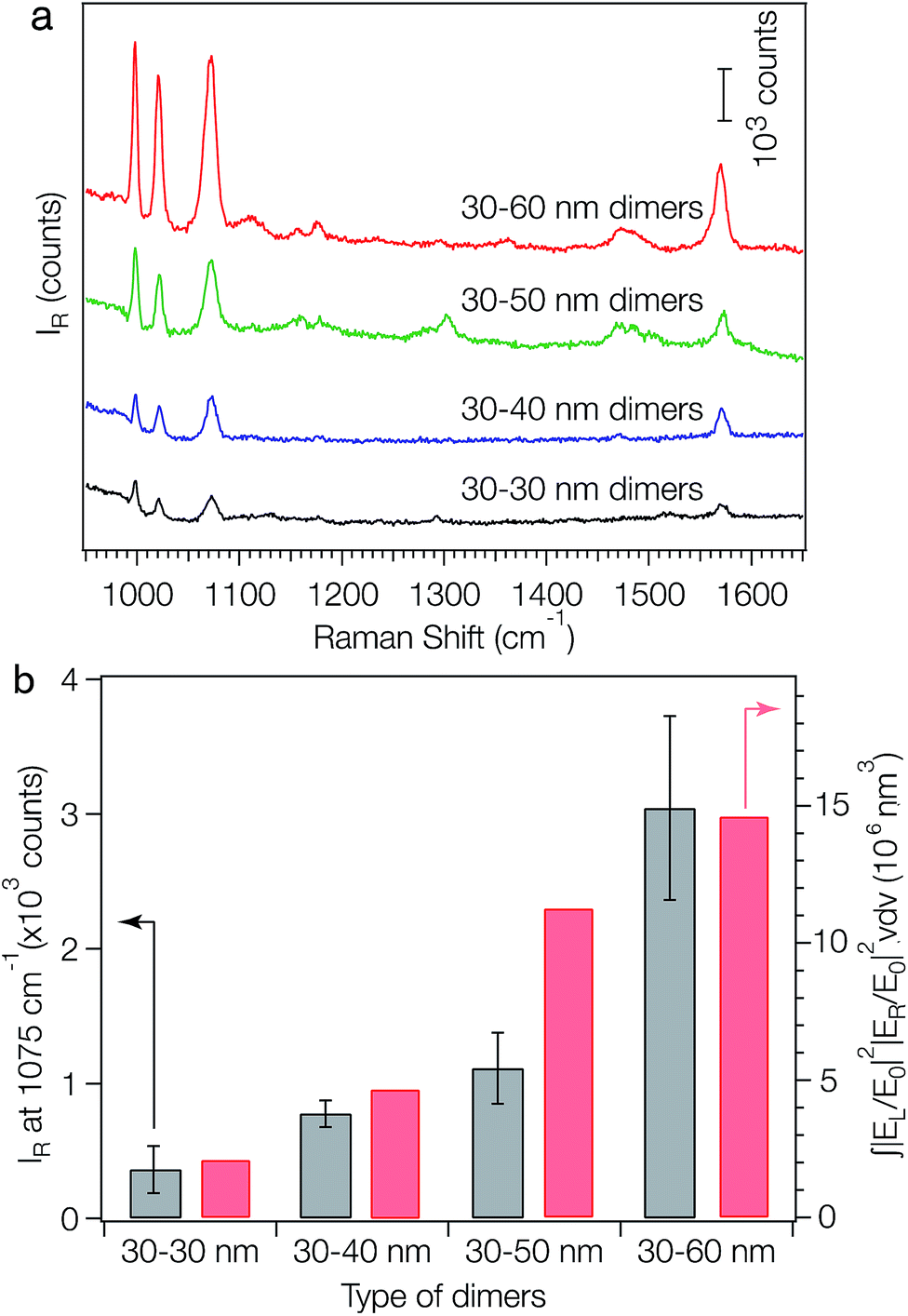 | ||
| Fig. 4 SERS activities of metal nanoparticle dimers. (a) SERS spectra of benzenethiol (loading concentration: 1 μM) adsorbed on the symmetric (30–30 nm) and asymmetric (30–40 nm, 30–50 nm and 30–60 nm) AuNP dimers. (b) Experimental Raman intensities at peak 1075 cm−1 of the dimers (grey bars) and the integral of the simulated SERS enhancement factors (red bars) over the hot spots shown in Fig. 3d, at an excitation wavelength of 782 nm. For all samples, λex = 782 nm, Pex = 1.15 mW, acquisition time = 10 s. | ||
Conclusions
In conclusion, we have developed a simple self-assembly method for the reproducible synthesis of symmetric and asymmetric AuNP dimers with high yield. This is based on a two-step electrostatic self-assembly method. Negatively charged metal NPs are immobilized onto a positively charged substrate with tunable interparticle spacing, followed by the precise placement of a single positively charged NP on each pre-adsorbed negatively charged NP. Controlling interparticle and particle–substrate interactions is critical for the morphological selectivity in the assemblies. Symmetric and asymmetric AuNP dimers with a high yield of ∼85% were successfully fabricated without the need for expensive direct-write nanolithography techniques such as EBL. The dimer yield achieved in this work is unmatched by any previous self-assembly techniques. Furthermore, this approach is compatible with other building blocks such as polymers, quantum dots, etc., and adaptable for the fabrication of more complex NP assemblies including trimers, tetramers and core-satellite nanostructures.We also investigated the optical properties of the symmetric and asymmetric dimers and compared them to the theoretical results. Two types of surface plasmon resonance modes (i.e., the transverse and longitudinal modes) with a distinct redshift of the longitudinal plasmon resonance were observed when the particle size dissimilarity increases. The SERS activities of the dimers also scale with the particle size dissimilarity of the dimers. These results are in good agreement with the theoretical modelings. Moreover, this work represents a simple proof-of-concept experiment for the fabrication of plasmonic homodimers. The self-assembly method developed here can also be easily extended to the fabrication of compositional heterodimers with potential applications in catalysis.
Acknowledgements
The authors acknowledge financial support from the Australian Research Council through an Australian Research Fellowship (UB), a UNSW Vice-chancellor Fellowship (YZ) an Australian Postdoctoral Fellowship (D.E.G) and a Discovery Project DP110101767 (D.E.G). Further financial support has been received from Commonwealth Scientific and Industrial Research Organization through an OCE Science Leader position (UB). This work was performed at the Melbourne Centre for Nanofabrication (MCN) in the Victorian Node of the Australian National Fabrication Facility (ANFF). Part of this work was performed on the swinSTAR supercomputer at Swinburne University of Technology.Notes and references
- C. F. A. Negre, E. M. Perassi, E. A Coronado and C. G. Sánchez, J. Phys.: Condens. Matter, 2013, 25, 125304 CrossRef PubMed.
- E. Hao and G. C. Schatz, J. Chem. Phys., 2004, 120, 357 CrossRef CAS PubMed.
- B. Rothenhausler and W. Knoll, Nature, 1988, 332, 615 CrossRef.
- A. Kinkhabwala, Z. Yu, S. Fan, Y. Avlasevich, K. Müllen and W. E. Moerner, Nat. Photonics, 2009, 3, 654 CrossRef CAS.
- Y. Zheng, T. Thai, P. Reineck, Y. Guo and U. Bach, Adv. Funct. Mater., 2013, 23, 1519 CrossRef CAS.
- S. Kim, J. Jin, Y. J. Kim, I. Y. Park, Y. Kim and S. W. Kim, Nature, 2008, 453, 757 CrossRef CAS PubMed.
- T. Schumacher, K. Kratzer, D. Molnar, M. Hentschel, M. Giessen and M. Lippitz, Nat. Commun., 2011, 2, 333 CrossRef.
- D. G. Grier, Nature, 2003, 424, 810 CrossRef CAS PubMed.
- W. A. Challener, C. Peng, A. V. Itagi, D. Karns, W. Peng, Y. Peng, X. Yang, X. Zhu, N. J. Gokemeijer, Y. T. Hsia, G. Ju, R. E. Rottmayer, M. A. Seigler and E. C. Gage, Nat. Photonics, 2009, 3, 220 CrossRef CAS.
- S. J. Tan, M. J. Campolongo, D. Luo and W. Cheng, Nat. Nanotechnol., 2011, 6, 268 CrossRef CAS PubMed.
- A. I. Fernández-Domínguez, S. A. Maier and J. B. Pendry, Phys. Rev. Lett., 2010, 105, 266807 CrossRef.
- D. K. Lim, K. S. Jeon, H. M. Kim, J. M. Nam and Y. D. Suh, Nat. Mater., 2010, 9, 60 CrossRef CAS PubMed.
- R. Near, C. Tabor, J. Duan, R. Ruth Pachter and M. El-Sayed, Nano Lett., 2012, 12, 2158 CrossRef CAS PubMed.
- K. Ikeda, M. Takase, Y. Sawai, H. Nabika, K. Murakoshi and K. Uosaki, J. Chem. Phys., 2007, 127, 111103 CrossRef PubMed.
- H. Ditlbacher, A. Hohenau, D. Wagner, U. Kreibig, M. Rogers, F. Hofer, F. R. Aussenegg and J. R. Krenn, Phys. Rev. Lett., 2005, 95, 257403 CrossRef.
- C. Sönnichsen, B. M. Reinhard, J. Liphardt and A. P. Alivisatos, Nat. Biotechnol., 2005, 23, 741 CrossRef PubMed.
- W. Li, P. H. C. Camargo, X. Lu and Y. Xia, Nano Lett., 2009, 9, 485 CrossRef CAS PubMed.
- W. Li, P. H. C. Camargo, L. Au, Q. Zhang, M. Rycenga and Y. Xia, Angew. Chem., Int. Ed., 2010, 122, 168 CrossRef.
- D. H. Tsai, T. J. Cho, F. W. DelRio, J. Taurozzi, M. R. Zachariah and V. A. Hackley, J. Am. Chem. Soc., 2011, 133, 8884 CrossRef CAS PubMed.
- G. Chen, Y. Wang, L. H. Tan, M. Yang, L. S. Tan, Y. Chen and H. Chen, J. Am. Chem. Soc., 2009, 131, 4218 CrossRef CAS PubMed.
- B. K. Juluri, N. Chaturvedi, Q. Hao, M. Lu, D. Velegol, L. Jensen and T. J. Huang, ACS Nano, 2011, 5, 5838 CrossRef CAS PubMed.
- Y. Cheng, M. Wang, G. Borghs and H. Chen, Langmuir, 2011, 27, 7884 CrossRef CAS PubMed.
- L. Cheng, J. Song, J. Yin and H. Duan, J. Phys. Chem. Lett., 2011, 2, 2258 CrossRef CAS.
- N. Pazos-Perez, C. S. Wagner, J. M. Romo-Herrera, L. M. Liz-Marzán, F. J. G. de Abajo, A. Wittemann, A. Fery and R. A. Alvarez-Puebla, Angew. Chem., Int. Ed., 2012, 51, 12688 CrossRef CAS PubMed.
- S. Sheikholeslami, Y. Jun, P. K. Jain and A. P. Alivisatos, Nano Lett., 2010, 10, 2655 CrossRef CAS PubMed.
- M. P. Busson, B. Rolly, B. Stout, N. Bonod, E. Larquet, A. Polman and S. Bidault, Nano Lett., 2011, 11, 5060 CrossRef CAS PubMed.
- S. J. Barrow, A. M. Funston, D. E. Gómez, T. J. Davis and P. Mulvaney, Nano Lett., 2011, 11, 4180 CrossRef CAS PubMed.
- P. F. Xu, A. M. Hung, H. Noh and J. N. Cha, Small, 2013, 9, 228 CrossRef CAS PubMed.
- C. P. Chak, S. Xuan, P. M. Mendes, J. C. Yu, C. H. K. Cheng and K. C. F. Leung, ACS Nano, 2009, 3, 2129 CrossRef CAS PubMed.
- R. Sardar, T. B. Heap and J. S. Shumaker-Parry, J. Am. Chem. Soc., 2007, 129, 5356 CrossRef CAS PubMed.
- A. Hofmann, P. Schmiel, B. Stein and C. Graf, Langmuir, 2011, 27, 15165 CrossRef CAS PubMed.
- Y. Yin, Y. Lu and Y. Xia, J. Am. Chem. Soc., 2001, 123, 771 CrossRef CAS.
- K. D. Alexander, M. J. Hampton, S. Zhang, A. Dhawan, H. Xu and R. Lopez, J. Raman Spectrosc., 2009, 40, 2171 CrossRef CAS.
- T. P. Rivera, O. Lecarme, J. Hartmann, R. L. Inglebert and D. Peyrade, Microelectron. Eng., 2009, 86, 1089 CrossRef CAS PubMed.
- C. H. Lalander, Y. Zheng, S. Dhuey, S. Cabrini and U. Bach, ACS Nano, 2010, 4, 6153 CrossRef CAS PubMed.
- Y. Zheng, C. H. Lalander, T. Thai, S. Dhuey, S. Cabrini and U. Bach, Angew. Chem., Int. Ed., 2011, 50, 4398 CrossRef CAS PubMed.
- C. H. Kuo, H. Y. Chang, C. P. Liu, S. H. Lee, Y. W. You and J. J. Shyue, Phys. Chem. Chem. Phys., 2011, 13, 3649 RSC.
- L. C. Ma, R. Subramanian, H. W. Huang, V. Ray, C. U. Kim and S. J. Koh, Nano Lett., 2007, 7, 439 CrossRef CAS PubMed.
- S. R. Saunders, M. R. Eden and C. B. Roberts, J. Phys. Chem. C, 2011, 115, 4603 CAS.
- S. Kumagai, S. Yoshii, K. Yamada, N. Matsukawa and I. Fujiwara, Appl. Phys. Lett., 2006, 88, 153103 CrossRef PubMed.
- T. Jensen, L. Lelly, A. Lazarides and G. C. Schatz, J. Cluster Sci., 1999, 10, 295 CrossRef CAS.
- T. J. Davis, D. E. Gómez and K. C. Vernon, Nano Lett., 2010, 10, 2618 CrossRef CAS PubMed.
- T. J. Davis, K. C. Vernon and D. E. Gómez, Phys. Rev. B: Condens. Matter Mater. Phys., 2009, 79, 10 CrossRef.
- Y. Nishijima, L. Rosa and S. Juodkazis, Appl. Phys. A, 2013, 113, 1 CrossRef.
- G. J. Thomas and M. Tsuboi, Adv. Biophys. Chem., 1993, 3, 1 CAS.
- M. Ghomi, R. Letellier, J. Liquier and E. Taillandier, Int. J. Biochem., 1990, 22, 691 CrossRef CAS.
- A. J. Ruiz-Chica, M. A. Medina, F. Sánchez-Jiménez and F. J. Ramírez, Nucleic Acids Res., 2004, 32, 579 CrossRef CAS PubMed.
- S. J. Hurst, A. K. R. Lytton-Jean and C. A. Mirkin, Anal. Chem., 2006, 78, 8313 CrossRef CAS PubMed.
- C. Ciracì, R. T. Hill, J. J. Mock, Y. Urzhumov, A. I. Fernández-Domínguez, S. A. Maier, J. B. Pendry, A. Chilkoti and D. R. Smith, Science, 2012, 337, 1072 CrossRef PubMed.
- T. H. Joo, M. S. Kim and K. Kim, J. Raman Spectrosc., 1987, 18, 57 CrossRef CAS.
- J. T. Krug, G. D. Wang, S. R. Emory and S. M. Nie, J. Am. Chem. Soc., 1999, 121, 9208 CrossRef CAS.
- S. E. J. Bell and M. R. McCourt, Phys. Chem. Chem. Phys., 2009, 11, 7455 RSC.
Footnotes |
| † Electronic supplementary information (ESI) available. See DOI: 10.1039/c4ta05307a |
| ‡ Current address: School of Chemistry, The University of New South Wales, Sydney, NSW 2052, Australia. Email: Yuanhui.Zheng@unsw.edu.au |
| This journal is © The Royal Society of Chemistry 2015 |