Spray reaction prepared FA1−xCsxPbI3 solid solution as a light harvester for perovskite solar cells with improved humidity stability†
Xiang Xiaa,
Wenyi Wub,
Hongcui Lia,
Bo Zhenga,
Yebin Xuea,
Jing Xua,
Dawei Zhanga,
Chunxiao Gaob and
Xizhe Liu*a
aInstitute of Atomic and Molecular Physics, Jilin Provincial Key Laboratory of Applied Atomic and Molecular Spectroscopy, Jilin University, Changchun, 130012, China. E-mail: liu_xizhe@jlu.edu.cn
bState Key Laboratory for Superhard Materials, Jilin University, Changchun, 130012, China
First published on 28th January 2016
Abstract
FA1−xCsxPbI3 solid solution films are prepared as light harvesters for perovskite solar cells by a spray reaction. Cs+ ions can improve the quality of the light harvester film, and the average PCE of devices increases from 11.3% for FAPbI3 to 14.2% for FA0.9Cs0.1PbI3. Moreover, FA0.9Cs0.1PbI3-based devices exhibit remarkable improvement on humidity stability.
Inorganic–organic lead halide is a kind of solution processable semiconductor with excellent photovoltaic performance.1,2 This kind of material has a perovskite structure of AMX3, and small organic ammonium cations occupy the A sites (M represents lead and X represents halogen). Methylammonium (CH3NH3+, MA+) is a wildly used organic ammonium cation in this material. Since the previous reports define the basic structure of perovskite solar cells,3,4 the devices based on perovskite materials with MA+ ions have been extensively investigated5–14 and their best power conversion efficiency (PCE) reaches about 20% under one sun condition.15,16
This kind of perovskite materials can also employ an alternative organic ammonium cation of formamidinium (HC(NH2)2+, FA+), which is promising for broadening the wavelength range of light absorption.17–29 And it is noted that the band gap of FAPbI3 (1.48 eV) is closer to the ideal band gap of solar cells than that of MAPbI3 (1.57 eV).27,28 However, the devices based on pure FAPbI3 usually have lower PCE than the devices based on MAPbI3.27,30,31 Although the α-phase FAPbI3 is the desirable material for photovoltaic application, the δ-phase FAPbI3, which seriously damages the performance of the device, emerges easily in the preparation process.27 Thermal treatment is necessary for translating the δ-phase FAPbI3 into its α-phase, but thermal decomposition usually arises at the elevated temperature.18,32 These factors lead to the difficulty for fabricating FAPbI3 films with high quality. Moreover, α-phase FAPbI3 easily translates into δ-phase at room temperature in the wet air condition, which sincerely decreases the stability of perovskite solar cells.27 Therefore, the simultaneous improvement on both the quality and the humidity stability of perovskite films becomes desirable.
The solid solution of perovskite materials usually preserves the photovoltaic property, while the detailed physical properties can be adjusted. Several works about solid solutions of perovskite materials are reported, where MA+ ions can be partially replaced by FA+ or cesium (Cs+) ions and I− ions can be partially replaced by Br− or Cl− ions.30–37 It is found that the doping atoms can affect the photovoltaic performance of the corresponding devices remarkably. Recently, it is also reported that the quality of α-phase FAPbI3 films can be improved by the formation of solid solutions, such as FA1−xMAxPbI3−xBrx and FA1−xMAxPbI3.32,38 As a consequence, highly efficient perovskite solar cells based on FA1−xMAxPbI3−xBrx is produced by the intramolecular exchange method, and the best PCE of 20.2% is achieved.39 To form the perovskite structure of AMX3, organic ammonium cations must fit the space composed of four adjacent corner sharing MX6 octahedra. The relatively large size of FA+ ions leads to the extension of PbI6 octahedra matrices in FAPbI3. Solid solution can be a method for relaxing the PbI6 matrices by partially replacing large FA+ ion with small Cs+ ion, which can also occupy the A site in several perovskite materials with AMX3 structure.40,41
Spray technique is a wildly used method in industry process, and it is also an enlargeable technique for preparing perovskite light harvester films.42 In the preparation of FA1−xCsxPbI3 solid solution, conventional solution based method has the possibility of phase separation in the process of solvent evaporation. For the spray reaction, most solvent converts to vapor before arriving at the iodide surface. Therefore, spray reaction method is likely to facilitate the formation of FA1−xCsxPbI3 solid solution films with pure phase structure.
In this study, we prepare a series of FA1−xCsxPbI3 light harvester films by an interface reaction method based on the spray technique. The crystal structure and light absorption of these light harvester films are characterized, and the solar cells with these films are investigated. Pure α-phase structure can be obtained for the Cs+ incorporation range up to 30%, which permits us to give a systematic investigation on this solid solution material.
Firstly, the fluorine doped tin oxide (FTO) glass substrate was etched and cleaned. 30 nm compact TiO2 film and 200 nm mesoporous TiO2 film were sequentially deposited by spray pyrolysis and spin-coating. Then FA1−xCsxPbI3 perovskite film was prepared on the TiO2 film by an interface reaction method based on the spray technique. Certain amounts of CsI were added in 462 mg mL−1 PbI2 N,N-dimethylformamide (DMF) solution following the Cs/Pb ratio of FA1−xCsxPbI3 (x = 0, 0.1, 0.2 and 0.3). This CsI/PbI2 mixed solution or pure PbI2 solution were spin-coated on the mesoporous TiO2 film. After preheating at the reaction temperature for 5 min, 50 mg mL−1 FAI in isopropanol solution was sprayed on the top of the PbI2 film at 160 °C for the interface reaction. Finally, the perovskite film was washed with isopropanol and annealed at the reaction temperature for 10 min. FA1−xCsxPbI3 films were also prepared at different reaction temperatures, the X-ray diffraction (XRD) and scanning electron microscopy (SEM) analyses were shown in the ESI (Fig. S1 and S2†). To fabricate perovskite solar cell, a hole-conductor layer and a gold top electrode were deposited on the FA1−xCsxPbI3 perovskite film sequentially by spin-coating and thermal evaporation. The cross-sectional morphology of a perovskite solar cell is shown in Fig. S3.† Experimental detail is provided in the ESI.†
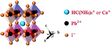
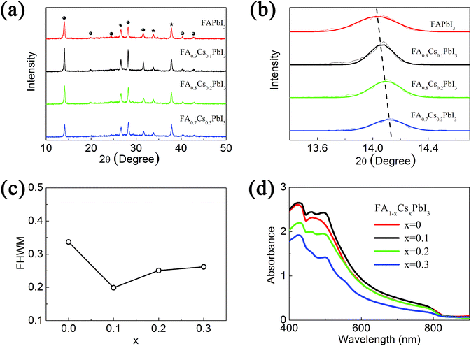
Schematic illustration of the crystal structure of FAPbI3 with Cs+ ions incorporation is shown in Scheme 1. Four kinds of FA1−xCsxPbI3 films (x = 0, 0.1, 0.2 and 0.3) are prepared, and the amounts of Cs+ in the films are confirmed by energy dispersive X-ray spectroscopy (EDS) measurement (Table S1†) and X-ray photoelectron spectroscopy (XPS) measurement (Fig. S5 and Table S2†). Fig. 1(a) is the XRD patterns of these four FA1−xCsxPbI3 films with different Cs+ concentrations. Except three diffraction peaks from the substrate, all diffraction peaks can be assigned to the trigonal crystal structure of FAPbI3 film. It means that our spray reaction method can produce pure α-phase FAPbI3 films at the optimized reaction condition. In Fig. 1(a), the incorporation of Cs+ ions in the FAPbI3 films does not change the XRD patterns of pure α-phase structure. It means that spray reaction method avoids phase separation in the formation of these solid solution films. Fig. 1(b) shows the (110) diffraction peaks of four FA1−xCsxPbI3 films with different Cs+ concentrations. The 2θ angle of diffraction peak increases with the increase of Cs+ concentration. We calculate the lattice parameters of FA1−xCsxPbI3 by the corresponding XRD patterns, which are summarized in Table S3.† It indicates the lattice constant can be modified by controlling the concentration of Cs+ ions, and the more Cs+ ions incorporate the smaller the lattice constant is. This relationship implies that Cs+ ions replace FA+ ions by occupying the A site of AMX3 structure than the interstitial site. And the substitutional solid solution of FA1−xCsxPbI3 can be produced in the Cs+ concentration up to 30% by the spray reaction method. The decrease of lattice constant in the FA1−xCsxPbI3 films is related to relax the extension in the PbI6 matrices. Furthermore, the full width of half maximum (FWHM) of the (110) diffraction peaks in these four films are also different, which is summarized in Fig. 1(c). The FWHM of FAPbI3 film (0.337°) is much larger than that of FA0.9Cs0.1PbI3 (0.199°), while the FWHMs are 0.251° and 0.262° for FA0.8Cs0.2PbI3 and FA0.7Cs0.3PbI3, respectively. The broadening of XRD peaks are usually induced by the low quality of crystallization in the films. Then the smallest FWHM of FA0.9Cs0.1PbI3 film reflects its highest quality among these four kinds of films. The incorporation of Cs+ ions also induces the variation of light absorption as show in Fig. 1(d). The absorption edge blue shifts by increasing Cs+ concentration. The energy band gaps of FA1−xCsxPbI3 films are calculated by the absorption edge according to Kubelka–Munk equation, which are summarized in Fig. S6 and Table S4.† It indicates Cs+ ions incorporation increases the band gap of FA1−xCsxPbI3. It is noted that light absorption intensity is also different for FA1−xCsxPbI3 films with different Cs+ concentrations. Although large Cs+ concentration (FA0.7Cs0.3PbI3) induces remarkable decrease in the absorption intensity, FA1−xCsxPbI3 with small Cs+ concentration (FA0.9Cs0.1PbI3) exhibits higher absorption intensity than FAPbI3 in the wavelength range of 400–800 nm.
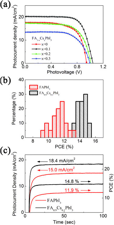
We fabricate perovskite solar cells based on these four kinds of FA1−xCsxPbI3 materials. The photocurrent density–photovoltage characteristics of corresponding devices are shown in Fig. 2(a), and the photovoltaic parameters are summarized in Table 1. By the Cs+ ion incorporation, the short circuit current density (JSC) of corresponding devices increases from 17.7 mA cm−2 at x = 0 to 20.3 mA cm−2 at x = 0.1, whereas further increasing the amount of Cs+ ions decreases JSC to 17.4 mA cm−2 at x = 0.2 and 13.4 mA cm−2 at x = 0.3. Moreover, the open circuit voltage (VOC) is also increased from 0.95 V at x = 0 to 1.05 V at x = 0.1, and then decrease to 1.01 V at x = 0.2 and 0.99 V at x = 0.3. As a result, the PCE of corresponding devices is enhanced from 11.0% to 14.9% by replacing 10% FA+ ions of FAPbI3 with Cs+ ions. The statistics comparison between PCEs of both FAPbI3-based and FA0.9Cs0.1PbI3-based devices is shown in Fig. 2(b). FA0.9Cs0.1PbI3-based devices show an average efficiency of 14.2% with narrow distribution range, which is obviously better than that of FAPbI3-based devices (11.3%). This result indicates that Cs+ ion incorporation can improve the performance of perovskite solar cells based on FAPbI3. We measure the variation of current density with the light soaking time at the constant bias voltage of maximum power condition (Vopt is about 0.8 V). As shown in Fig. 2(c), both FAPbI3-based and FA0.9Cs0.1PbI3-based devices exhibit stabilized power conversion efficiency after 100 seconds light soaking, but the transient time is different. FA0.9Cs0.1PbI3-based device reaches 90% of its stabilized PCE in 3.4 seconds, while FAPbI3-based device needs 8.5 seconds for this transient process. It implies that Cs+ ions incorporation can accelerate to establish the balance state in the devices.
| FA1−xCsxPbI3 | JSC (mA cm−2) | VOC (V) | Fill factor | PCE (%) |
|---|---|---|---|---|
| x = 0 | 17.7 | 0.95 | 0.65 | 11.0 |
| x = 0.1 | 20.3 | 1.05 | 0.70 | 14.9 |
| x = 0.2 | 17.4 | 1.01 | 0.67 | 11.8 |
| x = 0.3 | 13.4 | 0.99 | 0.66 | 8.7 |
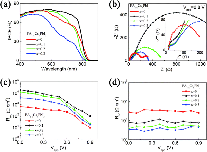
Fig. 3(a) is the incident photon-to-electron conversion efficiency (IPCE) spectra of devices based on FA1−xCsxPbI3 films. At short wavelength range (below 500 nm), all devices based on these four FA1−xCsxPbI3 films exhibit good IPCE values. This can be related to the large absorption coefficient of FA1−xCsxPbI3 films at the short wavelength range. For devices based on FAPbI3, the onset wavelength of IPCE is at 850 nm. After the incorporation of Cs+ ions, the onset wavelength blue shifts to 841 nm, this is in accordance with the blue shifting of absorption edge. It is noted that the onset wavelength of devices based on FA0.9Cs0.1PbI3 films is still obviously longer than that of devices based on MAPbI3 films (at about 800 nm).32 At the middle wavelength range (600 to 700 nm), the IPCE spectra of devices based on these four FA1−xCsxPbI3 films have remarkable different IPCE values. The incorporation of 10% Cs+ ions can increase the IPCE value of corresponding devices, while further increasing the concentration of Cs+ ions leads to the decrease of IPCE value in the middle wavelength range. Although the trend of IPCE value is in accordance with the absorption spectra, the remarkable difference on IPCE values cannot be fully attributed to the minor difference of light absorption. SEM images of FA1−xCsxPbI3 with four different Cs+ ion concentrations are shown in Fig. S7.† Although these FA1−xCsxPbI3 films have similar morphology with compact structure, the grain sizes are different. The grain size distributions are analyzed by Nano Measurer software. The average grain size of FA0.9Cs0.1PbI3 film is 257 nm, which is the largest one in these four samples. As previous reports,7,19 the perovskite film with large crystal grains has improved crystallization and reduced crystal interfaces, which are beneficial to the recombination and transportation process. These improvements can increase the IPCE value of devices. The SEM analysis is accordance with the smallest FHWM of FA0.9Cs0.1PbI3 film in the XRD measurement. We perform impedance spectroscopy (IS) experiments to investigate the recombination and transportation process.
Impedance spectroscopy of perovskite solar cells measured at 0.8 V applied voltage are shown in Fig. 3(b). The obtained impedance data can be fitted with the equivalent circuit (Fig. S8†) to extract the impedance parameters, such as the recombination resistance in the perovskite layer (Rrec) and the charge transfer resistance at the interfaces of selective contacts (Rsc). As previous reports,43–45 the low frequency arc of the impedance spectra can be attributed to the recombination process, and the corresponding resistance (Rrec) is inversely related to the recombination rate of photo-generated electrons. The high frequency arc of the impedance spectra is influenced by the charge transfer resistance at the selective contact layer/perovskite interfaces, and also by the transport resistance in the selective contact layers.43,44 As the selective contact layers do not change in this experiment, the observed differences of high frequency impedance can be attributed to the charge transfer process at the selective contact layer/perovskite interfaces.
Rrec obtained at different applied potentials are summarized in Fig. 3(c). The Rrec with large applied potential is inversely proportion to the recombination rate. It can be observed that the device based on FAPbI3 exhibits the smallest Rrec. The fast recombination leads to the low carrier density, which is accordance with the low open circuit voltage (0.95 V) of the FAPbI3-based device in Fig. 2(a). By incorporation of 10% Cs+ ions in the FAPbI3 films, Rrec increases remarkably and a VOC of 1.05 V is obtained for the corresponding device. Further increasing the concentration of Cs+ ions to 20% and 30%, the Rrec of corresponding devices reduce gradually, which is accordance with the decrease of VOC in Fig. 2(a). The trend of recombination process is also accordance with the quality of crystallization in the corresponding FA1−xCsxPbI3 films in Fig. 1(c). It means that improving the quality of light harvester films is an effective way to decease the recombination rate in the perovskite solar cells.
Fig. 3(d) shows the Rsc obtained at different applied potentials. Rsc almost does not change at various applied potentials, and it decreases with the increase of Cs+ concentration in FA1−xCsxPbI3. It implies that Cs+ incorporation is beneficial for the charge transfer at the selective contact layer/perovskite interfaces. Rsc is related with the series resistance of solar cells, while Rrec at low applied voltage reflects the shunt resistance. Small Rsc and large Rrec lead to good fill factor of solar cells.43 As a result, the fill factor of FAPbI3-based device (0.65) is enhanced to 0.70 by the 10% incorporation of Cs+ ions. Although FA0.8Cs0.2PbI3-based and FA0.7Cs0.3PbI3-based devices have lower Rsc than FA0.9Cs0.1PbI3-based device, the decrease of Rrec at low applied voltage lead to the slightly decrease in fill factor (0.67 and 0.66).
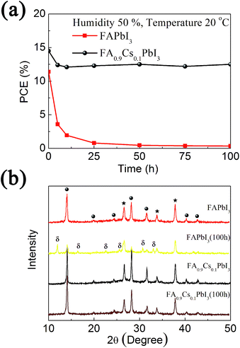
Moreover, the stability of unsealed devices based on FAPbI3 and FA0.9Cs0.1PbI3 films are investigated in the environment of 50% humidity at 20 °C for 100 hours. The PCE decay is summarized in Fig. 4(a). In the first five hours, the PCE of device with FAPbI3 light harvester film decreases from 11.4% to 3.58%. It further decreases to 0.35% after the aging of 100 hours. On the contrary, the PCE of device with FA0.9Cs0.1PbI3 light harvester film decreases from 14.5% to 12.4% in the first five hours, and no obviously change is detected in the following time of 100 hours aging (12.5% at 100 hours). The photographs of these devices with and without aging process are shown in the ESI (Fig. S9†). After 100 hours aging, the FAPbI3-based device becomes yellow in color, while the FA0.9Cs0.1PbI3-based device remains its dark brown color. This result indicates 10% Cs+ ions incorporation leads to remarkable improvement on the humidity stability of devices.
We also age naked FAPbI3 and FA0.9Cs0.1PbI3 films without hole conductor layers and Au electrode layers in the same condition. Fig. 4(b) shows the corresponding XRD patterns of these films before and after the aging process. Before humidity aging, both FAPbI3 and FA0.9Cs0.1PbI3 films give a set of strong peaks, which indicate an α-phase crystal structure of halide perovskite (marked with solid circles). After 100 hours aging, the peaks of δ-phase FAPbI3 appear in the XRD patterns of the FAPbI3 film (marked with δ), and the peaks of α-phase FAPbI3 greatly attenuate. It indicates that most of α-phase FAPbI3 changes into δ-phase FAPbI3 in the aging process. As δ-phase FAPbI3 cannot act as an effective light harvester for perovskite solar cell, the remarkable performance decay of FAPbI3-based device in Fig. 4(a) can be attributed to the damage of α-phase FAPbI3 film. On the contrary, FA0.9Cs0.1PbI3 film still shows strong diffraction peaks of α-phase after the aging process, and no peak for δ-phase is observed. The undamaged FA0.9Cs0.1PbI3 light harvester film leads to the stable performance of device in the aging process. This result indicates the Cs+ ions incorporation can enhance the stability of α-phase structure, which is the major factor for improving the humidity stability of perovskite photovoltaic devices.
Conclusions
In summary, we prepare a series of FA1−xCsxPbI3 solid solution films as the light harvester in perovskite solar cells by the spray reaction method. XRD analysis reflects that solid solution with pure α-phase structure is obtained in the Cs+ concentration up to 30%, and its lattice constant can be adjusted by controlling Cs+ concentration. By optimizing the composition of FA1−xCsxPbI3 films, the average PCE of devices is enhanced from 11.3% for FAPbI3 to 14.2% for FA0.9Cs0.1PbI3. This improvement can be attributed to the increase of light absorption intensity and the decrease of recombination process. Furthermore, FA0.9Cs0.1PbI3 also exhibits better humidity stability than FAPbI3. In the 50% humidity environment, α-phase FAPbI3 rapidly translates into its δ-phase, and the PCE of FAPbI3-based device decreases to 0.35% after the aging of 100 hours. On the contrary, FA0.9Cs0.1PbI3 remains its α-phase structure in the humidity aging process, and the PCE of corresponding device keeps constant at about 12.5% after the initially minor decrease.Acknowledgements
This work was partially supported by National Natural Science Foundation of China (Grant No. 51273079, 11374121), National Basic Research Program of China (Grant No. 2011CB808204), the Science Development Program of JiLin Province (Grant No. 20150519021JH), and the Fundamental Research Funds for Central Universities at Jilin University.Notes and references
- A. Kojima, K. Teshima, Y. Shirai and T. Miyasaka, J. Am. Chem. Soc., 2009, 131, 6050 CrossRef CAS PubMed.
- J. Im, C. Lee, J. Lee, S. Park and N. Park, Nanoscale, 2011, 3, 4088 RSC.
- H. Kim, C. Lee, J. Im, K. Lee, T. Moehl, A. Marchioro, S. Moon, R. Humphry-Baker, J. Yum, J. Moser and M. Grätzel, Sci. Rep., 2012, 2, 591 Search PubMed.
- M. Lee, J. Teuscher, T. Miyasaka, T. Murakami and H. Snaith, Science, 2012, 338, 643 CrossRef CAS PubMed.
- M. Liu, M. Johnston and H. Snaith, Nature, 2013, 501, 395 CrossRef CAS PubMed.
- J. Burschka, N. Pellet, S. Moon, R. Humphry-Baker, P. Gao, M. Nazeeruddin and M. Grätzel, Nature, 2013, 499, 316 CrossRef CAS PubMed.
- J. Im, I. Jang, N. Pellet, M. Grätzel and N. Park, Nat. Nanotechnol., 2014, 9, 927 CrossRef CAS PubMed.
- J. Yan and B. Saunders, RSC Adv., 2014, 4, 43286 RSC.
- Y. Yang, J. Xiao, H. Wei, L. Zhu, D. Li, Y. Luo, H. Wu and Q. Meng, RSC Adv., 2014, 4, 52825 RSC.
- L. Etgar, P. Gao, Z. Xue, Q. Peng, A. Chandiran, B. Liu, M. Nazeeruddin and M. Grätzel, J. Am. Chem. Soc., 2012, 134, 17396 CrossRef CAS PubMed.
- M. Cai, V. Tiong, T. Hreid, J. Bell and H. Wang, J. Mater. Chem. A, 2015, 3, 2784 CAS.
- J. Xiao, J. Shi, H. Liu, Y. Xu, S. Lv, Y. Luo, D. Li, Q. Meng and Y. Li, Adv. Energy Mater., 2015, 5, 1401943 Search PubMed.
- X. Yin, Y. Guo, Z. Xue, P. Xu, M. He and B. Liu, Nano Res., 2015, 8, 1997 CrossRef CAS.
- T. Liu, Q. Hu, J. Wu, K. Chen, L. Zhao, F. Liu, C. Wang, H. Lu, S. Jia, T. Russell, R. Zhu and Q. Gong, Adv. Energy Mater., 2015 DOI:10.1002/aenm.201501890.
- N. Ahn, D. Son, I. Jang, S. Kang, M. Choi and N. Park, J. Am. Chem. Soc., 2015, 137, 8696 CrossRef CAS PubMed.
- H. Zhou, Q. Chen, G. Li, S. Luo, T. Song, H. Duan, Z. Hong, J. You, Y. Liu and Y. Yang, Science, 2014, 345, 542 CrossRef CAS PubMed.
- J. Lee, D. Seol, A. Cho and N. Park, Adv. Mater., 2014, 26, 4991 CrossRef CAS PubMed.
- S. Pang, H. Hu, J. Zhang, S. Lv, Y. Yu, F. Wei, T. Qin, H. Xu, Z. Liu and G. Cui, Chem. Mater., 2014, 26, 1485 CrossRef CAS.
- F. Wang, H. Xu, H. Xu and N. Zhao, Adv. Funct. Mater., 2015, 25, 1120 CrossRef CAS.
- M. Hu, L. Liu, A. Mei, Y. Yang, T. Liu and H. Han, J. Mater. Chem. A, 2014, 2, 17115 CAS.
- D. Seol, J. Lee and N. Park, ChemSusChem, 2015, 8, 2414 CrossRef CAS PubMed.
- G. Eperon, D. Bryant, J. Troughton, S. Stranks, M. Johnston, T. Watson, D. Worsley and H. Snaith, J. Phys. Chem. Lett., 2015, 6, 129 CrossRef CAS PubMed.
- F. Hanusch, E. Wiesenmayer, E. Mankel, A. Binek, P. Angloher, C. Fraunhofer, N. Giesbrecht, J. Feckl, W. Jaegermann, D. Johrendt, T. Bein and P. Docampo, J. Phys. Chem. Lett., 2014, 5, 2791 CrossRef CAS PubMed.
- D. Yuan, A. Gorka, M. Xu, Z. Wang and L. Liao, Phys. Chem. Chem. Phys., 2015, 17, 19745 RSC.
- M. Leyden, M. Lee, S. Raga and Y. Qi, J. Mater. Chem. A, 2015, 3, 16097 CAS.
- S. Aharon, A. Dymshits, A. Rotem and L. Etgar, J. Mater. Chem. A, 2015, 3, 9171 CAS.
- T. Koh, K. Fu, Y. Fang, S. Chen, T. Sum, N. Mathews, S. Mhaisalkar, P. Boix and T. Baikie, J. Phys. Chem. C, 2014, 118, 16458 CAS.
- C. Stoumpos, C. Malliakas and M. Kanatzidis, Inorg. Chem., 2013, 52, 9019 CrossRef CAS PubMed.
- H. Zhang, J. Shi, J. Dong, X. Xu, Y. Luo, D. Li and Q. Meng, J. Energy Chem., 2015, 24, 707 CrossRef.
- G. Eperon, S. Stranks, C. Menelaou, M. Johnston, L. Herz and H. Snaith, Energy Environ. Sci., 2014, 7, 982 CAS.
- N. Pellet, P. Gao, G. Gregori, T. Yang, M. Nazeeruddin, J. Maier and M. Grätzel, Angew. Chem., Int. Ed., 2014, 53, 3151 CrossRef CAS PubMed.
- N. Jeon, J. Noh, W. Yang, Y. Kim, S. Ryu, J. Seo and S. Seok, Nature, 2015, 517, 476 CrossRef CAS PubMed.
- J. Liu, Y. Shirai, X. Yang, Y. Yue, W. Chen, Y. Wu, A. Islam and L. Han, Adv. Mater., 2015, 27, 4918 CrossRef CAS PubMed.
- Y. Chen, T. Chen and L. Dai, Adv. Mater., 2015, 27, 1053 CrossRef CAS PubMed.
- H. Choi, J. Jeong, H. Kim, S. Kim, B. Walker, G. Kim and J. Kim, Nano Energy, 2014, 7, 80 CrossRef CAS.
- C. Bi, Y. Yuan, Y. Fang and J. Huang, Adv. Energy Mater., 2015, 5, 1401616 Search PubMed.
- J. Noh, S. Im, J. Heo, T. Mandal and S. Seok, Nano Lett., 2013, 13, 1764 CrossRef CAS PubMed.
- A. Binek, F. Hanusch, P. Docampo and T. Bein, J. Phys. Chem. Lett., 2015, 6, 1249 CrossRef CAS PubMed.
- W. Yang, J. Noh, N. Jeon, Y. Kim, S. Ryu, J. Seo and S. Seok, Science, 2015, 348, 1234 CrossRef CAS PubMed.
- L. Protesescu, S. Yakunin, M. Bodnarchuk, F. Krieg, R. Caputo, C. Hendon, R. Yang, A. Walsh and M. Kovalenko, Nano Lett., 2015, 15, 3692 CrossRef CAS PubMed.
- Q. Akkerman, V. D'lnnocenzo, S. Accornero, A. Scarpellini, A. Petrozza, M. Prato and L. Manna, J. Am. Chem. Soc., 2015, 137, 10276 CrossRef CAS PubMed.
- X. Xia, H. Li, W. Wu, Y. Li, D. Fei, C. Gao and X. Liu, ACS Appl. Mater. Interfaces, 2015, 7, 16907 CAS.
- E. Juarez-Perez, M. Wuβler, F. Fabregat-Santiago, K. Lakus-Wollny, E. Mankel, T. Mayer, W. Jaegermann and I. Mora-Sero, J. Phys. Chem. Lett., 2014, 5, 680 CrossRef CAS PubMed.
- J. Zhang, E. Juárez-Pérez, I. Mora-Seró, B. Viana and T. Pauporté, J. Mater. Chem. A, 2015, 3, 4909 CAS.
- M. Lv, X. Dong, X. Fang, B. Lin, S. Zhang, X. Xu, J. Ding and N. Yuan, RSC Adv., 2015, 5, 93957 RSC.
Footnote |
| † Electronic supplementary information (ESI) available: Experimental details. See DOI: 10.1039/c5ra23359c |
| This journal is © The Royal Society of Chemistry 2016 |

