
Electrical transport and mechanical properties of thermoelectric tin selenide†
Kriti Tyagiab,
Bhasker Gahtori*a,
Sivaiah Bathulaa,
Niraj Kumar Singha,
Swati Bishnoiab,
S. Aulucka,
A. K. Srivastavaa and
Ajay Dhar*a
aCSIR-Network for Solar Energy, CSIR-National Physical Laboratory, Physics of Energy Harvesting Division, Dr K. S. Krishnan Road, New Delhi-110012, India. E-mail: adhar@nplindia.org; bhasker@nplindia.org; Fax: +91 11 4560 9310; Tel: +91 11 4560 9455 Tel: +91 11 4560 9456
bAcademy of Scientific and Innovative Research (AcSIR), CSIR-NPL Campus, New Delhi-110012, India
First published on 18th January 2016
Abstract
Motivated by the unprecedented thermoelectric performance of SnSe, we report its band structure calculations, based on density functional theory using the full potential linearized augmented plane wave. These calculations were further extended to evaluate the electrical transport properties using Boltzmann transport theory and the results were compared with the as-synthesized polycrystalline counterpart, which was synthesized employing conventional vacuum melting technique followed by consolidation employing spark plasma sintering. The as-synthesized SnSe was thoroughly characterized employing XRD, FESEM and TEM for phase purity, morphology and structure. The theoretically predicted band gap values and the temperature dependence of the electrical transport properties of SnSe were in reasonable agreement with the experimental results, within the approximations employed in our theoretical calculations. These theoretical calculations suggested that the optimum thermoelectric performance in SnSe is expected to occur at a hole doping concentration of ∼3 to 5 × 1021 cm−3. The measured fracture toughness and hardness of SnSe were found to be ∼0.76 ± 0.05 MPa √m and 0.27 ± 0.05 GPa, respectively, which are comparable with other state-of-the-art thermoelectric materials. The high value of thermal shock resistance ∼252 ± 9 W m−1, coupled with its good mechanical properties suggests SnSe to be a potential material for thermoelectric device applications.
1. Introduction
Thermoelectric (TE) materials are currently being vigorously explored as a source of green energy generation from waste-heat.1,2 The thermoelectric figure-of-merit (ZT), which is a material based property, is a direct measure of its thermoelectric performance which is given as1 ZT = (S2σ/κ)T, where S is the Seebeck coefficient, σ is the electrical conductivity and κ the total thermal conductivity. Currently the thrust of thermoelectric research is on developing thermoelectric materials with a high ZT in order to increase the efficiency of their devices so that they can compete with other existing green sources of energy.1,3The anisotropy in TE properties has been well documented on several alloys and compounds and originates primarily due to a variation in their electrical and thermal transport properties when measured along different crystallographic axes.4–6 It manifests itself in terms of different TE performance, when ZT is measured in different directions in a TE sample. This anisotropy in polycrystalline materials mostly arises by using the secondary material processing techniques such as the hot pressing,7,8 spark plasma sintering4,9,10 and extrusion11 of powdered TE material. An example of this kind of large anisotropy has recently been reported in a simple binary compound, SnSe, by Zhao et al.,5 where a vastly different ZT has been observed along the different crystallographic directions. These authors have reported a very high ZT of 2.6 along the b-axis in SnSe single crystals and 2.3 and 0.8 along the c and a-axis, respectively. Although these authors report a large ZT in single crystalline SnSe along its b-axis, but its value in polycrystalline SnSe has been reported to be only 0.3.12
SnSe has a layered structure and crystallizes in orthorhombic symmetry with a space group Pnma (space group no. 63) and undergoes a phase transition above a temperature of 750 K, where it possesses a lower symmetry (Cmcm space group no. 62). Recently, there has been a resurgence in the interest on the TE properties of SnSe5,12–14 ever since Zhao et al.5 reported an unprecedented ZT ∼ 2.62 at 923 K along its b-axis. These authors have experimentally found its electrical and thermal transport properties to be highly anisotropic along all the crystallographic directions. Later, Sassi et al.,14 reported a ZT of 0.5 at 823 K in polycrystalline SnSe, synthesized employing vacuum encapsulation followed by spark plasma sintering. Recently, Chen et al.,12 have reported an enhanced ZT value of 0.6 at 750 K in melt-grown Ag doped polycrystalline SnSe.
Several authors15–19 have reported the band structure of SnSe based on ab initio electronic structure calculations, employing different approximations. He et al.13 have calculated the band structure of SnSe using the generalized gradient approximation (GGA + U) method, as applied in Vienna ab initio Simulation Package (VASP), and reported an indirect band gap of 0.8 eV. Shi and Kioupakis15 have also performed the band structure calculations of SnSe and obtained a gap of 0.829 eV. Employing the first principle calculations using local density approximations (LDA), Kutorasinski et al. have reposted a band gap of 0.465 eV,16 however, Ding et al.17 have obtained a lower band gap of 0.69 eV, calculated using the GGA approximations.
In the present work, we report the theoretically derived electrical transport properties of SnSe, calculated using density functional theory (DFT), which has been compared with those measured experimentally on as-synthesized polycrystalline SnSe. The band structure calculations have been performed using full-potential linearized augmented plane wave (FP-LAPW) as implemented in WIEN2K code, based on DFT and a band gap value of 0.89 for Cmcm-phase has been realized, which is in closest agreement thus far with the reported optical band gap.5,18 The band structure calculations were then extended to theoretically evaluate the electrical transport properties of SnSe, employing the Boltzmann transport theory. The results suggest that the experimentally determined temperature dependent electrical transport behavior agrees well with that predicted theoretically using density-functional theory calculations, employing Engel-Vosko Generalized Gradient Approximation (EVGGA). In addition to the TE performance, the mechanical properties of TE materials are equally important especially during actual device operation. Thus, in the current study, we also report the hardness, fracture toughness and thermal shock resistance of as-synthesized polycrystalline SnSe.
2. Experimental details
Elemental Sn and Se powders supplied by Alfa Aesar, both with a purity of 99.99%, were used as starting materials in this study. Polycrystalline SnSe was synthesized employing conventional vacuum melting process. The Sn and Se powders in a chemical stoichiometric ratio were thoroughly ground in a glove-box under a high-purity argon atmosphere and the resulting powders were subsequently pelletized and vacuum-sealed (10−5 Torr) in quartz tubes. The sealed quartz ampoules were heat-treated at 773 K for 96 h, and then naturally cooled to room temperature. The powders of bulk SnSe were subsequently consolidated and sintered under vacuum (∼4 Pa) using spark plasma sintering (SPS Syntex, 725) at optimized process parameters of pressure 60 MPa and temperature 773 K for 2 min (soaking time) at a heating rate of 200 °C min−1 using graphite die and punches. The density was measured using the conventional Archimedes principle and was found to be 99.2% of the theoretical density. Phase identification and crystallite size measurements were carried out using Rigaku powder XRD (40 kV and 30 mA) and the data was acquired at a scanning speed of 0.51/min with a step width of 0.051. High resolution transmission electron microscopy (HRTEM, model Technai G2 F30 STWIN with a field emission electron gun and operated at 300 kV electron accelerating voltage) was performed on spark plasma sintered (SPS) SnSe. Electrical properties measurements were performed employing ULVAC – ZEM 3 system with an average sample dimensions 2 × 2 × 8 mm. Indentation-crack technique was employed for estimating the fracture toughness using Vickers micro-hardness tester (FM-e7) with a load of 0.98 N for 10 s of indentation time. Field Emission Scanning Electron Microscope (FESEM) – Supra 40VP has been used to study the surface morphology of as-synthesized samples. Fracture tests of the sample have been performed at room temperature using Instron (4204) as per ASTM standard (ASTM: E9-09) with an aspect ratio of ∼2.5 under uniaxial compressive loading with a strain rate of 2 × 10⁻⁵ s−1.3. Computational details
The FP-LAPW19 method in a scalar relativistic version, based on DFT20 as implemented in WIEN2K code, was employed to perform theoretical band structure calculations.21 The atomic coordinates of SnSe were optimized by minimizing the forces acting on each atom. Employing GGA, as given by Perdew–Burke–Ernzerhof,22 we assume that the structure is fully relaxed when the forces on the atoms reach values less than 1 (mRy a.u.−1). Once the forces are minimized in this construction, the self-consistent density at these positions is determined by turning off the relaxations and driving the system to self-consistency. From the relaxed geometry thus obtained, the electronic structure, chemical bonding and electronic charge density were calculated and these were then used to evaluate the transport properties followed by their comparison with the experimentally measured data.The theoretical calculation were performed using the DFT within the FP-LAPW method in a scalar relativistic version as embodied in the WIEN2K code.16,21 The exchange–correlation (XC) potential was solved using three different possible approximations. The XC was described by the LDA and the GGA, which is based on exchange–correlation energy optimization to calculate the total energy.22,23 In addition, we have also used EVGGA,24 which optimizes the corresponding potential for electronic band structure calculations.
It is well-known that in calculating the self-consistent band structure within DFT, the LDA approximation generally underestimates the band gap.25 This is mainly due to the fact that LDA has relatively simple forms that are not sufficiently flexible to accurately reproduce both the exchange–correlation energy and its charge derivative. Engel and Vosko24 considered this shortcoming and constructed a new functional form of GGA that is able to better reproduce the exchange potential at the expense of lesser agreement in with the exchange energy. This approach yields better band splitting and some other properties that mainly depend on the accuracy of the exchange–correlation potential.
The Kohn–Sham equations were solved using a basis of linear augmented plane wave. The potential and charge density in the muffin-tin (MT) spheres are expanded in spherical harmonics with lmax = 10 and non-spherical components up to lmax = 4. We have used RKm = 7.0. In the interstitial region the potential and the charge density are represented by Fourier series. Self-consistency is obtained using 360 k points in the irreducible Brillouin zone (IBZ). The self-consistent calculations converge since the total energy of the system is stable within 0.00001 Ry. We extended our DFT studies to calculate the transport properties using 9900 k points in IBZ, which were calculated employing Boltzmann theory with constant scattering time approximation (CSTA) as implemented in the BoltzTraP code.26–28 The CSTA was used to directly calculate the Seebeck coefficient as a function of doping level and temperature, with no adjustable parameters.29,30
4. Results and discussion
4.1 Microstructural characterization
The X-ray diffraction data of the as-synthesized polycrystalline SnSe sample is shown in Fig. 1(a). The XRD pattern can be indexed to the orthorhombic phase of SnSe and the calculated lattice parameters a = 1.15 nm, b = 0.416 nm, c = 0.443 nm are in good agreement with those reported in the literature.14,31 The sharpness in the peaks in the XRD pattern indicates the highly crystalline behaviour and the absence of other residual peaks in the spectrum exhibits phase purity of the as-synthesized SnSe sample. The average crystallite size of the as-synthesized SnSe was determined using Williamson–Hall method and was found to be ∼42 nm. Fig. 1(b) shows the surface morphology of as-synthesized polycrystalline SnSe, elucidated employing FESEM. It is apparent from the figure that the microstructure exhibits nearly equiaxed nanoscale grains with an average grain size of 40–50 nm, which is in close agreement with that evaluated employing XRD data. Also, the crystallite size distribution graph has been shown in inset of Fig. 1(b).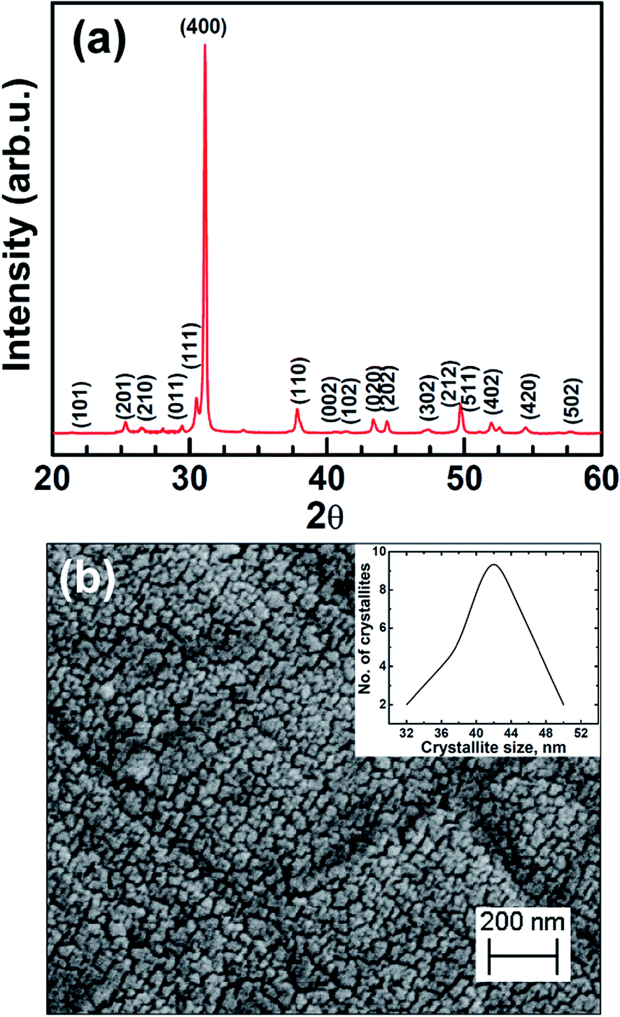 | ||
| Fig. 1 As-synthesized polycrystalline SnSe (a) X-ray diffraction data (b) FESEM micrograph showing inherent nanoscale microstructure. Inset in (b) showing the crystalline size distribution. | ||
A detailed electron microscopy in real and reciprocal space led to important information pertaining to ultra-fine microstructural evolution in the material. Fig. 2(a) shows an illustrative micrograph of fine grains with uniform distribution and densely packed throughout in the microstructure. A corresponding selected area electron diffraction pattern (SAEDP, inset A in Fig. 2(a)) exhibits a polycrystalline nature of the material with the Debye rings, revealing three important atomic planes of the interplanar spacings of 0.293, 0.287, 0.183 nm with respective hkl indices of 111, 400, 511, of an orthorhombic crystal structure (space group: Pnma, lattice parameters: a = 1.15, b = 0.42, c = 0.44 nm, reference: ICDD, 00-014-0159). The ultrafine crystallites of nano-grained microstructure further exhibits that these in most of the instances the thin crystals are overlapping and therefore elucidating the presence of moiré fringes. Inset B in Fig. 2(a) shows a set of almost parallel translational – moiré patterns with a fringe spacing of about 1.13 nm between them. Underneath of these moiré fringes a stacking of high index atomic planes with interplanar spacing of about 0.183 nm (hkl: 511) are also depicted in the inset B of Fig. 2(a). Fig. 2(b) clearly displays that the intrinsically formed individual nanograins are faceted and ultrafine with the size approximately between 30 to 60 nm. At the atomic scale, a grain with size about 40 nm (Fig. 2(b)), shows a distinct stacking of planes with the interplanar spacing of about 0.287 nm of corresponding hkl: 400 (inset C in Fig. 2(b)), in correspondence with XRD and FESEM data. The interfaces between these nanograins were also examined under the electron beam to look into the microstructure. Inset A in Fig. 3 shows an interface (marked with a set of arrows) constituted between the two grains I and II. A further magnified area of encircled region in inset A of Fig. 3 with white dotted line reveal the thickness of the interface about 2 nm stacked between grains I and II (inset B of Fig. 3). Moreover, at the apex of the interface, the microstructure was mixed with the existence of both distorted atomic planes and amorphous phase (inset B of Fig. 3). However the high resolution images of either sides of interface shows single crystalline nature. As an illustrative example, in Fig. 3, a single grain II shows the presence of well stacked atomic planes with the interplanar spacing of 0.293 nm of hkl indices 111.
 | ||
| Fig. 2 HRTEM images of spark plasma sintered SnSe showing (a) ultra-fine distribution of grains, and (b) magnified view of individual grains. Insets: (A) selected area electron diffraction pattern, (B) moiré patterns along with atomic planes, and (C) atomic planes at lattice scale. | ||
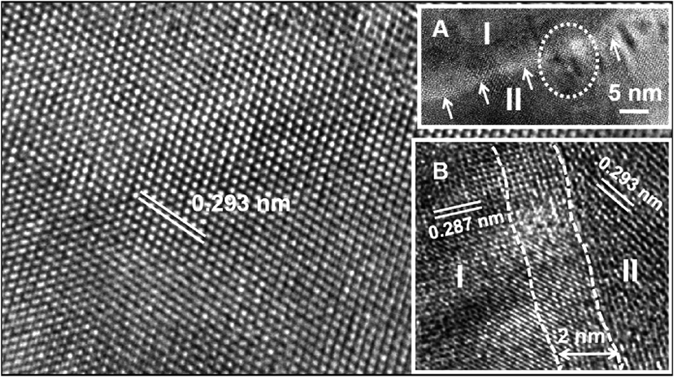 | ||
| Fig. 3 HRTEM images of spark plasma sintered SnSe showing the presence of atomic planes at lattice scale throughout in the microstructure. Insets: (A) interface between grains I and II, and (B) atomic scale image of the same interface as in inset A. | ||
4.2 Band structure calculations
The band structure of SnSe (Cmcm phase), within a few eV from the Fermi level, is shown in Fig. 4(a) (ESI51 Fig. S1(a)† for Pnma phase). The valence band maxima as well as the conduction band minima, along X–Γ direction in the band structure, suggests a direct energy band gap of 0.89 eV, which has also been substantiated experimentally employing UV absorption spectroscopy (ESI51 Fig. S2†). This band gap is in close agreement with that reported earlier from optical absorption measurements (0.898 eV).5,18 The nature of band structure for both the phases of SnSe is similar to that reported by He et al.,13 calculated using VASP. Shi et al.15 have reported a band gap value of 0.829 eV for the Pnma phase, 0.46 eV for the Cmcm phase of SnSe, employing the plane wave pseudo potential model. Kutorasinski et al.16 employed LDA approximation and reported a band gap of 0.465 eV for Pnma and 0.355 eV for Cmcm phase. In yet another study, using the GGA approximation, Ding et al.17 have obtained a band gap of 0.69 eV in Pnma phase, while recently, Zhao et al.5 have reported an indirect band gap of 0.86 eV for the low temperature Pnma phase of SnSe. Thus the band gap values, evaluated in the current study using full-potential WIEN2K code, gives the closest agreement with experimentally determined values, compared to other reported studies.15–18 | ||
| Fig. 4 (a) Electronic band structure for Cmcm-phase of SnSe. The Fermi level is indicated by EF, (b) partial density of states for Cmcm phase of SnSe. Inset shows the magnified view of x-axis of (b) in the energy range from −2 to 2 eV. | ||
Fig. 4(b) shows the contribution of each atom to the density of states (DOS) for the Cmcm phase, via partial-DOS, which clearly shows a finite gap between valance and conduction band (ESI51 Fig. S1(b)† for Pnma phase). The valence band comprises of peaks at around −7.5 eV and between 0 and −5 eV. The peak around −7 eV arises from the s-state of Sn. The top of the valence band has major contributions from Sn-p, Se-p and Sn-s while the bottom of the conduction band arises from Sn-p and Se-p states. We find a significant hybridization between Sn-p, Se-p and Se-d from −5.0 eV to top of valence bands. Conduction band mainly comprises of Sn-p and Se-d states. The inset of Fig. 4(b) shows an enlarged axial view of the partial DOS for Cmcm phase of SnSe, within a few eV from the Fermi level.
4.3 Electrical transport
Fig. 5 shows the temperature dependence of Seebeck coefficient and electrical conductivity of Pnma and Cmcm phases of SnSe along the three crystallographic directions for both hole (p-type) and electron (n-type conduction), calculated using BoltzTrap code,26 over the temperature range of 300–850 K. Hole or electron conduction was obtained by shifting the Fermi level to just below the top of valence band or just above the bottom of conduction band, respectively. It is apparent from these figures that, both, the Seebeck coefficient and electrical conductivity exhibit a strong anisotropy along the three crystallographic axes, for both the phases of SnSe, although, the anisotropy in Seebeck coefficient is comparatively large. These results are in qualitative agreement with the earlier reported experimental5,32 and theoretical studies on SnSe.6,14,15 | ||
| Fig. 5 Temperature dependence of theoretically calculated transport properties along the crystallographic axes for SnSe (a) Seebeck coefficient (b) electrical conductivity and (c) power factor. | ||
Fig. 5(a) shows comparison between the experimentally determined Seebeck coefficient for polycrystalline SnSe with those calculated theoretically along the three crystallographic axes. The experimentally determined positive values of Seebeck coefficient (Fig. 5(a)) indicates a p-type conductivity its temperature dependence is reasonably in close agreement to those calculated theoretically, in the Pnma phase of SnSe. The discontinuity at ∼450 K is accounted to the thermal activation of the carriers5 while at ∼750 K corresponds to the phase transition from Pnma to Cmcm space group.5 This temperature dependence of Seebeck coefficient (Fig. 5(a)) is also similar to those reported experimentally by Sassi et al.14 and Zhao et al.5 However, for Cmcm phase, a mixture of light and heavy conduction bands could explain a nearly temperature independent thermopower owing to bipolar conduction.19
Fig. 5(b) shows that the experimental electrical conductivity increases with temperature although this increase is much sharper in Cmcm phase. In contrast, the theoretically estimated temperature dependence of conductivity of SnSe (p-type) reveals nearly a linear behaviour with a negative slope. This could be attributed to the fact that a constant scattering time (τ) approximation has been used to theoretically evaluate the electrical conductivity using DFT, while in practice τ varies with temperature, hence the observed deviation in experimental and theoretical behaviour of electrical conductivity. Moreover, DFT is known to underestimate the band gap of semiconductors and insulators when using local and semi-local approximation. Hence, SnSe, with a band gap of ∼0.8 eV behaves as metal while performing transport properties calculations using DFT, which is clearly reflected in temperature dependence of electrical conductivity as the theoretically calculated values decrease continuously with temperature in the entire temperature. Despite these limitations, both the calculated and experimental electrical conductivity values lie in same range. In view of various approximations that have been applied in the theoretical calculations, the agreement between experiment and theoretical behaviour of electrical properties of SnSe is quite reasonable. The dependence of power factor (PF) with temperature is also depicted in Fig. 5(c). A strong variation along y-axis as compared to x- and z-axis, in the entire temperature range is observed, which is well in accordance with the results shown in Fig. 5(a) and (b). A slope change at ∼750 K in the experimental results and theoretical calculations indicates the discussed phase transition.
To get a better understanding of the transport phenomenon in SnSe, the Boltzmann transport calculations for the Seebeck coefficient (S), electrical conductivity with respect to relaxation time (σ/τ) and power factor with respect to relaxation time (S2σ/τ) as a function of carrier concentration were carried out. The behaviour of S, σ/τ and S2σ/τ, as a function of carrier concentration, along the three crystallographic axes for both the phases of SnSe, are depicted in Fig. 6(a–f). Fig. 6(a) and (b) show that S decreases with increasing carrier concentration in accordance with the “Pisarenko Relation” for both the phases. This decrease in S, for both Pnma and Cmcm phases, is nearly similar along x- and z-axis however in contrast along the y-axis it shows a lower S till a carrier concentration of ∼2 × 1021 cm−3 after which a broad hump is observed. This suggests that the magnitude of the Seebeck coefficient can be tailored suitably by tuning the carrier concentration. The carrier concentration dependence of σ/τ is shown in Fig. 6(c) and (d) for Pnma and Cmcm phases of SnSe, respectively. These figures suggest that the Cmcm phase exhibits higher values of σ/τ as compared to Pnma phase. Although, while for Pnma phase, σ/τ exhibits almost similar behaviour in all the three crystallographic directions, the anisotropy is clearly pronounced in the case of Cmcm phase. Owing to the different trend in variation of S and σ/τ along the three axis, the S2σ/τ values for Pnma phase show a strong variation with carrier concentration, along all the three axes, as compared to Cmcm phase (Fig. 6(e) and (f)). Typically, in the Pnma phase along y-axis, S2σ/τ value decreases till a carrier concentration of ∼2 × 1021 cm−3 (Fig. 6(e)) after which S starts to increase with temperature (Fig. 6(a)) leading to an overall increase of S2σ/τ values. Similar to S and σ/τ, the graph for S2σ/τ Cmcm phase (Fig. 6(f)) shows a strong variation along y-axis as compared to x- and z-axis, in the entire temperature range. The magnitude of S2σ/τ along y-axis is ∼8 times lower than x- and z-axis. For both the phases, a peak value of S2σ/τ occurs at a carrier concentration of ∼3 to 5 × 1021 cm−3, where the bipolar effect is clearly evident. Fig. 6(f) clearly shows that S2σ/τ would show a maximum value at a hole doping concentration of ∼3 to 5 × 1021 cm−3 which qualifies as an optimum condition for ideal TE performance in Cmcm phase of p-type SnSe.
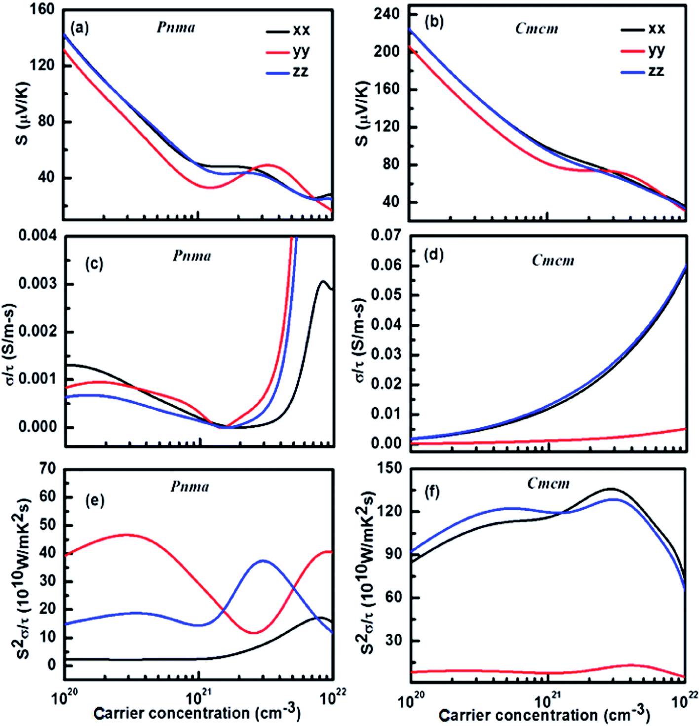 | ||
| Fig. 6 Theoretically calculated carrier concentration dependence of electrical transport coefficients of Pnma and Cmcm-phases of SnSe. (a & b) Seebeck coefficient, (c & d) electrical conductivity with respect to relaxation time (σ/τ) and (e & f) power factor with respect to relaxation time (S2σ/τ). | ||
4.4 Mechanical properties
Most of the research on TE materials has been focused only on their thermal and electrical transport properties,12,29,33–38 primarily aimed towards enhancing their TE performance.9 Nevertheless, their mechanical properties are also equally important the long term durability of the TE devices, as the TE materials, in general, are known to be brittle with low fracture toughness.39 The hardness values of the as-synthesized polycrystalline SnSe, measured using Vickers indentation method at a load of 0.98 N with a dwell time of 10 s, was found to be 0.27 ± 0.05 GPa. The relatively low hardness value of SnSe was attributed to its brittle nature coupled with its bulk to shear modulus ratio which is less than 1.75.13 The fracture toughness (KIC) of brittle materials was estimated using Vicker's indentation-crack technique, given by Antis et al.40 for radial mean crack systems:
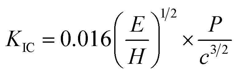 | (1) |
 | (2) |
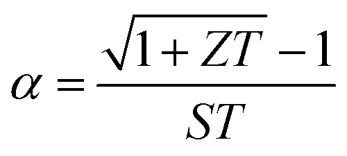
The magnitude of thermal shock resistance for TE materials is very important parameter during actual operation of the device, owing to the temperature gradient between the hot and cold ends of the TE device legs, which can lead to material failure due to internal mechanical stress induced by the temperature gradients.46–48 The thermal shock resistance parameter (RT), is given by the expression,46
 | (3) |
5. Conclusions
The theoretically evaluated temperature dependence of electrical transport properties in SnSe, calculated using first-principle density functional theory and Boltzmann transport equations, have been compared with those measured experimentally on as-synthesized polycrystalline SnSe. These results suggest a reasonable agreement of the theoretically derived band gap and temperature dependence of electrical conductivity and Seebeck coefficient with the experimentally measured values, within the approximations employed in our theoretical calculations. These theoretical calculations suggests that the optimum thermoelectric performance in SnSe is expected to occur at a hole doping concentration of ∼3 to 5 × 1021 cm−3. The mechanical properties of as-synthesized SnSe, including fracture toughness, hardness, fracture strength and thermal shock resistance exhibits values which are comparable to those reported for other state-of-the-art thermoelectric materials.Acknowledgements
This work was supported by CSIR-TAPSUN (CSIR-NWP 54) programme entitled “Novel approaches for solar energy conversion under technologies and products for solar energy utilization through networking”. The authors are grateful to Mr Radhey Shyam and Mr Naval Kishore Upadhyay for the experimental support.References
- D. M. Rowe, Thermoelectrics handbook: macro to nano, CRC press, 2005 Search PubMed.
- G. J. Snyder and E. S. Toberer, Nat. Mater., 2008, 7, 105–114 CrossRef CAS PubMed.
- D. M. Rowe, Modules, systems, and applications in thermoelectrics, CRC Press, 2012 Search PubMed.
- S. D. Bhame, D. Pravarthana, W. Prellier and J. G. Noudem, Appl. Phys. Lett., 2013, 102, 211901 CrossRef.
- L.-D. Zhao, S.-H. Lo, Y. Zhang, H. Sun, G. Tan, C. Uher, C. Wolverton, V. P. Dravid and M. G. Kanatzidis, Nature, 2014, 508, 373–377 CrossRef CAS PubMed.
- A. Hong, L. Li, H. Zhu, Z. Yan, J. Liu and Z. Ren, J. Mater. Chem. A, 2015, 3, 13365–13370 CAS.
- S. R. Brown, S. M. Kauzlarich, F. Gascoin and G. J. Snyder, Chem. Mater., 2006, 18, 1873–1877 CrossRef CAS.
- A. Zevalkink, W. G. Zeier, G. Pomrehn, E. Schechtel, W. Tremel and G. J. Snyder, Energy Environ. Sci., 2012, 5, 9121–9128 CAS.
- K. Biswas, J. He, I. D. Blum, C.-I. Wu, T. P. Hogan, D. N. Seidman, V. P. Dravid and M. G. Kanatzidis, Nature, 2012, 489, 414–418 CrossRef CAS PubMed.
- D. Medlin and G. Snyder, Curr. Opin. Colloid Interface Sci., 2009, 14, 226–235 CrossRef CAS.
- R. Martin-Lopez, A. Dauscher, H. Scherrer, J. Hejtmanek, H. Kenzari and B. Lenoir, Appl. Phys. A: Mater. Sci. Process., 1999, 68, 597–602 CrossRef CAS.
- C.-L. Chen, H. Wang, Y.-Y. Chen, T. Day and G. J. Snyder, J. Mater. Chem. A, 2014, 2, 11171–11176 CAS.
- X. He, H. Shen, W. Wang, Z. Wang, B. Zhang and X. Li, J. Alloys Compd., 2013, 556, 86–93 CrossRef CAS.
- S. Sassi, C. Candolfi, J.-B. Vaney, V. Ohorodniichuk, P. Masschelein, A. Dauscher and B. Lenoir, Appl. Phys. Lett., 2014, 104, 212105 CrossRef.
- G. Shi and E. Kioupakis, J. Appl. Phys., 2015, 117, 065103 CrossRef.
- K. Kutorasinski, B. Wiendlocha, S. Kaprzyk and J. Tobola, Phys. Rev. B: Condens. Matter Mater. Phys., 2015, 91, 205201 CrossRef.
- G. Ding, G. Gao and K. Yao, arXiv preprint arXiv:1505.02477, 2015.
- M. Parenteau and C. Carlone, Phys. Rev. B: Condens. Matter Mater. Phys., 1990, 41, 5227 CrossRef CAS.
- D. J. Singh, Funct. Mater. Lett., 2010, 3, 223–226 CrossRef CAS.
- P. Hohenberg and W. Kohn, Phys. Rev., 1964, 136, B864 CrossRef.
- P. Blaha, K. Schwarz, G. Madsen, D. Kvasnicka and J. Luitz, An augmented plane wave+ local orbitals program for calculating crystal properties, 2001 Search PubMed.
- J. P. Perdew, K. Burke and M. Ernzerhof, Phys. Rev. Lett., 1996, 77, 3865 CrossRef CAS PubMed.
- D. M. Ceperley and B. Alder, Phys. Rev. Lett., 1980, 45, 566 CrossRef CAS.
- E. Engel and S. H. Vosko, Phys. Rev. B: Condens. Matter Mater. Phys., 1993, 47, 13164 CrossRef CAS.
- T. J. Giese and D. M. York, J. Chem. Phys., 2010, 133, 244107 CrossRef PubMed.
- G. K. Madsen and D. J. Singh, Comput. Phys. Commun., 2006, 175, 67–71 CrossRef CAS.
- O. Løvvik and Ø. Prytz, Phys. Rev. B: Condens. Matter Mater. Phys., 2004, 70, 195119 CrossRef.
- L. Hedin and B. I. Lundqvist, J. Phys. C: Solid State Phys., 1971, 4, 2064 CrossRef.
- K. Tyagi, B. Gahtori, S. Bathula, A. Srivastava, A. Shukla, S. Auluck and A. Dhar, J. Mater. Chem. A, 2014, 2, 15829–15835 CAS.
- K. Tyagi, B. Gahtori, S. Bathula, S. Auluck and A. Dhar, Appl. Phys. Lett., 2014, 105, 173905 CrossRef.
- S. Chen, K. Cai and W. Zhao, Phys. B, 2012, 407, 4154–4159 CrossRef CAS.
- X. Guan, P. Lu, L. Wu, L. Han, G. Liu, Y. Song and S. Wang, J. Alloys Compd., 2015, 643, 116–120 CrossRef CAS.
- B. Gahtori, S. Bathula, K. Tyagi, M. Jayasimhadri, A. Srivastava, S. Singh, R. Budhani and A. Dhar, Nano Energy, 2015, 13, 36–46 CrossRef CAS.
- S. Bathula, J. Mula, B. Bhasker, N. K. Singh, K. Tyagi, A. K. Srivastava and A. Dhar, Nanoscale, 2015, 7, 12474–12483 RSC.
- B. Gahtori, S. Bathula, K. Tyagi, M. Jayasimhadri, A. Srivastava, S. Singh, R. Budhani and A. Dhar, Nano Energy, 2015, 13, 36–46 CrossRef CAS.
- S. Bathula, M. Jayasimhadri, B. Gahtori, N. K. Singh, K. Tyagi, A. K. Srivastava and A. Dhar, Nanoscale, 2015, 7, 12474–12483 RSC.
- S. Bathula, M. Jayasimhadri, N. Singh, A. Srivastava, J. Pulikkotil, A. Dhar and R. Budhani, Appl. Phys. Lett., 2012, 101, 213902 CrossRef.
- S. Fan, J. Zhao, J. Guo, Q. Yan, J. Ma and H. H. Hng, Appl. Phys. Lett., 2010, 96, 182104 CrossRef.
- L.-D. Zhao, B.-P. Zhang, J.-F. Li, M. Zhou, W.-S. Liu and J. Liu, J. Alloys Compd., 2008, 455, 259–264 CrossRef CAS.
- G. Anstis, P. Chantikul, B. R. Lawn and D. Marshall, J. Am. Ceram. Soc., 1981, 64, 533–538 CrossRef CAS.
- F. Ren, B. D. Hall, J. E. Ni, E. D. Case, J. Sootsman, M. G. Kanatzidis, E. Lara-Curzio, R. M. Trejo and E. J. Timm, MRS Proceedings, 2007, 1044, 1044-U04-04 CrossRef.
- G. J. Snyder and T. S. Ursell, Phys. Rev. Lett., 2003, 91, 148301 CrossRef PubMed.
- P. H. Ngan, D. V. Christensen, G. J. Snyder, L. T. Hung, S. Linderoth, N. V. Nong and N. Pryds, Phys. Status Solidi A, 2014, 211, 9–17 CrossRef CAS.
- K. Tyagi, B. Gahtori, S. Bathula, M. Jayasimhadri, S. Sharma, N. K. Singh, D. Haranath, A. Srivastava and A. Dhar, Solid State Commun., 2015, 207, 21–25 CrossRef CAS.
- K. Tyagi, B. Gahtori, S. Bathula, V. Toutam, S. Sharma, N. K. Singh and A. Dhar, Appl. Phys. Lett., 2014, 105, 261902 CrossRef.
- J. R. Salvador, J. Yang, A. A. Wereszczak, H. Wang and J. Y. Cho, Sci. Adv. Mater., 2011, 3, 577–586 CrossRef CAS.
- K. Bartholomé, B. Balke, D. Zuckermann, M. Köhne, M. Müller, K. Tarantik and J. König, J. Electron. Mater., 2014, 43, 1775–1781 CrossRef.
- F. Ren, H. Wang, P. A. Menchhofer and J. O. Kiggans, Appl. Phys. Lett., 2013, 103, 221907 CrossRef.
- J. Salvador, J. Yang, X. Shi, H. Wang, A. Wereszczak, H. Kong and C. Uher, Philos. Mag., 2009, 89, 1517–1534 CrossRef CAS.
- S. Bathula, B. Gahtori, M. Jayasimhadri, S. Tripathy, K. Tyagi, A. Srivastava and A. Dhar, Appl. Phys. Lett., 2014, 105, 061902 CrossRef.
- K. Tyagi, B. Gahtori, S. Bathula, N. K. Singh, S. Bishnoi, S. Auluck, A. K. Srivastava and A. Dhar, RSC Adv., 2016 10.1039/c5ra23742d.
Footnote |
| † Electronic supplementary information (ESI) available. See DOI: 10.1039/c5ra23742d |
| This journal is © The Royal Society of Chemistry 2016 |