In situ growth of SnS absorbing layer by reactive sputtering for thin film solar cells
Lianbo Zhaoa,
Yunxiang Dia,
Chang Yanb,
Fangyang Liu*ab,
Zhu Chenga,
Liangxing Jiang a,
Xiaojing Hao*b,
Yanqing Laia and
Jie Lia
aSchool of Metallurgy and Environment, Central South University, Changsha 410083, China. E-mail: liufangyang@csu.edu.cn; Fax: +86 731 88710171; Tel: +86 139 74914406
bAustralian Centre for Advanced Photovoltaics, School of Photovoltaic and Renewable Energy Engineering, University of New South Wales, Sydney 2052, Australia. E-mail: xj.hao@unsw.edu.au; Tel: +61 432 068 410
First published on 18th December 2015
Abstract
The semiconductor SnS is a promising candidate for low cost earth-abundant photovoltaic absorbing layers and presents some interesting challenges in single phase material preparation. An in situ growth process via reactive sputtering was employed in this work to fabricate SnS thin films. The effect of growth temperature on the properties of prepared films was investigated to obtain phase-pure SnS. It is revealed that the films grown at 400 °C presented a single orthorhombic SnS phase with a direct optical band gap of 1.14 eV, a high optical absorption coefficient above 9.0 × 104 cm−1, and a p-type conductivity with a high carrier concentration around 1017 cm−3. The associated device with a structure of ITO/i-ZnO/CdS/SnS/Mo/glass achieves a power conversion efficiency of 0.26%. Based on the TEM characterization, the limiting factors for SnS device performance are revealed and discussed.
1. Introduction
Tin monosulfide (SnS) has increasingly being studied as a promising light absorbing material for low cost solar cells due to its more abundant and cheaper constituent elements and lower toxic nature, compared with commercially available Cu(In,Ga)Se2 and CdTe.1 SnS is an intrinsic p-type semiconductor with a high absorption coefficient of 104 to 105 cm−1 in the visible region, a near-optimal direct band gap of 1.3 eV and indirect band gap of 1.1 eV, and a high free carrier concentration of 1016 cm−3.2,3 These excellent qualities make SnS a very attractive candidate for the fabrication of solar cells on a large scale. So far, the reported highest efficiency of SnS-based thin-film solar cells has achieved 4.63%,4 which is substantially less than the theoretical maximum efficiency around 30% for SnS single-junction devices with a band gap of 1.3 eV according to the detailed balance theory predicted by Shockley–Queisser.5It is generally believed that the poor performance of current SnS solar cells is mainly related to the low quality of SnS films, detrimental impurity phases like Sn2S3 or SnS2,6 and non-optimal device architecture.7,8 Various methods have been investigated for the preparation of high quality SnS films, e.g. chemical vapor deposition (CVD),1,9 atomic layer deposition (ALD),3 thermal evaporation,10–13 sputtering,2,14,15 chemical bath deposition (CBD),16 spray pyrolysis,7,17,18 and electrochemical deposition (ED).19,20 So far most successful methods of fabricating high quality SnS films are related to simultaneous deposition of two elements and crystallization,11,18 such as ALD which produced pure, stoichiometric and homogeneous SnS films from the reaction of bis(N,N′-diisopropylacetamidinato)tin(II) [Sn(MeC(N-iPr)2)2] and H2S at 200 °C and achieved the highest efficiency of 4.63% for SnS-based thin film solar cells.4 However, ALD is a rather slow and expensive method for films fabrication and therefore a direct one-step, high-rate and low-cost deposition process is desperate for large scale production.11 An attractive way that can meet such requirements is reactive sputtering. Sputtering is suitable for the continuous deposition of compound films in large-area, and especially common for oxides and nitrides.21,22 Reactive sputtering can directly provide a homogeneous and crystalline film with tunable composition by adjusting the parameters of sputtering process, such as power, pressure, substrate temperature and H2S/Ar ratio.23 In addition, reactive sputtering has been successfully developed for the deposition of CuInS2 and Cu2ZnSnS4 films,24 with associated devices achieved energy conversion efficiencies of 11.4% and 7.9%, respectively.25,26
In this work, we present a comprehensive exploration of reactive sputtering technique for the in situ growth of SnS thin films. The effects of growth temperature on the structural (including crystal structure, phase, composition, and morphology), optical and electrical properties of the grown films have been investigated. At last, based on SnS films grown by reactive sputtering, the solar cells have been fabricated for the first time and the preliminary performance has been presented.
2. Experimental
The in situ growth of tin sulfide thin films on Mo-coated soda-lime glass substrates was performed by RF reactive sputtering from metal Sn target in Ar/H2S working gas. Simultaneously, soda-lime glasses were also used as substrates for the sake of sulfur content measurement, optical and electrical characterization. The Sn target is 60 mm in diameter and 5 mm in thickness with a purity of 99.99%. The distance between target and substrate was 120 mm and the substrate holder rotated at a frequency of 4 revolutions per minute. The base pressure of the sputtering system was approximately 10−4 Pa. The flow of Ar (purity: 99.999%) and H2S (purity: 99.9%) were 30 sccm and 10 sccm respectively with a total pressure of 0.5 Pa. The sputtering power and time is 80 W and 30 min, respectively. During the deposition, the substrate was heated to the designed growth temperatures, i.e. room temperature (RT), 200 °C, 300 °C and 400 °C, respectively.The surface and cross-sectional morphology of the films were analyzed by scanning electron microscopy (SEM, FEI Quanta-200) combined with an energy dispersive X-ray spectroscopy (EDS, EDAX-GENSIS60S). The film thickness was measured via a combination of cross-sectional SEM and profile meter (Veeco Dektak 150). The crystal structure of the films was analyzed by X-ray diffraction (XRD, Rigaku3014). Raman scattering measurements (LabRAM HR800) were performed at an excitation wavelength of 480 nm. The optical transmittance was recorded by a UV-Vis-near IR spectrophotometer (Hitachi U-4100) in the wavelength range of 300 to 2000 nm. The carrier concentration, carrier mobility and resistivity of the films were measured by the Hall effect measurement (HMS-3000/0.55 T) using the van der Pauw method at 300 K. A FEI Tecnai G2 equipped with energy dispersive spectroscopy (EDS) detector was used for the transmission electron microscopy (TEM) analysis.
Solar cell based on SnS thin films were fabricated by depositing a CdS buffer layer via chemical bath deposition according to the procedure described elsewhere,27 and an i-ZnO/ITO window layer via magnetron sputtering. The solar cell performance was characterized by current–voltage (I–V) measurements using an AM 1.5 solar simulator (NEWPORT, 100 mW cm−2) and a digital source meter (Keithley 2400).
3. Results and discussion
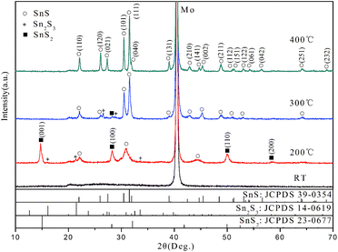
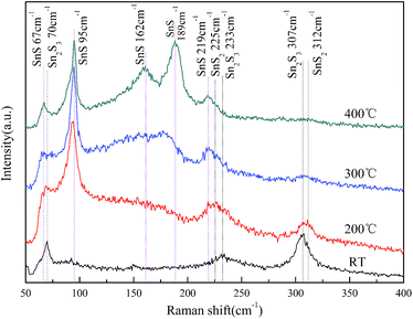
Fig. 1 shows the XRD patterns of the films grown at different temperatures ranging from RT to 400 °C. It is demonstrated that the growth temperature plays a crucial role in determining the phase and purity of films. For the films grown at RT, no obvious diffraction peaks can be observed except for that corresponding to Mo from Mo-coated substrate, which indicate indefinite phase of the film within sensitivity limit of the instrument. As the growth temperature increased to 200 °C, mixed phases including SnS2, Sn2S3 and SnS were presented according to the diffraction patterns. The peaks at 2θ = 14.8, 28.3, 49.9 and 58.5° match the standard pattern of hexagonal SnS2 (JCPDS no. 23-0677). Also trace orthorhombic Sn2S3 phase (JCPDS no. 14-0619) was detected. The broad peak at 2θ = 30.9° should result from the overlap and cross bonding between (101) and (111) peaks of SnS due to the low crystallinity. When the growth temperature increased to 300 °C, the intensity of SnS2 and Sn2S3 peaks decrease greatly and the peaks of SnS become the dominant ones. Only few weak peaks at 2θ = 26.6, 28.9 and 28.3° corresponding to the residual Sn2S3 and SnS2 were observed. Further increasing the growth temperature to 400 °C, the film is highly crystallized and consists of phase-pure SnS within the detection limit of XRD. The XRD feature matches well with orthorhombic structure of SnS (JCPDS no. 39-0354, a = 4.329 Å, b = 11.192 Å, c = 3.984 Å) and shows preferred orientation along (111) plane, which is in agreement with the reported results for SnS thin films grown by other techniques.3,11,28 In general, the crystallinity and SnS phase of deposited films are improved with elevating the growth temperature.Raman scattering measurement has performed to further confirm the phases of films grown at different temperatures and the results are shown in Fig. 2. The films grown at RT show only three band peaks at 70, 233 and 307 cm−1 which match well with the reported spectra of Sn2S3.9 This indicates that Sn2S3 was the main product while SnS was not formed in the RT growth process. The spectrum of the films grown at 200 °C confirms the presence of SnS from the band peaks at 95 and 219 cm−1.9,29 Meanwhile, SnS2 and Sn2S3 were detected in the films due to their characteristic Raman peaks at 312 and 307 cm−1, respectively.9 When it comes to the films grown at 300 °C, the peaks of Sn2S3 and SnS2 reduce in intensity significantly but still remain. The major component turns over to be SnS phase, which agrees well with the aforementioned XRD analysis. The films grown at 400 °C shows the band peaks at 67, 95, 162, 189 and 219 cm−1, which well correspond to the reference spectrum of SnS.3,9 The characteristic peaks from the other secondary phases such as Sn2S3 and SnS2 cannot be observed, which indicate that a phase-pure SnS film was successfully in situ grown by reactive sputtering at 400 °C.
In order to provide further evidence of the phase identities, the ratio of tin to sulfur (Sn![[thin space (1/6-em)]](https://www.rsc.org/images/entities/char_2009.gif) :
:![[thin space (1/6-em)]](https://www.rsc.org/images/entities/char_2009.gif) S) for the films grown at different temperatures was determined by EDS analysis, as shown at Table 1. The results are in good agreement with the structural assignment. The films grown at RT and 200 °C had a Sn
S) for the films grown at different temperatures was determined by EDS analysis, as shown at Table 1. The results are in good agreement with the structural assignment. The films grown at RT and 200 °C had a Sn![[thin space (1/6-em)]](https://www.rsc.org/images/entities/char_2009.gif) :
:![[thin space (1/6-em)]](https://www.rsc.org/images/entities/char_2009.gif) S ratio close to 1
S ratio close to 1![[thin space (1/6-em)]](https://www.rsc.org/images/entities/char_2009.gif) :
:![[thin space (1/6-em)]](https://www.rsc.org/images/entities/char_2009.gif) 1.5, corresponding most closely to Sn2S3 or the mixture of SnS2 and SnS. As the grown temperature increases, the Sn
1.5, corresponding most closely to Sn2S3 or the mixture of SnS2 and SnS. As the grown temperature increases, the Sn![[thin space (1/6-em)]](https://www.rsc.org/images/entities/char_2009.gif) :
:![[thin space (1/6-em)]](https://www.rsc.org/images/entities/char_2009.gif) S ratio increased clearly. Finally, a single phase of SnS was obtained at 400 °C with a slightly sulfur-rich composition of SnS1.02.
S ratio increased clearly. Finally, a single phase of SnS was obtained at 400 °C with a slightly sulfur-rich composition of SnS1.02.
| Tgrow (°C) | RT | 200 | 300 | 400 |
|---|---|---|---|---|
| Phase composition | Sn2S3 | SnS2 + SnS + Sn2S3 (traces) | SnS + SnS2 (traces) + Sn2S3 (traces) | SnS |
| Elemental composition | SnS1.51 | SnS1.52 | SnS1.16 | SnS1.02 |
| Thickness (μm) | 1.00 | 1.40 | 1.25 | 0.87 |
| Eg (eV) | 1.92 | 1.42 | 1.40 | 1.14 |
| n (cm−3) | −3.81 × 10¹¹ | −1.82 × 10¹⁷ | 6.04 × 10¹⁷ | 2.11 × 10¹⁷ |
| μ (cm2 V−1 s−1) | 31.32 | 1.29 | 0.51 | 2.69 |
| ρ (Ω cm) | 6.28 × 10⁵ | 28.59 | 20.61 | 12.83 |
| Type | n | n | p | p |
The SEM images in Fig. 3 show the surface and cross-sectional morphology of the films grown at different temperatures. The film grown at RT shows fairly smooth surface and consists of small grains without any void from surface (Fig. 3(a)) and cross-sectional (Fig. 3(e)) SEM images. The crystalline faces or edges cannot be seen clearly, which implies low crystallinity of the film. As the growth temperature increases, rougher surface and larger grains are observed from Fig. 3(b and c). As it can be seen from the cross-sectional view (Fig. 3(f and g)), lengthy and flaky grains extending the full thickness of the films are observed and the lateral grain size increases obviously, which should be beneficial to the solar cell performance according to the previous experience in CIGS and CZTS thin film solar cells.30,31 When the growth temperature rises to 400 °C, clear and sharp crystal facets appeared on SnS grains (see Fig. 3(d and h)). The above results show that the crystallinity of the films was improved and clearer growth orientation perpendicular to the substrates was observed with increasing growth temperature. It is worth noting that growth temperature has a considerable effect on film thickness which has been analyzed and shown in Table 1. This should be mainly caused by different sulfur content, density and compactness of various tin sulfides, e.g. SnS, Sn2S3 and SnS2 which present in the films grown at different temperatures. Besides, SnS has a high volatility and may be evaporated at high temperature and low pressure, which might be another reason for the thinner film grown at 400 °C.
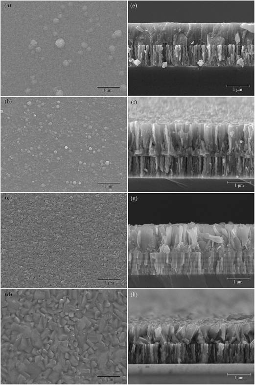 | ||
| Fig. 3 Surface and cross-sectional SEM images of films grown at RT (a and e), 200 °C (b and f), 300 °C (c and g) and 400 °C (d and h). | ||
In order to further confirm the valence states and purity of the film grown at 400 °C, XPS measurements were performed after Ar sputtering for 3 min and the results presented in the Fig. 4. The XPS peaks were calibrated by XPS line of C1s at 284.5 eV. O1s, N1s and C1s were not detected which indicate high purity of reactively sputtered SnS films. The peaks at 485.88 and 494.38 eV correspond to the binding energy of Sn3d5/2 and Sn3d3/2, respectively and the peak splitting of 8.50 eV is consistent with that for Sn in the oxidation state of +2. The S2p peak at 161.46 eV corresponds to that for S in the oxidation state of −2. All the binding energies and peak splitting of the SnS film are in good agreement with the values reported earlier for Sn2+, and S2− in SnS.3,32 Besides, from the XPS results we find that no other valences, such as Sn(VI) could not be detected.
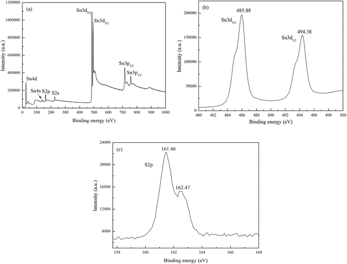 | ||
| Fig. 4 XPS spectra of the films grown at 400 °C, (a) wide scan pattern, (b) Sn3d emission peaks, (c) S2p emission peaks. | ||
The absorption coefficient (α) was determined from the transmittance spectra which were recorded by a UV-Vis-near IR spectrophotometer, as shown in Fig. 5(a). It can be observed clearly that SnS film grown at 400 °C has the highest α above 9.0 × 104 cm−1 in the wavelength of 400 nm to 800 nm, which indicates that only 260 nm is enough for the thickness of SnS film to absorb 90% of the incident photons. According to Tauc et al.,3,33 the optical band gap (Eg) is determined by the calculation
| (αhν)n = A(hν − Eg) | (1) |
 | ||
| Fig. 5 Optical properties of the films grown at different temperatures, (a) α versus hν, (b) a plot of (αhν)2 versus hν corresponding direct band gap transition. | ||
The electrical properties of the films grown at different temperatures were measured by the Hall effect measurement using the van der Pauw method at 300 K and the obtained results are summarized in Table 1. It is observed that the conductivity type of the films changed from n-type to p-type as the growth temperature increases. This phenomenon is related to different stoichiometry and phase of the films grown at different temperatures, as Sn2S3 and SnS2 have been reported as n-type materials37,38 and SnS is a natural p-type semiconductor.3,39 The film grown at RT shows a relative low carrier concentration, which leads to a high resistivity. As the growth temperature increase, the obtained films present high carrier concentration and lower resistivity. The obtained SnS film has a carrier concentration up to 2.11 × 1017 cm−3, which is comparable with that of CIGS device40 and similar to those reported by Yanuar et al.41 and Wangperawong et al.,42 but higher than those found by Sinsermsuksakul et al. (1015 to 1016 cm−3), who reported that low carrier concentrations may be due to native point defects such as Sn2+ vacancies caused by slight deviations from stoichiometry. The mobility is slightly lower than those reported by others.3,41,43 This can be explained by lots of voids between vertical grains causing the decrease of hole mobility along the layer direction.
The SnS film gown at 400 °C was used to fabricate thin film solar cells with the device configuration of ITO/i-ZnO/CdS/SnS/Mo/glass and the active area of cell was 0.15 cm2. As shown in Fig. 6, the J–V characteristic of the cell revealed the efficiency of 0.26% with an open-circuit voltage (Voc) of 162 mV, a short-circuit current density (Jsc) of 6.19 mA cm−2, and a fill factor (FF) of 0.26 was obtained. These performance parameters are much less than those of the record SnS devices.4 It is generally believed that low efficiencies can be due to various reasons, such as bulk material impurities and defects, interface trap states, and notably unfavorable heterojunction band alignment, etc.44–47 To gain insight into the possible reasons for the low efficiency, TEM was used for investigating the cross-section of the SnS solar cell as shown in Fig. 7(a). The presence of long strips of voids is clearly observable in the SnS films. The elemental profiles were determined by EDS scan along the lateral (L1) and vertical (L2) red arrows as shown in Fig. 7(b) and (c), respectively. It is clear that sulfur is homogeneously distributed in the entire area of the film except in the void region. But the intensity of Sn in the surface is relative lower than that in the bulk of SnS film. Besides, Cd was also detected in the surface of SnS film and decreased with the internal extension. This phenomenon is frequently observed in CIGS solar cells and is resulted from the interfacial reaction with an ion exchange between Cd and Cu in the CBD-CdS process.48–50 Furthermore, the presence of pores and voids may accelerate Cd diffusion in the CIGS film.49 Indeed, EDS analysis show that higher concentration of Cd was observed in the void region of SnS absorber layer (see Fig. 7(b)). The band mis-alignment of p-SnS/n-CdS heterojunction leads to large interface recombination due to the “cliff” in the conduction-band offset (Ec,SnS > Ec,CdS).51,52 Theories and experiments suggest that a small positive conduction band offset (CBO) in the range of 0 eV to +0.34 eV is the optimal band alignment for high efficiency solar cells.53–55 That means a material with higher conduction band energy than CdS is preferable for SnS-based thin film solar cells, such as Zn(O,S),46 In2S3,56 (Zn,Cd)S,57 and (Zn,Mg)O.58 Actually, the record high efficiency of 4.63% based on SnS solar cells was achieved by employing Zn(O,S) as the buffer layer.4 Besides, the low conductivity (12.83 Ω cm) of SnS film might be a potential contributor to the poor Voc.54 Also ion-induced defects are common present in the surface of absorber layers grown by sputtering and act as recombination centers.25 A rational surface passivation process could reduce the density of defect states. Gordon et al. reported that recombination near the p-SnS/n-Zn(O,S) junction is reduced by inserting a few monolayers of ALD-SnO2 between these layers.4 Further optimization including increasing the length of minority carrier diffusion, reducing the intrinsic conductivity, improving band-alignment, and passivating the surface defects, etc. is under investigation to boost the efficiency of the reactive sputtering processed SnS thin film solar cells.
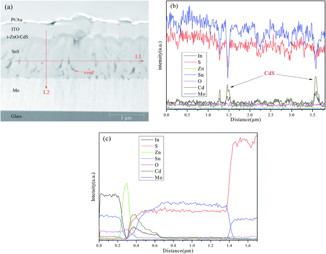 | ||
| Fig. 7 TEM image (a) of device based on SnS film grown at 400 °C, the elemental profiles determined by EDS scan along the lateral (L1) (b) and vertical (L2) (c) red arrow in (a). | ||
4. Conclusions
Tin sulfide thin films were in situ grown by RF reactive sputtering of Sn target in Ar/H2S mixed atmosphere at growth temperatures from RT to 400 °C. Phase-pure SnS has been obtained when the growth temperature reach 400 °C, while Sn2S3 and SnS2 are easier to generate at low growth temperature. As the growth temperature increases, the films show increasingly oriented structure with better crystallinity, the direct band gap decreased from 1.92 to 1.14 eV, and the conduction type changed from n to p-type as well as the resistivity decreased from 6.28 × 10⁵ to 12.83 Ω cm. The suitable optical and electrical properties suggest that the SnS thin film is qualified as a promising absorber material for thin film solar cells. The best solar cell based on the grown SnS films produces a Voc, Jsc and η of 162 mV, 6.19 mA cm−2, and 0.26%, respectively. The deficiencies of SnS and non-optimal device structure may lead to the increase of charge carrier recombination, and therefore limit the cell performance.Acknowledgements
This work was supported by the Fundamental Research Funds for the Central Universities of Central South University (Grant No. 2014zzts031) and the Funds for College Students Innovation Training Project (Grant No. 201410533040).Notes and references
- L. A. Burton, D. Colombara, R. D. Abellon, F. C. Grozema, L. M. Peter, T. J. Savenije, G. Dennler and A. Walsh, Chem. Mater., 2013, 25, 4908–4916 CrossRef CAS.
- K. Hartman, J. L. Johnson, M. I. Bertoni, D. Recht, M. J. Aziz, M. A. Scarpulla and T. Buonassisi, Thin Solid Films, 2011, 519, 7421–7424 CrossRef CAS.
- P. Sinsermsuksakul, J. Heo, W. Noh, A. S. Hock and R. G. Gordon, Adv. Energy Mater., 2011, 1, 1116–1125 CrossRef CAS.
- P. Sinsermsuksakul, L. Sun, S. W. Lee, H. H. Park, S. B. Kim, C. Yang and R. G. Gordon, Adv. Energy Mater., 2014, 4, 1400496 Search PubMed.
- W. Shockley and H. J. Queisser, J. Appl. Phys., 1961, 32, 510–519 CrossRef CAS.
- K. T. Ramakrishna Reddy, P. Purandar Reddy, R. W. Miles and P. K. Datta, Opt. Mater., 2001, 17, 295–298 CrossRef CAS.
- M. Patel and A. Ray, ACS Appl. Mater. Interfaces, 2014, 6, 10099–10106 CAS.
- L. A. Burton and A. Walsh, Appl. Phys. Lett., 2013, 102, 132111 CrossRef.
- L. S. Price, I. P. Parkin, A. M. E. Hardy, R. J. H. Clark, T. G. Hibbert and K. C. Molloy, Chem. Mater., 1999, 11, 1792–1799 CrossRef CAS.
- B. Ghosh, M. Das, P. Banerjee and S. Das, Sol. Energy Mater. Sol. Cells, 2008, 92, 1099–1104 CrossRef CAS.
- V. Steinmann, R. Jaramillo, K. Hartman, R. Chakraborty, R. E. Brandt, J. R. Poindexter, Y. S. Lee, L. Sun, A. Polizzotti, H. H. Park, R. G. Gordon and T. Buonassisi, Adv. Mater., 2014, 26, 7488–7492 CrossRef CAS PubMed.
- H. Noguchi, A. Setiyadi, H. Tanamura, T. Nagatomo and O. Omoto, Sol. Energy Mater. Sol. Cells, 1994, 35, 325–331 CrossRef CAS.
- N. Revathi, S. Bereznev, M. Loorits, J. Raudoja, J. Lehner, J. Gurevits, R. Traksmaa, V. Mikli, E. Mellikov and O. Volobujeva, J. Vac. Sci. Technol., A, 2014, 32, 061506 Search PubMed.
- M. G. Sousa, A. F. da Cunha and P. A. Fernandes, J. Alloys Compd., 2014, 592, 80–85 CrossRef CAS.
- G. P. Wei, Z. L. Zhang, W. M. Zhao, X. H. Gao, W. Q. Chen, H. Tanamura, M. Yamaguchi, H. Noguchi, T. Nagatomo and O. Omoto, Photovoltaic Energy Conversion, IEEE Photovoltaic Specialists Conference, 1994 Search PubMed.
- A. R. Garcia-Angelmo, M. T. S. Nair and P. K. Nair, Solid State Sci., 2014, 30, 26–35 CrossRef CAS.
- M. Calixto-Rodriguez, H. Martinez, A. Sanchez-Juarez, J. Campos-Alvarez, A. Tiburcio-Silver and M. E. Calixto, Thin Solid Films, 2009, 517, 2497–2499 CrossRef CAS.
- K. T. Ramakrishna Reddy, N. Koteswara Reddy and R. W. Miles, Sol. Energy Mater. Sol. Cells, 2006, 90, 3041–3046 CrossRef CAS.
- Z. Zainal, M. Z. Hussein and A. Ghazali, Sol. Energy Mater. Sol. Cells, 1996, 40, 347–357 CrossRef CAS.
- M. Kul, Vacuum, 2014, 107, 213–218 CrossRef CAS.
- P. Frach, D. Gloss, K. Goedicke, M. Fahland and W. M. Gnehr, Thin Solid Films, 2003, 445, 251–258 CrossRef CAS.
- H. C. Barshilia, N. Selvakumar, B. Deepthi and K. S. Rajam, Surf. Coat. Technol., 2006, 201, 2193–2201 CrossRef CAS.
- T. Ericson, T. Kubart, J. J. Scragg and C. Platzer-Björkman, Thin Solid Films, 2012, 520, 7093–7099 CrossRef CAS.
- F. Y. Liu, Y. Li, K. Zhang, B. Wang, C. Yan, Y. Q. Lai, Z. A. Zhang, J. Li and Y. X. Liu, Sol. Energy Mater. Sol. Cells, 2010, 94, 2431–2434 CrossRef CAS.
- T. Unold, I. Sieber and K. Ellmer, Appl. Phys. Lett., 2006, 88, 213502 CrossRef.
- J. J. Scragg, T. Kubart, J. T. Wätjen, T. Ericson, M. K. Linnarsson and C. Platzer-Björkman, Chem. Mater., 2013, 25, 3162–3171 CrossRef CAS.
- F. Liu, Y. Lai, J. Liu, B. Wang, S. Kuang, Z. Zhang, J. Li and Y. Liu, J. Alloys Compd., 2010, 493, 305–308 CrossRef CAS.
- P. D. Antunez, D. A. Torelli, F. Yang, F. A. Rabuffetti, N. S. Lewis and R. L. Brutchey, Chem. Mater., 2014, 26, 5444–5446 CrossRef CAS.
- H. Chandrasekhar, R. Humphreys, U. Zwick and M. Cardona, Phys. Rev. B: Solid State, 1977, 15, 2177–2183 CrossRef CAS.
- M. Gloeckler, J. R. Sites and W. K. Metzger, J. Appl. Phys., 2005, 98, 113704 CrossRef.
- T. K. Todorov, K. B. Reuter and D. B. Mitzi, Adv. Mater., 2010, 22, E156–E159 CrossRef CAS PubMed.
- C. Gao, H. Shen, L. Sun, H. Huang, L. Lu and H. Cai, Mater. Lett., 2010, 64, 2177–2179 CrossRef CAS.
- J. Tauc, R. Grigorovici and A. Vancu, Phys. Status Solidi B, 1966, 15, 627–637 CrossRef CAS.
- M. Khadraoui, N. Benramdane, C. Mathieu, A. Bouzidi, R. Miloua, Z. Kebbab, K. Sahraoui and R. Desfeux, Solid State Commun., 2010, 150, 297–300 CrossRef CAS.
- E. Güneri, F. Göde, B. Boyarbay and C. Gümüş, Mater. Res. Bull., 2012, 47, 3738–3742 CrossRef.
- P. Jain and P. Arun, Thin Solid Films, 2013, 548, 241–246 CrossRef CAS.
- A. Sanchez-Juarez and A. Ortíz, Semicond. Sci. Technol., 2002, 17, 931 CrossRef CAS.
- L. Amalraj, C. Sanjeeviraja and M. Jayachandran, J. Cryst. Growth, 2002, 234, 683–689 CrossRef CAS.
- B. D. Malone, A. Gali and E. Kaxiras, Phys. Chem. Chem. Phys., 2014, 16, 26176–26183 RSC.
- L. Zhang, Q. He, W.-L. Jiang, F.-F. Liu, C.-J. Li and Y. Sun, Sol. Energy Mater. Sol. Cells, 2009, 93, 114–118 CrossRef CAS.
- F. Yanuar, G. El-Haj Moussa, F. Guastavino and C. Llinares, Mediterranean Conference for Environment and Solar, 2000 Search PubMed.
- A. Wangperawong, S. M. Herron, R. R. Runser, C. Hägglund, J. T. Tanskanen, H.-B.-R. Lee, B. M. Clemens and S. F. Bent, Appl. Phys. Lett., 2013, 103, 052105 CrossRef.
- C.-C. Huang, Y.-J. Lin, C.-Y. Chuang, C.-J. Liu and Y.-W. Yang, J. Alloys Compd., 2013, 553, 208–211 CrossRef CAS.
- W. Jaegermann, A. Klein and T. Mayer, Adv. Mater., 2009, 21, 4196–4206 CrossRef CAS.
- M. Sugiyama, K. T. R. Reddy, N. Revathi, Y. Shimamoto and Y. Murata, Thin Solid Films, 2011, 519, 7429–7431 CrossRef CAS.
- L. Sun, R. Haight, P. Sinsermsuksakul, S. Bok Kim, H. H. Park and R. G. Gordon, Appl. Phys. Lett., 2013, 103, 181904 CrossRef.
- A. Schneikart, H. J. Schimper, A. Klein and W. Jaegermann, J. Phys. D: Appl. Phys., 2013, 46, 305109 CrossRef.
- T. Nakada and A. Kunioka, Appl. Phys. Lett., 1999, 74, 2444–2446 CrossRef CAS.
- C. Lei, M. Duch, I. M. Robertson and A. Rockett, J. Appl. Phys., 2010, 108, 114908 CrossRef.
- T. Nakada, Thin Solid Films, 2000, 361–362, 346–352 CrossRef CAS.
- H. H. Park, R. Heasley, L. Sun, V. Steinmann, R. Jaramillo, K. Hartman, R. Chakraborty, P. Sinsermsuksakul, D. Chua, T. Buonassisi and R. G. Gordon, Prog. Photovoltaics, 2014, 23, 901–908 Search PubMed.
- A. Wangperawong, P. C. Hsu, Y. Yee, S. M. Herron, B. M. Clemens, Y. Cui and S. F. Bent, Appl. Phys. Lett., 2014, 105, 173904 CrossRef.
- T. Minemoto, T. Matsui, H. Takakura, Y. Hamakawa, T. Negami, Y. Hashimoto, T. Uenoyama and M. Kitagawa, Sol. Energy Mater. Sol. Cells, 2001, 67, 83–88 CrossRef CAS.
- P. Sinsermsuksakul, K. Hartman, S. Bok Kim, J. Heo, L. Sun, H. Hejin Park, R. Chakraborty, T. Buonassisi and R. G. Gordon, Appl. Phys. Lett., 2013, 102, 053901 CrossRef.
- M. Gloeckler and J. R. Sites, Thin Solid Films, 2005, 480–481, 241–245 CrossRef CAS.
- M. Patel and A. Ray, J. Electron. Mater., 2015, 44, 558–567 CrossRef CAS.
- M. Gunasekaran and M. Ichimura, Sol. Energy Mater. Sol. Cells, 2007, 91, 774–778 CrossRef CAS.
- T. Ikuno, R. Suzuki, K. Kitazumi, N. Takahashi, N. Kato and K. Higuchi, Appl. Phys. Lett., 2013, 102, 19390 CrossRef.
| This journal is © The Royal Society of Chemistry 2016 |

