
Self-formation of thickness tunable Bi2Te3 nanoplates on thin films with enhanced thermoelectric performance
Shuai
Liu
a,
Nan
Peng
ab,
Yu
Bai
b,
Dayan
Ma
a,
Fei
Ma
*a and
Kewei
Xu
*ac
aState Key Laboratory for Mechanical Behavior of Materials, Xi'an Jiaotong University, Xi'an 710049, Shaanxi, China. E-mail: mafei@mail.xjtu.edu.cn; kwxu@mail.xjtu.edu.cn
bSuzhou School of Nano-Science and Nano-Engineering, Xi'an Jiaotong University, Suzhou, 215123, Jiangsu, China
cDepartment of Physics and Opt-electronic Engineering, Xi'an University of Arts and Science, Xi'an 710065, Shaanxi, China
First published on 24th March 2016
Abstract
Bismuth telluride thin films were prepared on flexible substrates by magnetron sputtering and then annealed at different temperatures. Interestingly, single-crystal Bi2Te3 nanoplates emerged on the thin films spontaneously, free of any template or catalyst. The self-formation of nanoplates could be ascribed to thermal stress, and a physical mechanism was proposed accordingly. Thermoelectric measurements illustrated that the electronic conductivity increased with annealing temperature owing to the gradually improved crystallization, but the thermal conductivity decreased as a result of enhanced scattering by the lamellar structure. This improved the figure of merit ZT of the Bi2Te3 thin films by more than 4 times and provided us a new concept to obtain high-performance thermoelectric materials.
1. Introduction
Thermoelectric (TE) materials can convert thermal energy and electrical energy from each other, and exhibit great potential applications in refrigeration and power generation.1–3 The conversion efficiency of thermoelectric materials is depicted by the figure of merit ZT = S2σT/k in which S is the Seebeck coefficient, σ is the electric conductivity, κ is the thermal conductivity, and T is the absolute temperature.4,5 According to the relationship, to improve the conversion efficiency of thermoelectric materials, it is mandatory to improve the electric conductivity σ and the Seebeck coefficient S, but lower the thermal conductivity k. A great number of research studies have demonstrated that the scattering of phonons might be enhanced by reducing the feature size and the dimension of materials, and thus the lattice thermal conductivity kph could be lowered and the Seebeck coefficient would be increased at a given carrier concentration.6–10 For instances, in thin films, the interface and grain boundaries are the main scattering centers, and commonly the grain size decreases with reducing film thickness. Hence, the scattering of phonons must be substantially enhanced if the films are thinned. In fact, the enhancement has also been evidenced in other low-dimensional materials11–16 as well as super-lattice systems.17 However, as well known, the electric conductivity is closely related with thermal conductivity. Once the scattering to phonons is enhanced, the scattering to electrons might also be increased and the electric conductivity will be decreased, which is detrimental to the figure of merit ZT. Therefore, how to substantially reduce the thermal conductivity but improve or at least keep the electric conductivity simultaneously is crucial to enhance the thermoelectric performance.Bismuth telluride (Bi2Te3) and derived alloys are suggested as the best thermoelectric materials at near room temperature.18–22 Magnetron co-sputtering,23 electro-deposition,24 pulsed laser deposition,25 organic chemical vapor deposition (MOCVD),26 and molecular beam epitaxy (MBE)27 have been used to fabricate Bi2Te3 thin films. Among them, magnetron co-sputtering has attracted much more attention because of some advantages, such as, exact control on the stoichiometry of thin films, industrially friendly and low cost features. It has been demonstrated that the thermoelectric properties of Bi2Te3 thin films depend on the crystallinity, grain size and crystal orientation.28–30 However, it is still a challenge to reduce the thermal conductivity but improve the electric conductivity of Bi2Te3 thin films simultaneously, as aforementioned above.
In this paper, Bi2Te3 thin films are prepared on flexible substrates by magnetron sputtering and then annealed at the temperatures from 373 K to 473 K for 6 hours. X-ray diffraction (XRD), scanning electron microscopy (SEM) with energy dispersive X-ray spectroscopy (EDX), high resolution transmission electron microscopy (HRTEM), Raman spectra and X-ray photoelectron spectroscopy (XPS) are adopted to characterize the microstructure. It is found that single-crystal Bi2Te3 nanoplates are generated on the thin films spontaneously free of any template or catalyst. The electrical conductivity, Seebeck coefficient and thermal conductivity of the thin films are measured. To be excited, the electronic conductivity increases with annealing temperature, but the thermal conductivity decreases. This improves the figure of merit ZT of Bi2Te3 thin films more than 4 times. The formation mechanism of Bi2Te3 nanoplates and the enhancement on thermoelectric properties is discussed.
2. Experimental details
Bi2Te3 thin films were deposited on flexible polyimide substrates by magnetron co-sputtering of Bi and Te targets (99.99% in purity) at room temperature. Prior to deposition, the polyimide substrates were cleaned ultrasonically in ethyl alcohol and deionized water to remove the pollutant on surface. The deposition chamber was pumped down to a pressure lower than 1 × 10⁻⁴ Pa. The working pressure during deposition was 0.1 Pa with 20 sccm of Ar as the sputtering gas. Radio frequency (RF) powers of 15 W and 20 W were applied for the sputtering of Bi and Te targets, respectively, in order to ensure the stoichiometric ratio of Bi![[thin space (1/6-em)]](https://www.rsc.org/images/entities/char_2009.gif) :Te in 2:3. The distance between the target and substrate was 40 cm, and the substrate holder was rotated at a speed of 100 rpm min−1 to produce homogeneous thin films. The film thickness was about 500 nm. After deposition, the thin films were annealed at the temperatures in the range of 373–473 K for 6 h at a pressure of 10−3 Pa.
:Te in 2:3. The distance between the target and substrate was 40 cm, and the substrate holder was rotated at a speed of 100 rpm min−1 to produce homogeneous thin films. The film thickness was about 500 nm. After deposition, the thin films were annealed at the temperatures in the range of 373–473 K for 6 h at a pressure of 10−3 Pa.
X-ray diffraction (XRD; Bruker D8 Advance) using Cu Kα radiation (λ = 0.1540 nm) was used to characterize the crystal structure in thin films. Field emission scanning electron microscopy (FESEM, Quanta ×50 FEG) and high resolution transmission electron microscopy (HRTEM, JEM-2100F) with Electron Dispersive Spectrometer (EDS) were employed to observe the morphology and analyze the composition of the samples. X-ray photoelectron spectroscopy (XPS, PHI 5700 ESCA) was measured with an excitation source of Al Kα = 1486.6 eV. Raman spectra (Horiba Jobin Yvon Co. Ltd) were measured using a 352 nm laser at a power of 0.5 mW. The Seebeck coefficient was measured by Physical Property Measurement System (PPMS, Quantum Design PPMS-9) and, the electrical properties were measured by Thermoelectric Transport System (Mini CFM MS-5Tesla-THT, Cryogenic Limited of UK). Four-wire method was adopted here. The wires marked by I+ and I− are the heating and cooling sides, respectively. The Seebeck voltage ΔV and temperature difference ΔT were measured between V+ and V− electrodes. The Seebeck coefficient is obtained by ΔV/ΔT. Since the polyimide substrates are insulator for both electric and thermal transport, the influence of the substrates on thermoelectric properties can be avoided. The 3ω analysis was applied to examine the cross-plane thermal conductivity of the prepared Bi2Te3 thin films was measured at room temperature.31–33 The measurement was performed at 300 K in vacuum chamber (10−3 Pa).
3. Result and discussion
Fig. 1(a) shows the XRD patterns of the Bi2Te3 thin films as deposited as well as those annealed at temperatures of 373 K, 423 K and 473 K for 6 h. Nearly no XRD peaks of Bi2Te3 but a weak peak corresponding to Bi (012) plane can be identified at 27.18° in the as-deposited thin films, characteristic of Bi nano-grains embedded in amorphous Bi2Te3 matrix. Since the XRD peak of Te (101) plane is located at 27.56° (PDF#36-1452), extremely close to those of Bi (012) and Bi2Te3 (015) planes, the peaks of Te nano-grains if any cannot be resolved from the spectra. When the thin films are annealed at 373 K, some diffraction peaks of rhombohedral Bi2Te3 emerge (JCPDS card 08-0021), in particular, the peak of Bi2Te3 (015) planes is enhanced, indicating crystallization to some degree. As the annealing temperature is elevated, more diffraction peaks emerge and become stronger, that is, the crystallinity of the thin films is improved substantially, and (015) is the preferred orientation. Fig. 1(b) shows the XRD peaks in a diffraction angle range of 25–30°. Apparently, as compared to the as-deposited sample, the peaks are slightly shifted to higher angle upon thermal annealing. This is mainly due to the densification of atoms in the process from an amorphous structure to a crystalline structure. Since the coefficient of thermal expansion of the polyimide substrate (2.0 × 10⁻⁵ per K)34 is smaller than that of Bi2Te3 (5.08 × 10⁻⁵ per K),35 a compressive thermal stress will be induced in the Bi2Te3 thin films because of smaller expansion of polyimide substrates during the heating process. Hence, the lattice will be further reduced. If the compressive stress is large enough, it might be released through bending or other ways. So the peaks shift slightly to a lower angle at 423 K and 476 K.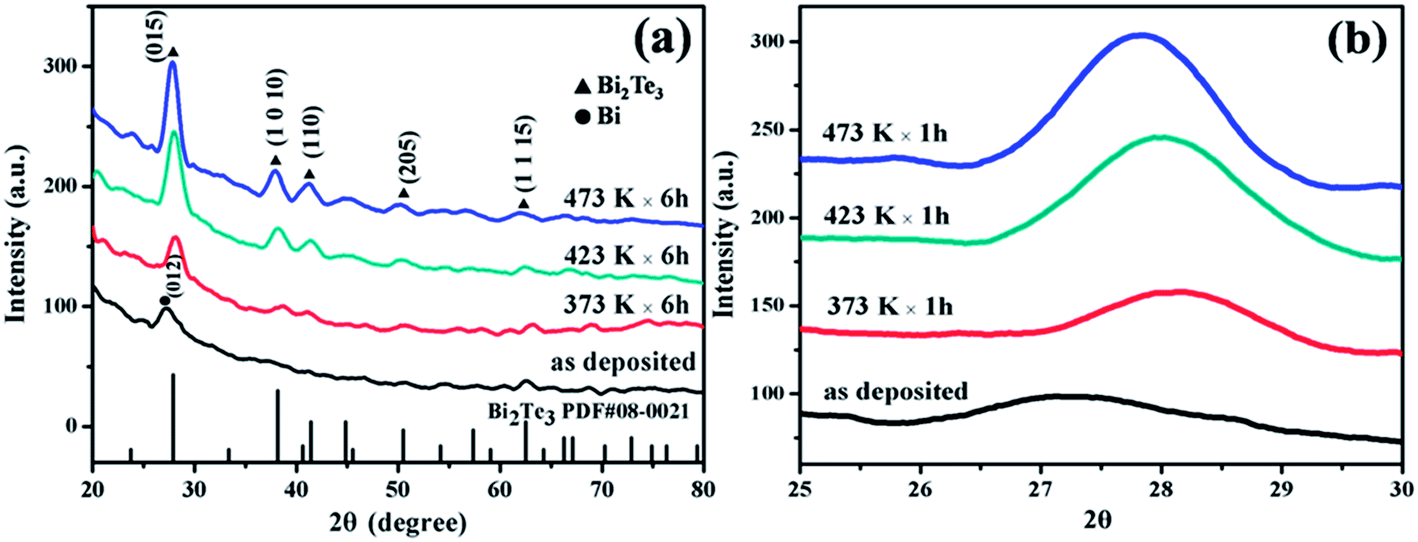 | ||
| Fig. 1 (a) XRD patterns of the as-deposited Bi2Te3 thin films and those annealed at different temperatures; (b) the magnified (015) peak of Bi2Te3. | ||
Fig. 2 shows the chemical composition of the Bi2Te3 thin films evaluated by XPS. Excess Te atoms exist in the as-deposited thin films, but they are evaporated during annealing process. As an example, Fig. 2(a) and (b) exhibit the high-resolution XPS spectra of Bi 4f and Te 3d orbitals in the thin films as-deposited as well as those annealed at 473 K for 6 h. The peak of C 1s at 284.5 eV is used to calibrate the peak positions. The Bi 4f and Te 3d peaks are fitted by the Gaussian method. As compared to the as-deposited thin films, the shape of the XPS spectra of the thin films after thermal annealing changes slightly. Commonly, the peaks at 582.5 eV and 572.0 eV is due to Te 3d3/2 and Te 3d5/2 orbitals in Bi2Te3, and the peaks at 576 eV and 586 eV from Te 3d orbital in tellurium oxidized on surface.36 The XPS spectra of Bi 4f5/2 can be fitted into two sub-peaks at 162.8 eV and 163.8 eV, while that of Bi 4f7/2 be fitted into two ones at 157.5 eV and 158.2 eV. The peaks at 163.8 eV and 158.2 eV are ascribed to bismuth oxide on surface.37 According to the changed ratio of sub-peaks, it is found that the proportion of bismuth oxide increased slightly upon thermal annealing. Hence, a little oxidation occurs on the surface during thermal annealing. Both the XPS and XRD results demonstrate that Bi2Te3 is successfully synthesized. Fig. 3 shows the atomic ratio of Te and Bi in the thin films as deposited and those annealed at different temperatures. It is found that the atomic ratio of Te and Bi decreased from 1.65 in the as-deposited thin films to 1.44 in the thin films annealed at 473 K owing to the evaporation of Te during thermal annealing. The thin films annealed at 423 K for 6 h is nearly stoichiometric of Bi2Te3 (1.48).
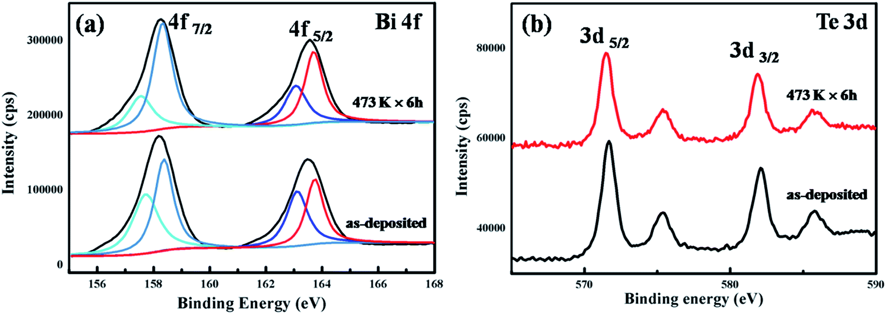 | ||
| Fig. 2 XPS spectra of the as-deposited Bi2Te3 thin films and that annealed at 473 K for 6 h: (a) Bi 4f and (b) Te 3d. | ||
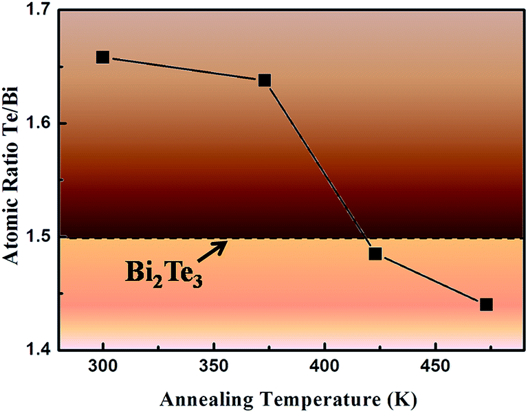 | ||
| Fig. 3 Te/Bi ratios in bismuth telluride films as a function of annealing temperature. | ||
Fig. 4 illustrates the SEM images of surface morphologies of the samples. The surface of the as-deposited Bi2Te3 thin film is smooth decorated with small particles. Upon annealing at 373 K for 6 h, nanoplates emerge on the Bi2Te3 thin films. As the annealing temperature is elevated, the density of nano-plates is increased, the separation between nano-plates is reduced, and the thickness of nano-plates is increased slightly. As shown in the insets of Fig. 4(c) and (d), the thickness of the nanoplates is in the range of 20–40 nm, dependent on the annealing temperature. The formation of nano-plates is driven by the coupling effect of thermal compressive stress and the thermal controlled kinetics. Fig. 5(a) and (b) display the SEM images of the cross-section morphologies of Bi2Te3 thin films. Cracks on the films are produced in preparation of the cross-section samples. Interestingly, it can be found that some nano-plates lie flat on the films, and some are grown out of the thin films [Fig. 5(a)]. The EDX spectrum on the nano-plate reveals that it is stoichiometric Bi2Te3, as illustrated in the inset of Fig. 5(b). The nanoplates are scraped from the films for TEM characterization and, as shown in Fig. 5(c), the nano-plates have polygonal morphologies. The SAED (Selected Area Electron Diffraction) pattern in the inset is characteristic of single-crystal nano-plates. The HR-TEM image in Fig. 5(d) clearly shows that the lattice fringes are uniform with a spacing of 0.690 nm, which is in good agreement with (1010) interplanar distances of rhombohedral Bi2Te3. It also confirms that the nano-plates are highly crystalline.
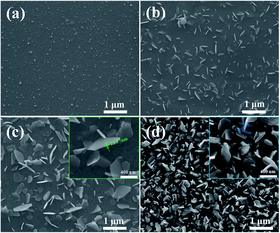 | ||
| Fig. 4 SEM images of surface morphologies of the Bi2Te3 thin films: (a) as-deposited; (b–d) annealed at 373 K, 423 K, and 473 K for 6 h. | ||
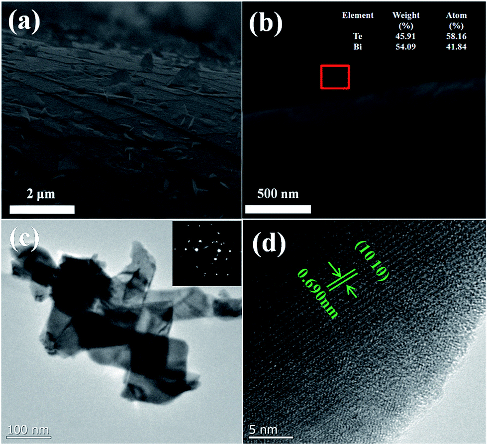 | ||
| Fig. 5 (a and b) Cross-sectional SEM images of Bi2Te3 thin films annealed at 423 K for 6 h, the EDS data of the nanoplates are presented in the inset of panel (b); (c) a low-magnification TEM image and the SAED pattern of Bi2Te3 nanoplates from the films; (d) HRTEM image of a Bi2Te3 nanoplate. | ||
Raman spectra of the thin films as deposited and those annealed at different temperatures are measured in the low frequency region (50–200 cm−1). It is excited by a laser with wavelength of 633 nm (1.96 eV), and the laser power is limited to 0.2 mW to prevent overheating. Fig. 6 shows the results. Two peaks at 121 cm−1 and 138 cm−1 can be identified in samples after thermal annealing, characteristic of the lattice vibration of Bi2Te3. The peak at 121 cm−1 is due to the lattice vibration in A1u mode, in which longitudinal optical phonons at the boundaries of Brillouin zone will be activated.38,39 The A1u peak can usually be observed in the nano-plates owing to the inversion lattice symmetry of Bi2Te3. The peak at 138 cm−1 is due to the lattice vibration in A21g mode, in which the atoms vibrate along the trigonal C axis of Bi–Te quintuple layers, as shown in the inset of Fig. 6. The appearance of both A21g and A1u peaks is ascribed to the broken crystal symmetry in the nano-plates. The gradually increased intensity of Raman peaks at higher annealing temperature on the other hand confirms the increased nano-plates, as observed in SEM images.
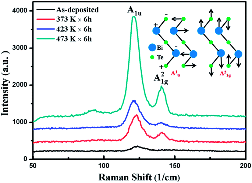 | ||
| Fig. 6 Raman spectra of Bi2Te3 thin films. The displacement vectors of A1u and A21g phonon modes are schematically shown in the inset. | ||
The mechanism for the formation of nanoplates is schematically displayed in Fig. 7(a)–(d). As aforementioned, the thermal expansion coefficient of Bi2Te3 is larger than that of polyimide substrates, compressive stress will be induced in the Bi2Te3 thin films. As compared with the diffusion of vacancies in the lattice, the diffusion rate of Bi and Te atoms along the grain boundaries is higher.7 The thermal induced compressive stress promotes the diffusion of Bi and Te atoms along the grain boundaries in the thin films onto surface. This leads to the formation of Bi2Te3 nanoplates and the compressive stress is released to some degree.40
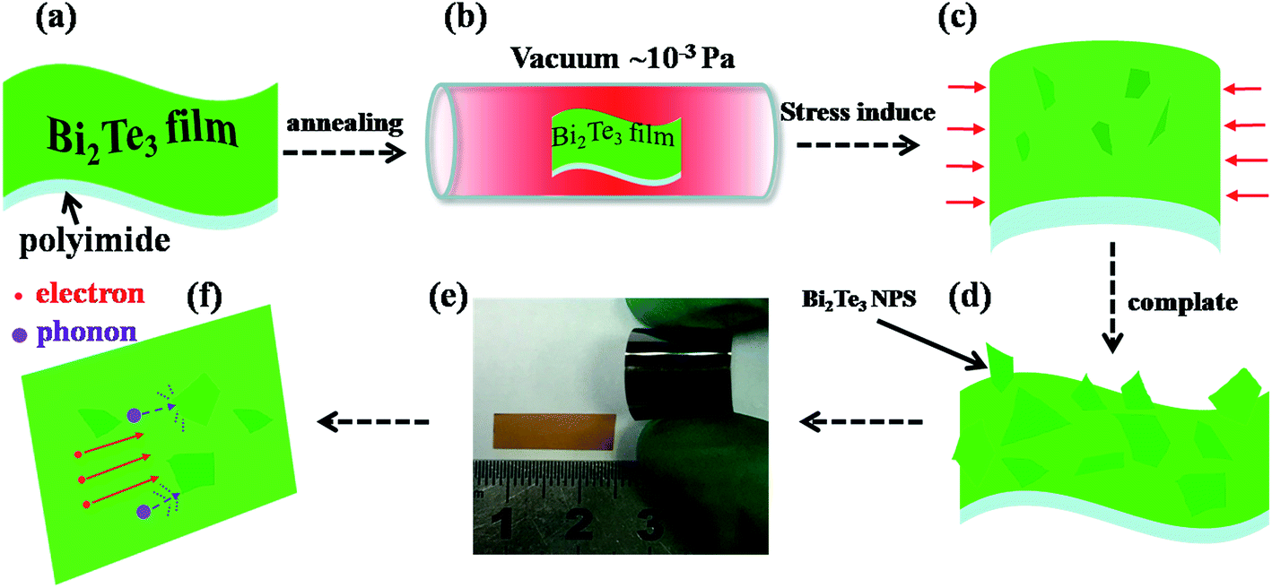 | ||
| Fig. 7 (a–d) Schematic illustration of the fabrication procedure of bismuth telluride film on polyimide substrate and the formation of nanoplates; (e) the photograph of the as-fabricated thin films on highly flexible polyimide substrate; (f) the mechanism of phonon scattering and electron transport on the thin films. | ||
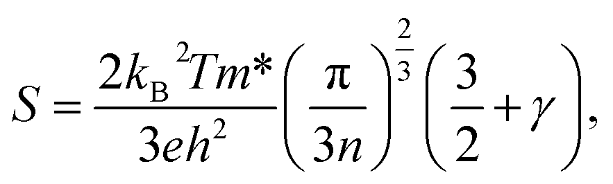
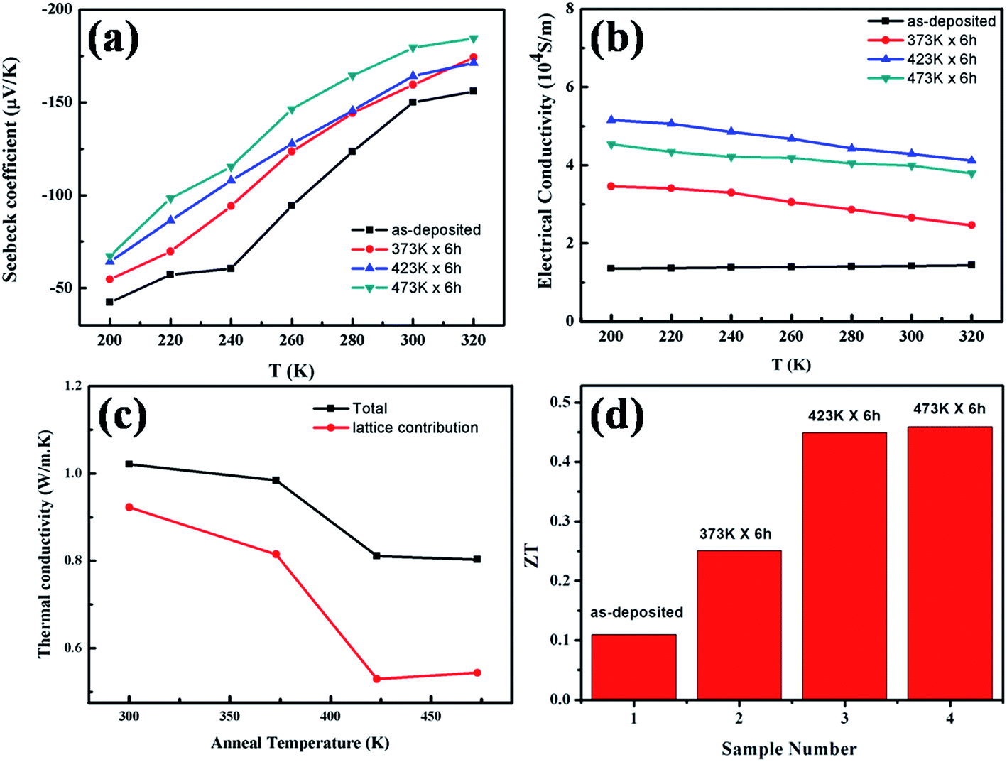
Van Der Pauw method is adopted to measure the electric conductivity of the thin films in the temperature range of 200–320 K and four-wire method is used to measure the Seebeck coefficients, as described above. The thermal conductivities are measured by laser flash method at the room temperature. Fig. 8 presents the measured transport properties of the thin films. As shown in Fig. 8(a), the Seebeck coefficient is negative for all the samples in the temperature measurement range, characteristic of n-type semiconductor of the Bi2Te3 thin films, that is, the major charge carriers are electrons. The absolute values of the Seebeck coefficient in both the as-deposited and thermally annealed samples increase with the increasing temperature almost linearly from 200 K to 320 K. As a whole, the absolute value of the Seebeck coefficient of the as-deposited thin films is the smallest, and it increases with elevating annealing temperature. The Seebeck coefficient of the degenerate semiconductors can be expressed as:41
 | (1) |
 | ||
| Fig. 8 Temperature dependent thermoelectric properties of the thin films: (a) electrical conductivity; (b) Seebeck coefficient; (c) thermal conductivity; (d) ZT values at room-temperature as a function of annealing temperature. | ||
Fig. 8(b) shows the electric conductivity of the samples. As the measurement temperature is elevated, the electrical conductivity of the as-deposited thin films changes little, but those of the annealed thin films decrease, which is the same as what is observed in bulk Bi2Te3, characteristic of degenerate semiconductors.43,44 Although thermal annealing could reduce the defect density and promote the grain growth, the increased scattering to carriers by the enhanced lattice vibration at higher measurement temperature would lower the electric conductivity slightly. The room-temperature electric conductivity of the as-deposited thin films is 1.7 × 10⁴ S m−1, and is increased up to 4.4 × 10⁴ S m−1 when the thin films are thermally annealed at 473 K for 6 h. The increased electric conductivity is attributed to the improved crystallization, as evidenced in XRD patterns.
Thermal conductivity k is contributed by the phonons and electrons, and they are denoted as kL and ke, respectively. ke can be calculated by using the Wiedemann–Franz law, ke = LoσT,45 where Lo is the Lorentz number (2.44 × 10⁻⁸ W Ω K−2 for degenerate semiconductors), σ is the electrical conductivity and T is the absolute temperature. Fig. 8(c) shows the total thermal conductivity k and the contribution by phonons, kL at room temperature. The thermal conductivities of the thin films are significantly smaller than that of bulk Bi2Te3 reported before (2.08 W m−1 K−1).35 The thin films annealed at 473 K for 6 h have the lowest room-temperature thermal conductivity of 0.80 W m−1 K−1, it is lowered by 21% as compared to that of as-deposited thin film (1.02 W m−1 K−1). In fact, the reduction in kL is more remarkable as a result of enhanced scattering to phonons by the surface and interface of the self-formed nano-plates on thin film after thermal annealing. Fig. 7(f) schematically shows the scattering mechanism of phonons. The green solid sheets represent the Bi2Te3 thin film and self-formed nano-plates, the violet balls represent the phonons. As well known, the mean free path of phonons in Bi2Te3 is in the range of 40–60 nm, while that of electrons is one order of magnitude lower than the value. When the phonons are transported on the rough surfaces of Bi2Te3 thin films decorated by nano-plates, multiple collisions should take place,46,47 and the scattering will be enhanced considerably. However, the self-formed nano-plates hardly affect the transport of electrons because the mean free path of electrons in Bi2Te3 is much shorter than the feature sizes of nano-plates. As a result, the figure of merit ZT of Bi2Te3 thin films at room temperature is significantly improved upon thermal annealing, and increases with annealing temperature, as shown in Fig. 8(d). Particularly, the room temperature ZT value of the samples annealed at 473 K has the highest value of 0.45 which is 4 times larger than that of the as-deposited thin films.
As well known, it is difficult to measure the out-of-plane Seebeck coefficient, electrical conductivity, and in-plane thermal conductivity in thin films, so the in-plane Seebeck coefficient, electrical conductivity and the out-of-plane thermal conductivity are measured to evaluate the thermoelectric properties of Bi2Te3 thin films. It is reported that the Seebeck coefficient even in single-crystal Bi2Te3 alloys is almost isotropic since it is sensitive to the band structure near Fermi level but nearly independent on the orientation.48 Therefore, the preferential (015) plane in the annealed thin films has a negligible influence on the Seebeck coefficient. However, different from the Seebeck coefficient, the electrical and thermal transports are anisotropic owing to the orientation dependent mobility of electrons and group velocity of phonons.49 As reported previously, for (015) textured polycrystalline n-type Bi2Te3, the in-plane electrical conductivity at room temperature is about 143% of that along out-of-plane direction,50 while the out-of-plane thermal conductivity is approximately 125% of that along in-plane direction.48 Hence, the ZT value might be overestimated by 14% in this work. But the results are also valuable to study the influence of composition, microstructure and morphology on the thermoelectric properties, now that the same measurement configuration is adopted for all the samples.
4. Conclusion
In this paper, Bi2Te3 thin films were prepared on flexible substrates by magnetron sputtering and then annealed at different temperatures. Since the thermal expansion coefficient of Bi2Te3 is larger than that of polyimide substrates, a compressive stress was produced in the Bi2Te3 thin films. The thermal induced compressive stress promoted the diffusion of Bi and Te atoms along the grain boundaries in the thin films onto surface. This resulted in the formation of Bi2Te3 nanoplates with tunable thickness. A physical mechanism was proposed to understand the process. Thermoelectric property measurement demonstrated that the electronic conductivity increased with annealing temperature owing to the improved crystallization. However, the thermal conductivity was lowered because of the enhanced scattering of phonons by the surface and interface of the self-formed nano-plates. Thus the room temperature ZT value was improved by 4 times. This provides a new way to obtain high-performance thermoelectric materials.Acknowledgements
This work was jointly supported by Key Project of Chinese National Programs for Fundamental Research and Development (Grant No. 2010CB631002), National Natural Science Foundation of China (Grant No. 51271139, 51471130, 51171145, 51302162), the Natural Science Foundation of Shaanxi Province (2013JM6002), Fundamental Research Funds for the Central Universities and the Collaborative Innovation Center of Suzhou Nano Science and Technology, Jiangsu Province Fundamental Research Grant (No. BK20130368), Startup Fund for Returnees from Department of Education of China, Collaborative Innovation Center of Suzhou Nano Science and Technology.References
- C. B. Vining, Nat. Mater., 2009, 8, 83–85 CrossRef CAS PubMed.
- L. E. Bell, Science, 2008, 321, 1457–1461 CrossRef CAS PubMed.
- B. C. Sales, Science, 2002, 295, 1248–1249 CrossRef CAS PubMed.
- G. J. Snyder and E. S. Toberer, Nat. Mater., 2008, 7, 105–114 CrossRef CAS PubMed.
- F. J. DiSalvo, Science, 1999, 285, 703–706 CrossRef CAS PubMed.
- M. T. Pettes, J. Maassen, I. Jo, M. S. Lundstrom and L. Shi, Nano Lett., 2013, 13, 5316–5322 CrossRef CAS PubMed.
- J. Ham, W. Shim, D. Hyun Kim and W. Lee, Nano Lett., 2009, 9, 2867–2872 CrossRef CAS PubMed.
- A. Purkayastha, F. Lupo, S. Kim and G. Ramanath, Adv. Mater., 2006, 18, 496–500 CrossRef CAS.
- K. Hippalgaonkar, B. Huang, R. Chen and A. Majumdar, Nano Lett., 2011, 10, 4341–4348 CrossRef PubMed.
- T. C. Harman, P. J. Taylor, M. P. Walsh and B. E. LaForge, Science, 2002, 297, 2229–2232 CrossRef CAS PubMed.
- Z. Sun, S. Liufu, X. Chen and L. Chen, J. Phys. Chem. C, 2011, 115, 16167–16171 CAS.
- Y. Ma, E. Ahlberg, Y. Sun and A. E. C. Palmqvist, Electrochim. Acta, 2011, 56, 4216–4223 CrossRef CAS.
- C. Zhou, C. Dun, Z. Shi, D. L. Carroll and G. Liu, ACS Appl. Mater. Interfaces, 2015, 7, 21015–21020 CAS.
- Z. H. Zheng, P. Fan, T. B. Chen and X. M. Cai, Thin Solid Films, 2012, 520, 5245–5248 CrossRef CAS.
- D. Bourgault, B. Schaechner, C. Giroud Garampon and L. Carbone, J. Alloys Compd., 2014, 598, 79–84 CrossRef CAS.
- C. Zhao-kun, F. Ping, Z. Zhuang-hao and Z. Dong-ping, Appl. Surf. Sci., 2013, 280, 225–228 CrossRef.
- R. Venkatasubramanian, E. Siivola, T. Colpitts and B. O'Quinn, Nature, 2001, 413, 597–602 CrossRef CAS PubMed.
- H. Feng, C. Wu, P. Zhang, J. Mi and M. Dong, RSC Adv., 2015, 5, 100309–100315 RSC.
- T. M. Tritt, Science, 1999, 283, 804–805 CrossRef CAS.
- K. Wang, H.-W. Liang, W.-T. Yao and S.-H. Yu, J. Mater. Chem., 2011, 21, 15057–15062 RSC.
- P. Bed, Q. Hao, Y. Ma, G. Chen and Z. Ren, Science, 2008, 320, 634–638 CrossRef PubMed.
- G. Zhang, B. Kirk, L. A. Jauregui, Y. P. Chen and Y. Wu, Nano Lett., 2011, 12, 56–60 CrossRef PubMed.
- Z. Zeng, P. Yang and Z. Hu, Appl. Surf. Sci., 2013, 268, 472–476 CrossRef CAS.
- M. M. Rashid, K. Ho Cho and G.-S. Chung, Appl. Surf. Sci., 2013, 279, 23–30 CrossRef CAS.
- A. Bailini, F. Donati, M. Zamboni, V. Russo and A. Li Bassi, Appl. Surf. Sci., 2007, 254, 1249–1254 CrossRef CAS.
- R. Venkatasubramanian, T. Colpitts, E. Watko, M. Lamvik and N. El-Masry, J. Cryst. Growth, 1997, 170, 817–821 CrossRef CAS.
- Y. Y. Li, G. Wang, X.-G. Zhu and J.-F. Jia, Adv. Mater., 2010, 22, 4002–4007 CrossRef CAS PubMed.
- W. Xing, H. He, N. Wang and L. Miao, Appl. Surf. Sci., 2013, 276, 539–542 CrossRef.
- J. Seong-jae, H. Jeon, S. Na and S. Hyun, J. Alloys Compd., 2013, 553, 343–349 CrossRef.
- C. Bae, J. Gooth, S. Lim and K. Nielsch, Semicond. Sci. Technol., 2014, 29, 064003 CrossRef.
- D. G. Cahill, Rev. Sci. Instrum., 1990, 61, 802–808 CrossRef CAS.
- H.-C. Chang, C.-H. Chen and Y.-K. Kuo, Nanoscale, 2013, 5, 7017–7025 RSC.
- M. Takashiri, M. Takiishi, S. Tanaka, K. Miyazaki and H. Tsukamoto, J. Appl. Phys., 2007, 101, 074301 CrossRef.
- T. Yoo, K. Kim and W. Jang, J. Appl. Polym. Sci., 2015, 42607, 1–9 Search PubMed.
- Z. Xiong, X. An and Z. Li, J. Alloys Compd., 2014, 586, 392–398 CrossRef CAS.
- M.-K. Han, S. Kim, H.-Y. Kim and S.-J. Kim, RSC Adv., 2013, 3, 4673–4679 RSC.
- F. Fang, R. L. Opila, R. Venkatasubramanian and T. Colpitts, J. Vac. Sci. Technol., A, 2011, 29, 031403 Search PubMed.
- G. D. Keskar, R. Podila, L. Zhang, A. M. Rao and L. D. Pfefferle, J. Phys. Chem. C, 2013, 117, 9446–9455 CAS.
- K. M. F. Shahil, M. Z. Hossain, D. Teweldebrhan and A. A. Balandin, Appl. Phys. Lett., 2010, 96, 153103 CrossRef.
- W. Shim, J. Ham and W. Lee, Nano Lett., 2009, 9, 18–22 CrossRef CAS PubMed.
- Y. C. Dou, X. Y. Qin, D. Li, T. H. Zou and Q. Q. Wang, J. Appl. Phys., 2013, 114, 044906 CrossRef.
- C.-L. Chen, Y.-Y. Chen, S.-J. Lin and S. R. Harutyunyan, J. Phys. Chem. C, 2010, 114, 3385–3389 CAS.
- M. Saleemi, M. S. Toprak, S. Li, M. Johnsson and M. Muhammed, J. Mater. Chem., 2012, 22, 725 RSC.
- J. S. Son, M. K. Choi, M.-K. Han and T. Hyeon, Nano Lett., 2012, 12, 640–647 CrossRef CAS PubMed.
- M. G. Kanatzidis, T. P. Hogan and S. D. Mahanti, Chemistry, Physics and Materials Science of Thermoelectric Materials: Beyond Bismuth Telluride, Kluwer Academic/plenum publisher, 2003, p. 241 Search PubMed.
- S. Baler, T. Bohnert, J. Gooth and K. Nielsch, Nanotechnology, 2013, 24, 495402 CrossRef PubMed.
- Z. Li, S. Zheng, T. Huang, Y. Zhang, R. Teng and G. Lu, J. Alloys Compd., 2014, 617, 247–252 CrossRef CAS.
- T. Caillat, M. Carle, P. Pierrat, H. Scherrer and S. Scherrer, J. Phys. Chem. Solids, 1992, 53, 1121 CrossRef CAS.
- M. Stordeur, H. T. Langhammer, H. Sobotta and V. Riede, Phys. Status Solidi B, 1981, 104, 513 CrossRef CAS.
- J. J. Shen, L. P. Hu, T. J. Zhu and X. B. Zhao, Appl. Phys. Lett., 2011, 99, 124102 CrossRef.
| This journal is © The Royal Society of Chemistry 2016 |