DOI:
10.1039/C6RA01105E
(Paper)
RSC Adv., 2016,
6, 17196-17203
A semi-analytical decomposition analysis of surface plasmon generation and the optimal nanoledge plasmonic device†
Received
13th January 2016
, Accepted 3rd February 2016
First published on 3rd February 2016
Abstract
Surface plasmon resonance (SPR) of nanostructured thin metal films (so-called nanoplasmonics) has attracted intense attention due to its versatility for optical sensing and chip-based device integration. Understanding the underlying physics and developing applications of nanoplasmonic devices with desirable optical properties, e.g. intensity of light scattering and high refractive index (RI) sensitivity at the perforated metal film, is crucial for practical uses in physics, biomedical detection, and environmental monitoring. This work presents a semi-analytical model that enables decomposition and quantitative analysis of surface plasmon generation at a new complex nanoledge aperture structure under plane-wave illumination, thus providing insight on how to optimize plasmonic devices for optimal plasmonic generation efficiencies and RI sensitivity. A factor analysis of parameters (geometric, dielectric-RI, and incident wavelength) relevant to surface plasmon generation is quantitatively investigated to predict the surface plasmon polariton (SPP) generation efficiency. In concert with the analytical treatment, a finite-difference time-domain (FDTD) simulation is used to model the optical transmission spectra and RI sensitivity as a function of the nanoledge device's geometric parameters, and it shows good agreement with the analytical model. Further validation of the analytical approach is provided by fabricating subwavelength nanoledge devices and testing their optical transmission and RI sensitivity.
Introduction
Surface plasmon resonance (SPR), an optical phenomenon that is very sensitive to the near surface dielectric constant (refractive index, RI),1 is well-suited to the detection of surface binding events of chemical and biological agents,2,3 with single molecule sensitivity4–6 and compatibility with point-of-care (POC) platforms.7–9 Similarly, metal films that are perforated by subwavelength holes (or slits) display extraordinary optical transmission (EOT) in the nanostructure apertures,10–15 which arises from strong surface plasmon excitation, and display high refractive index unit (RIU) sensitivity. Consequently, understanding the underlying physics and developing applications of nanoplasmonics with desirable optical properties,16 e.g. intensity of light scattering and high RIU sensitivity at the perforated metal film,17 are of particular interest for realizing their promise and integrating them into on-chip photonic sensing platforms.18
Real metals with a finite conductivity are capable of sustaining surface plasmon polariton (SPP) modes, which are bounded at the interface, and mediate the interaction between the nano-apertures at visible or near-infrared frequencies.19–21 The SPP generation at the input and output aperture sides of an isolated subwavelength slit, when illuminated by an incident plane-wave or a slit-mode, has been described in a quantitative manner.22–24 The essential results can be generalized and applied to more complicated nano-aperture array structures, allowing for a quantitative analysis of SPP generation and its dependence on different device parameters. This analytical approach can be tested by numerical techniques: finite-element methods (FEM), finite-difference time-domain (FDTD), discrete dipole approximation (DDA), multiple multipole (MMP), and more recent a combination of surface integral equation (SIE) method of moments (MoM) formulation. They have all been applied for modeling the electromagnetic dynamics of nanoplasmonic systems.25–27 Among them, the well-established FDTD technique solves Maxwell's equations and provides both qualitative insight and a quantitative link between the optical properties and the underlying SPP properties of the nanoaperture arrays.28
The present work considers a semi-analytical analysis and numerical simulations to investigate a complex nanoaperture–nanoledge device (Fig. 1), which displays SPP phenomena and the extraordinary optical transmission (EOT) of light, with the aim of elucidating the criteria for optimal optical performance and improving its refractive index sensitivity for sensing applications. First, we present an approximate model to examine the generation of surface plasmons on the nanoledge aperture and then combine it with plane wave and slit-mode illumination to quantify the interaction. Through a corresponding factor analysis we identify how the geometric features of the nanoledge structure affect the plasmon generation. This semi-analytical model is applied to predict the SPP generation in nanoledge structures and investigate the origin of their high plasmonic generation efficiencies. In concert, the FDTD method is used to predict the optical transmission spectra and RI sensitivity as a function of the nanoledge structure's geometric parameters. Lastly, subwavelength nanoledge devices are fabricated and their optical response is measured in order to validate the results obtained from the semi-analytical analysis and FDTD modelling.
 |
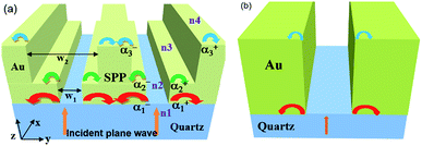
| | Fig. 1 (a) The schematic illustrates the parameters for the nanoledge structure and SPP generation by a plane wave at normal incidence. The w1 and w2 represent the slit widths at the Au–quartz and Au–air interfaces, and the α1+, α1−, α2+, α2−, α3+, α3− represent the SPP generation coefficients at the three interfaces (red, green, and blue arrows, respectively) with inverse propagation directions. The refractive indexes inside the slits are represented by n2 and n3, and those at the outer slits are presented by n1 and n4, when exposed in air, n2 = n3 = n4 = 1 (air), and n1 = 1.45 (quartz). (b) The schematic of a straight single nanoslit structure is shown as a comparison. | |
Results and discussion
Analytical considerations
In order to study nanoledge geometries that are of interest in practice and consider the geometric diffraction with the bounded SPP modes launching on the flat interfaces surrounding the slits, a mechanistic description for SPP generation is needed, especially the SPP scattering coefficients and efficiencies at the slit apertures. Fig. 1 illustrates schematic of a nanoledge structure in subwavelength thick gold film at quartz substrate (Fig. 1a) and a straight nanoslit structure (Fig. 1b) as a comparison. In this study, we focus on the SPP generation at the Au/medium interfaces upon light excitation without considering the height conditions (i.e. subwavelength thickness of the metallic film). Note that the thickness (height) predominately affects the SPP fundamental modes in the slit traveling upward and downward, not the SPP generation confined at the flat interfaces;29 hence it is not considered in detail here.
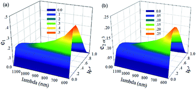
With the semi-analytical model (see Method section), the SPP excitation efficiency e for one side of the aperture is readily calculated with analytical techniques.30 Fig. 2 shows the decomposed SPP excitation efficiency e on one side of the aperture for the interfaces of the nanoledge as a function of the scaled slit width w′ and the incident light wavelength, from the visible to near-infrared (600–1200 nm). The SPP excitation is efficient at visible frequencies while e rapidly decreases with the increase of wavelength. For the interfaces surrounding the ledge structure, all of the optimal scaled slit widths are similar with a value of w′ = 0.2.
 |
| | Fig. 2 The SPP generation efficiencies e at the Au–quartz and Au–air interfaces are plotted as a function of λ and w′ obtained by the semi-analytical model. (a) Au–quartz interface e1 = |α1+(w1/2)|2 = |α1−(w1/2)|2; (b) Au–air interface, e2 = |α2+(w1/2)|2 = |α2−(w1/2)|2, the e3 has the same performance as e2 (see more in Fig. S1†). | |
If one selects n1 = 1.45 for quartz and n2 = n3 = n4 = 1 for air in the model,31 then the optimal nanoledge widths (Fig. 1a) are w1 = 0.14λ for the bottom Au–quartz slit and w2 = 0.2λ for the top Au–air slit. Moreover, at a visible wavelength of 600 nm, the SPP excitation efficiencies are fairly large. The maximum e is calculated as 0.496 for the Au–quartz interface and 0.224 for the Au–air interface of the nanoledge structure in Fig. 1. It is expected that the total SPP excitation efficiency e will result from a “superposition” of the SPP arising from all the interfaces of the nanoledge structures.
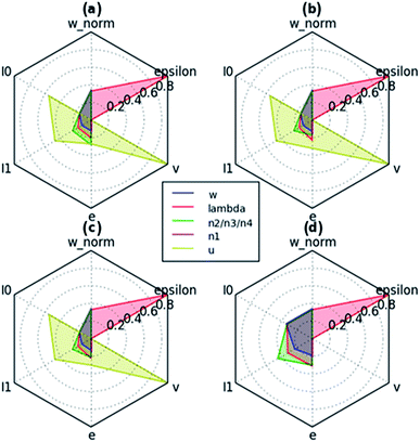
A factor analysis32 of the semi-analytical equations was performed in order to assess the correlations of w, λ, n1, n2/n3/n4 (n2 = n3 = n4 in this analysis), and u on the calculation variables of w′, I0, I1, e, v, and ε in the SPP analysis (see details in ESI, Fig. S2 and ESI†). Fig. 3 shows some radar plots of the influence factor coefficient for different cases. For the Au/quartz interface (Fig. 3a), the factor coefficient of the slit width w on the SPP generation efficiency, e, is 0.12, which is almost the same with that in the Au–air interfaces as shown in Fig. 3b. Moreover, the factor coefficient of the wavelength λ on e becomes larger from the Au–quartz interface to the Au-medium interfaces, in agreement with eqn (6), (11), and (15) (see Method section). Meanwhile, the factor coefficient of the refractive indices, n2/n3/n4 on e becomes larger while that of substrate n1 on e becomes smaller; evident from eqn (4), (9) and (13). Beside this, the factor coefficient of wavelength λ on dielectric constant ε or numerical factor u on v is 1 because of their one–one correspondence. Using Fig. 3a and b, we derived the total factor coefficient of each independent variable (w, λ, n1, n2/n3/n4, or u) on individual dependent variables (w′, I0, I1, e, v, or ε) and this is shown in Fig. 3c. In Fig. 3c one can see that the numerical factor u plays the most important part in calculating e, as a factor coefficient of 0.29 according to the yellow area shown. Note that the area is formed by the connection between the six spots (like the six factor coefficients of u on w′, I0, I1, e, v and ε). In order to more clearly understand the role of the slit width, w, in the analytical part (without u), the influence factor coefficient of w on e was obtained and found to be 0.17; see Fig. 3d. From this analysis and the physical considerations described above, the nanoledge widths, w1 and w2, play an important role in SPP generation.
 |
| | Fig. 3 Radar charts of the factor coefficients of factors (w, λ, n2/n3/n4, n1, u) on the calculation variables (w′, I0, I1, e, v, ε) in the semi-analytical model are shown for four scenarios. (a) the algebraic operation for e1 of SPP (red in Fig. 1) at the Au/quartz interface; (b) the algebraic operation for e2 or 3 of SPP (green and blue in Fig. 1a) at the Au/Air interfaces; (c) the factor analysis combining (a) with (b); and (d) the analytical part (without u and v) of scenario (c). | |
Numerical simulation
In order to study the optical transmission properties of the nanoledge structure with different w1 and w2, FDTD calculations were used to simulate the interaction between the metal and the incident light wave.
Fig. 4 summarizes some results of these simulations. Panel (a) in Fig. 4 shows the calculated typical transmission spectra for one selected nanoledge of w2 − w1 with 280–50 nm (geometries with w2 − w1 of 280–40 nm, 300–40 nm, and 300–50 nm also performed, see Fig. S8†). The four nanoledges were predicted to have high optical transmission (see Fig. 4b and Table S5†) because of the transmission resonance corresponding to the Au/quartz mode. The four nanoledge devices have a predicted maximum transmittance of about 27%. The insert in Fig. 4a shows the corresponding TE distribution (more details for the w2 − w1 of 280–50 nm nanoledge device are shown in Fig. S3a†). The SPP generation occurs at three different interfaces which are marked by the white arrows. This was further confirmed by the corresponding TM distributions, given in Fig. S3b.† Along with the resulting TM profiles at the reflected surface and at the transmitted surface (see Fig. S4†), it suggests that the transmission resonances may arise from localized surface plasmons along the x-direction and SPP propagating along the y-direction.33
 |
| | Fig. 4 Panel (a) shows the calculated typical transmission spectra of the w2 − w1 of 280–50 nm nanoledge system with the inserted corresponding TE field dynamics at 3 seconds calculated for the systems. Panel (b) shows the maximum transmission regarding different w1 and w2 in the nanoledge systems with a 3D inset view. Panel (c) shows the peak wavelength of 280–50 nanoslit system vs. refractive indices of bulk solutions, nmethanol ≈ 1.32, nwater ≈ 1.33, nacetone ≈ 1.35, nethanol ≈ 1.36, and nIPA ≈ 1.37 with a peak wavelength shift inset view. | |
The electromagnetic field distributions reveal that the plasmonic excitations arise from the Au/quartz interface and the gold/medium interfaces with the strength of Au/quartz > Au/air, which is consistent with the results of the semi-analytical model for SPP efficiencies of e1 > e2 > e3 for the four nanoledge devices. According to the analytical considerations, the optimal slit widths are w1 = 0.14λ and w2 = 0.2λ for maximum SPP generation. From the FDTD simulations results for w1 of 40/50 nm and w2 of 280/300 nm over a broad spectrum ranging from the visible to near-infrared, the w2 − w1 of 280 nm–50 nm nanoledge system is optimal; i.e., close to optimal slit widths and with the highest optical transmission (Fig. 4b). If we assume an incident light with wavelength of 600 nm, we obtain the scaled widths w′1 = 0.121, w′2 = 0.083 and w′3 = 0.467, corresponding to the three Au/medium interfaces from bottom to top, and the SPP generation efficiencies of e1 = 0.48, e2 = 0.18, and e3 = 0.16, which is consistent with the order of the TE field intensities of the three Au–medium interfaces; see the white arrows shown in Fig. 4a insert. These results indicate that the semi-analytical approach provides insight into the SPP generation efficiencies by enabling a decomposition analysis of the SP in such a complex perforated metal film nanostructure.
Fig. 4c shows an analysis in which the FDTD simulations are used to calculate the refractive index sensitivity of the optimal w2 − w1 of 280–50 nm nanoledge device. In these simulations the peak wavelength shift was monitored for different refractive indices of the external medium and chosen to mimic the index of refraction of common solvents; namely, methanol, deionized water, acetone, ethanol, and isopropyl alcohol (IPA).34 The calculated wavelength red shifted as the RI of the solvent increased, and the sensitivity was found to be 556 nm per RIU. Furthermore, the plot shows that the dependence of the peak wavelength on the bulk RI of the medium is linear, which makes the nanoledge system highly suitable for biosensing applications.
A comparison of semi-analytical approach and numerical simulation
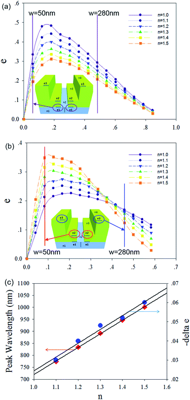
As a comparison between the FDTD and the semi-analytical decomposition analysis of SPP generation, Fig. 5 presents the main results of the predicted SPP-generation efficiencies e as a function of the nanoledge widths (w1, w2) and RIs (n2 = n3 = n4 = n) at the incident wavelength λ = 600 nm. For the bottom Au/quartz interface, the SPP generation efficiencies e (obtained from eqn (4) with w′1 = n1w1/λ) decrease as the surrounding medium's RI increases (up to 1.5) for the slit width w1 smaller than λ (Fig. 5a). In contrast, the SPP-generation efficiency e (e2/e3) of the Au/medium interfaces increase as the medium's RI increases for slit width below 0.33λ (∼200 nm at 600 nm incident light), and thereafter transitions to the same dependence as for the Au/quartz interfaces (Fig. 5b). With a specific nanoledge geometry of w1 = 50 nm and w2 = 280 nm, it is interesting to note that the total SPP generation efficiency change, −Δ(e1 + e2 + e3), has the same dependence on the bulk media RI as the EOT peak shift (Fig. 5c). Given that a weakened SPP generation efficiency correlates with a red shift of the optical transmission peak from a coupling of RI and geometry parameters (w′), the SP decomposition analysis suggests that, for the specific nanoledge w2 − w1 of 280–50 nm, the SPP generation efficiency (e2) of Au/medium interface in the center of the nanoledge would result in a blue shift as the RI increases, while a decrease of SPP generation efficiencies (e1, e3) at the bottom and top Au/medium interfaces would result in a red shift for the optical transmission. Indeed, the blue shift of optical transmission in a nanoslit cavity has been reported in a previous study.35
 |
| | Fig. 5 Decomposition of the SPP generation efficiency e is shown as a function of the nanoledge geometries at different refractive index of n2 = n3 = n4 (=n). Panel (a) shows the SPP generation efficiency e at the Au/quartz interfaces; the two vertical lines indicate the efficiency e at 50 nm and 280 nm slit width. Panel (b) shows the SPP generation efficiency e at the Au/RI-media interfaces, the red and blue lines illustrating the efficiency e of the slit width at 50 nm and 280 nm. Panel (c) compares the EOT peak shift and the total SPP generation efficiency changes as a function of bulk media RIs (see Table S6† and Fig. S5† for individual e values). | |
Experimental studies
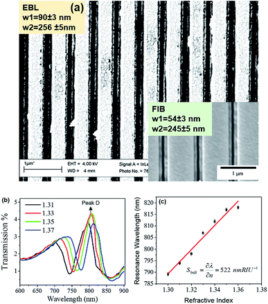
To further validate our analysis, electron beam lithography (EBL) and focused ion beam (FIB) milling were used to fabricate Au nanoledge structures in arrays (30 × 30 μm2), and the optical transmission spectra were measured as function of the change of refractive index in the nanoledge area. Fig. 6a inserted and Fig. 7a present AFM and SEM images of geometrically different nanoledge structures that were fabricated.
 |
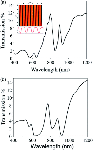
| | Fig. 6 Experimentally obtained transmission spectrum of a 600 nm periodicity nanoledge structure in air is illustrated in panel (a). The insert in (a) is the AFM image of the nanoledge structure with a cross along the white line is depicted; the scale bar is 1 micron. In panel (b) a FDTD calculated transmission spectrum is shown, in which the slit dimensions/geometry obtained from AFM. | |
 |
| | Fig. 7 (a) SEM images of two nanoledge fabricated by EBL and FIB, respectively; (b) the transmission spectra of the FIB fabricated nanoledge arrays (w2 − w1 = 245–54 nm) with changes of bulk refractive index; and (c) the primary peak position (peak D) as a function of refractive index obtained from (b). | |
The experimental transmission spectrum for a FIB fabricated nanoledge array collected in air with a periodicity of 600 nm is shown in Fig. 6a. It can be noted that FDTD calculations predict a sharper main transmission feature (Fig. 4a) in the transmission spectrum as compared to what is experimentally achieved. Broadening of the peaks in the experimental transmission spectrum may arise from fabrication imperfections. It should also be noted that the spectrophotometer, which has a wavelength resolution of 0.782 nm, will not be able to capture these sharp features into the experimental transmission spectrum. To account for fabrication defects, FDTD simulations were performed with realistic slit dimensions taken from AFM imaging of the focused ion beam fabricated nanoledge (Fig. 6a insert). The calculated transmission spectra of the 600 nm periodicity nanoledge structure is illustrated in Fig. 6b. With these dimensions, the main transmission peak appear less sharp and have much reduced intensity compared the idealized structure. This observation could account for differences in coupling of the cavity modes with SPP modes in the two geometries.
Fig. 7b–c shows the representative transmission spectra of the FIB fabricated nanoledge device (gold thin film on quartz) and the primary transmission peak (D) as a function of the medium RI in the nanoledge. As for the geometry w2 − w1 of 245–54 nm, the RI sensitivity (Sbulk) is 522 nm per RIU, while for the geometry 256 nm/90 nm, the RI sensitivity is 311 nm per RIU (see ESI Fig. S9†), which demonstrates a good quantitative agreement with the FDTD simulation. The RI sensitivity is somewhat less than the optimal SPP generation efficiency geometry with w2 − w1 of 280–50 nm obtained from the perfectly-conducting metal approximation.
Methods
Semi-analytical approach
Based on the mode orthogonality condition,23,36 the SPP generation efficiency is governed by the following equations:| |
 | (1) |
and| |
 | (2) |
where H and E represent the magnetic and electric field amplitudes, respectively, w is the width of the slit, and α+(w/2) and α−(w/2) represent SPP excitation coefficients at the exit sides of the slit.23 The strength of the SPP generation is provided by |α|2. Using this approach one can derive the following equation for the surface plasmon generation by a single straight slit mode:36,37| |
 | (3) |
with the assumption that the metal is a perfect conductor. This assumption simplifies the dependence of the geometric diffraction on the dielectric properties of the metal, and the dependence of the bounded SPP mode on the dielectric properties of the metal–dielectric interface.38 In eqn (3), λ is the wavelength of the incident light, ε is the dielectric constant, and n1 and n2 represent two refractive indexes of the two media on either side of the interface (see Fig. 1a).
Combining the SPP fundamental mode with transmission mode in the plane wave basis, we can obtain the SPP generation efficiencies on both sides of the aperture, under the assumption of α+(−w/2) = α−(w/2) = 0, regarding the electromagnetic field below and inside the slit. By generalizing the procedure used by Lalanne for a single straight slit (Fig. 1b),37,39,40 one can obtain the SPP generation efficiencies e at both sides of the apertures on the three Au interfaces; see Fig. 1a. For the Au/quartz interface e (red) is given by:
| |
 | (4) |
in which
| |
 | (5) |
| |
 | (6) |
where
w′ represents the scaled width and
u and
v are applied for numerical integration with
u2 +
v2 = 1.
For the slit mode case, the corresponding SPP efficiencies can be obtained by the following equation:37
| |
 | (8) |
with the assumption that the forward and backward fundamental modes compose the field in the slit and the normalization constants
N0 and
Np are given by
N0 =
w/(2
εn2) and
Np =
w/(2
εn1). For the inside Au/medium interface of the ledge (green),
e is expressed as:
| |
 | (9) |
with
| |
 | (10) |
| |
 | (11) |
Similarly, for the Au/medium interface at the top of the nanoledge aperture (blue), e is given by
| |
 | (13) |
with
| |
 | (14) |
| |
 | (15) |
Details of the derivation of these results are provided in the ESI.† Because the full integrand, weighted by v, is singular over the interval of −1 and +1 and complex for |u| > 1, the integrals I0(I′0, I′′0), and I1(I′1, I′′1), were calculated numerically.37,41 Tables S1–S4† provide numerical results for different values of the normalized slit width w′ and wavelength λ with the corresponding dielectric constant values of quartz.
Numerical simulation
The metal's dielectric response was modeled by a Drude–Lorentz model,42| |
 | (17) |
where ε is the permittivity, ω0n is the resonant frequency, Γn is the damping coefficient, and x0 is the permittivity at ω0. By using a single resonance and the Fourier transform of the polarization in the algorithm, the FDTD formalism was used to calculate the transverse electric (TE) and transverse magnetic (TM) fields.28
The geometry of the nanoledge structure was modeled in three-dimensional (3D) environments. The dielectric function of Au used in the simulations was from Johnson and Christy43 and the substrate was simulated as an infinite block with a dielectric constant of silicon dioxide taken from Palik.44 The simulations were performed using a single aperture as the unit cell with periodic boundary conditions in the y-direction to describe an infinite rectangular array and perfectly matched layers in the boundary along the x and z-direction. The period of the nanoslit array is 600 nm and the heights of the two slits are 50 nm and 150 nm, respectively. Note that the period and height are chosen to correspond to our previous work with nanoplasmonic nanofluidics.45 As with the experiments, the calculations consider a linearly polarized broadband plane wave source, which propagates through the quartz substrate and is incident on the back surface of the gold layer at normal incidence.
Device fabrication and testing
Subwavelength nanoledge structures were fabricated using electron beam lithography (EBL) and focused ion beam (FIB) techniques. Sample imaging was done using an SEM in the nanofabrication systems. Spectral characterization of the nanoledge arrays was carried out using a microspectrophotometer (Craic QDI 2010).46 The details of the experimental procedures and supporting data are included in the ESI.†
Conclusions
In conclusion, we extended a semi-analytical model to perform a decomposition analysis of the SPP wave generation at metallic interfaces perforated by a subwavelength gold nanoledge structure. The factor analysis of parameters (geometric, dielectric-RI, and incident wavelength) relevant to surface plasmon (SP) generation has been quantitatively investigated for the prediction of surface plasmon polariton (SPP) generation efficiency. The rigorous formalism for the model has been validated by comparisons with the FDTD modelling of the EOT and its sensitivity of RI changes and by experimental testing of fabricated nanoledge devices through measurement of their optical transmission and RI sensitivity. The analysis shows that SPP-generation is very efficient for the gold film nanoledge device. The reported semi-analytical approach provides a new tool for a quantitative decomposition analysis of SPP generation in other related slit structures and should prove useful for plasmonic device development.
Acknowledgements
J. W. and Z. Z. acknowledge the financial support from US NSF (Grant # 1511194). J. W. and Z. Z. also kindly acknowledge the support from JSNN. DHW and MM acknowledge financial support from NIH Grant # 1R21RR026221-01.
Notes and references
- S. Lal, S. Link and N. J. Halas, Nat. Photonics, 2007, 1, 641–648 CrossRef CAS.
- J. Li, C. Chen, L. Lagae and P. Van Dorpe, J. Phys. Chem. C, 2015, 119, 29116–29122 CAS.
- R. Quidant and M. Kreuzer, Nat. Nanotechnol., 2010, 5, 762–763 CrossRef CAS PubMed.
- M. I. Stockman, Opt. Express, 2011, 19, 22029–22106 CrossRef PubMed.
- M. A. Beuwer, M. W. J. Prins and P. Zijlstra, Nano Lett., 2015, 15, 3507–3511 CrossRef CAS PubMed.
- A. A. Al Balushi and R. Gordon, ACS Photonics, 2014, 1, 389–393 CrossRef CAS.
- A. G. Brolo, Nat. Photonics, 2012, 6, 709–713 CrossRef CAS.
- M. E. Stewart, C. R. Anderton, L. B. Thompson, J. Maria, S. K. Gray, J. A. Rogers and R. G. Nuzzo, Chem. Rev., 2008, 108, 494–521 CrossRef CAS PubMed.
- O. Tokel, F. Inci and U. Demirci, Chem. Rev., 2014, 114, 5728–5752 CrossRef CAS PubMed.
- M. Couture, L. S. Live, A. Dhawan and J.-F. Masson, Analyst, 2012, 137, 4162–4170 RSC.
- E. Hendry, R. V. Mikhaylovskiy, L. D. Barron, M. Kadodwala and T. J. Davis, Nano Lett., 2012, 12, 3640–3644 CrossRef CAS PubMed.
- K.-L. Lee, P.-W. Chen, S.-H. Wu, J.-B. Huang, S.-Y. Yang and P.-K. Wei, ACS Nano, 2012, 6, 2931–2939 CrossRef CAS PubMed.
- T. W. Ebbesen, H. J. Lezec, H. F. Ghaemi, T. Thio and P. A. Wolff, Nature, 1998, 391, 667–669 CrossRef CAS.
- A. A. Yanik, M. Huang, O. Kamohara, A. Artar, T. W. Geisbert, J. H. Connor and H. Altug, Nano Lett., 2010, 10, 4962–4969 CrossRef CAS PubMed.
- T. G. Mayerhöfer, R. Knipper, U. Hübner, D. Cialla-May, K. Weber, H.-G. Meyer and J. Popp, ACS Photonics, 2015, 2, 1567–1575 CrossRef.
- O. Hess, J. B. Pendry, S. A. Maier, R. F. Oulton, J. M. Hamm and K. L. Tsakmakidis, Nat. Mater., 2012, 11, 573–584 CrossRef CAS PubMed.
- L. Feuz, P. Jönsson, M. P. Jonsson and F. Höök, ACS Nano, 2010, 4, 2167–2177 CrossRef CAS PubMed.
- S. S. Aćimović, M. A. Ortega, V. Sanz, J. Berthelot, J. L. Garcia-Cordero, J. Renger, S. J. Maerkl, M. P. Kreuzer and R. Quidant, Nano Lett., 2014, 14, 2636–2641 CrossRef PubMed.
- S.-H. Chang, S. Gray and G. Schatz, Opt. Express, 2005, 13, 3150–3165 CrossRef PubMed.
- P. Lalanne and J. P. Hugonin, Nat. Phys., 2006, 2, 551–556 CrossRef CAS.
- A. E. Schlather, N. Large, A. S. Urban, P. Nordlander and N. J. Halas, Nano Lett., 2013, 13, 3281–3286 CrossRef CAS PubMed.
- F. J. Garcia-Vidal, L. Martin-Moreno, T. W. Ebbesen and L. Kuipers, Rev. Mod. Phys., 2010, 82, 729–787 CrossRef.
- P. Lalanne, J. P. Hugonin, H. T. Liu and B. Wang, Surf. Sci. Rep., 2009, 64, 453–469 CrossRef CAS.
- H. Liu and P. Lalanne, Nature, 2008, 452, 728–731 CrossRef CAS PubMed.
- J. P. Litz, J. P. Camden and D. J. Masiello, J. Phys. Chem. Lett., 2011, 2, 1695–1700 CrossRef CAS.
- T. Tanemura, K. C. Balram, D.-S. Ly-Gagnon, P. Wahl, J. S. White, M. L. Brongersma and D. A. B. Miller, Nano Lett., 2011, 11, 2693–2698 CrossRef CAS PubMed.
- D. M. Solís, J. M. Taboada, F. Obelleiro, L. M. Liz-Marzán and F. J. García de Abajo, ACS Nano, 2014, 8, 7559–7570 CrossRef PubMed.
- Z. Zeng, Y. Liu and J. Wei, TrAC, Trends Anal. Chem., 2016, 75, 162–173 CrossRef CAS.
- L. Aigouy, P. Lalanne, J. P. Hugonin, G. Julié, V. Mathet and M. Mortier, Phys. Rev. Lett., 2007, 98, 153902 CrossRef CAS PubMed.
- E. Skudrzyk, The Foundations of Acoustics: Basic Mathematics and Basic Acoustics, Springer-Verlag Wien, 1971 Search PubMed.
- Handbook of Optical Constants of Solids, Academic Press, Burlington, 1997 Search PubMed.
- P. Kline, An easy guide to factor analysis, Taylor and Francis, Hoboken, NJ, 2014 Search PubMed.
- A. E. Cetin, D. Etezadi, B. C. Galarreta, M. P. Busson, Y. Eksioglu and H. Altug, ACS Photonics, 2015, 2, 1167–1174 CrossRef CAS.
- M. Sanders, Y. Lin, J. Wei, T. Bono and R. G. Lindquist, Biosens. Bioelectron., 2014, 61, 95–101 CrossRef CAS PubMed.
- Y. S. Jung, J. Wuenschell, H. K. Kim, P. Kaur and D. H. Waldeck, Opt. Express, 2009, 17, 16081–16091 CrossRef CAS PubMed.
- P. Lalanne, J. P. Hugonin and J. C. Rodier, Phys. Rev. Lett., 2005, 95, 263902 CrossRef CAS PubMed.
- P. Lalanne, J. P. Hugonin and J. C. Rodier, J. Opt. Soc. Am. A, 2006, 23, 1608–1615 CrossRef CAS PubMed.
- W. Yao, S. Liu, H. Liao, Z. Li, C. Sun, J. Chen and Q. Gong, Nano Lett., 2015, 15, 3115–3121 CrossRef CAS PubMed.
- P.-K. Wei, H.-L. Chou, Y.-R. Cheng, C.-H. Wei, W. Fann and J. O. Tegenfeldt, Opt. Commun., 2005, 253, 198–204 CrossRef CAS.
- Y. Xie, A. Zakharian, J. Moloney and M. Mansuripur, Opt. Express, 2004, 12, 6106–6121 CrossRef PubMed.
- P. Chimento, PHD Doctoral, Leiden University, 2013.
- A. Vial, A.-S. Grimault, D. Macías, D. Barchiesi and M. L. de la Chapelle, Phys. Rev. B: Condens. Matter Mater. Phys., 2005, 71, 085416 CrossRef.
- P. B. Johnson and R. W. Christy, Phys. Rev. B: Condens. Matter Mater. Phys., 1972, 6, 4370–4379 CrossRef CAS.
- H. R. Philipp, in Handbook of Optical Constants of Solids, ed. E. D. Palik, Academic Press, Burlington, 1997, pp. 749–763, DOI:10.1016/B978-012544415-6.50038-8.
- J. Wei, H. Song, S. Singhal, M. Kofke, M. Mendis and D. H. Waldeck, ASME Proceedings | Micro/Nanofluidics and Lab-on-a-Chip, Atlanta, GA, 2012 Search PubMed.
- M. N. Mendis, H. S. Mandal and D. H. Waldeck, J. Phys. Chem. C, 2013, 117, 25693–25703 CAS.
Footnote |
| † Electronic supplementary information (ESI) available: Additional mathematical derivation, programming and data analysis, experimental description, supporting figures and tables. See DOI: 10.1039/c6ra01105e |
|
| This journal is © The Royal Society of Chemistry 2016 |
Click here to see how this site uses Cookies. View our privacy policy here. 