Morphology-controlled synthesis of NiO films: the role of the precursor and the effect of the substrate nature on the films' structural/optical properties
Sergio Battiatoa,
Maria M. Giangregoriob,
Maria R. Catalanoa,
Raffaella Lo Nigroc,
Maria Losurdo*b and
Graziella Malandrino*a
aDipartimento di Scienze Chimiche, Università degli Studi di Catania, INSTM UdR-Catania, Catania, 95125, Italy. E-mail: gmalandrino@unict.it
bCNR-NANOTEC, Istituto di Nanotecnologia, Dipartimento di Chimica, Università di Bari, via Orabona 4, 70126 Bari, Italy. E-mail: maria.losurdo@cnr.it
cIstituto per la Microelettronica e Microsistemi IMM-CNR, Strada VIII n. 5, 95121 Catania, Italy
First published on 10th March 2016
Abstract
NiO thin films were grown through metalorganic chemical vapour deposition (MOCVD) on quartz and LaAlO3 (001) single crystal substrates. Two different volatile and thermally stable nickel β-diketonate adducts, Ni(hfa)2·tmeda and Ni(tta)2·tmeda [H-hfa = 1,1,1,5,5,5-hexafluoro-2,4-pentandione; tmeda = N,N,N′,N′-tetramethylethylendiamine, Htta = 2-thenoyltrifluoroacetone], were applied as precursors for NiO film growth. The comprehensive study, applying two different precursors and changing the processing parameters, allowed for morphological control of the deposited NiO films. The AFM analyses indicated different values of roughness for NiO films obtained from the two different precursors and those from Ni(tta)2·tmeda showed a lower roughness. In addition, UV-Vis and ellipsometric measurements on NiO films grown from the Ni(tta)2·tmeda show higher transparency, fewer defects/impurities, better crystallinity and a higher refractive index than films deposited using the Ni(hfa)2·tmeda source. Raman spectroscopy confirmed the antiferromagnetic nature of the NiO layers. Work functions, around 5.1 eV, were measured by Kelvin Probe Force Microscopy for NiO films grown from Ni(tta)2·tmeda. The relationship between the precursor/substrate nature and film properties allowed us to define the best precursor and conditions for the MOCVD growth of good quality NiO films.
Introduction
Nickel oxide (NiO) is among the most widely investigated transition metal oxides (TMOs), and it actually represents a model compound for TMOs with the sodium chloride structure.1 It exhibits only a very small deviation from the ideal stoichiometry in contrast to cobalt oxide (CoO) and especially the wüstite iron oxide (FeO) phase.NiO has also drawn much attention due to its utilization for several applications such as gas sensors,2,3 catalysts4,5 and electrochromic devices.6–9 Other applications include its use as transparent conducting oxide (TCO) films. TCO films such as indium oxide, tin oxide and zinc oxide are of practical use as transparent electrodes and window coatings, but they are all n-type semiconductors. A desirable hole injecting contact would be based on injection into the valence band of a p-type semiconducting oxide. NiO is a potential p-type TCO candidate. NiO is known to become a p-type semiconductor when monovalent atoms such as Li+,10,11 are used as a dopant or when NiO composition deviates from stoichiometry, whereas stoichiometric NiO is an insulator with high resistivity (ρ > 1013 Ω cm) at room temperature. Due to their electric properties, p-type semiconducting NiO films have been used as efficient-enhancing anode interfacial layers in polymer bulk-heterojunctions,12–14 and dye-sensitized solar cells10,15–18 and as hole transporting19 or as electron blocking20 layers in light-emitting devices. Furthermore, thin films of NiO, due to their antiferromagnetic properties with a Néel point (TN) of 523 K are very useful as the antiferromagnetic layer of spin-valve superlattice films. Pure NiO exhibits antiferromagnetic ordering with planes of opposite spins being repeated in alternating order along the [111] direction. Below the Néel temperature, the magnetic ordering in NiO is accompanied by a slight rhombohedral distortion (at 20 °C, a = 2.9518 Å, α = 60.42°).21 Magnon excitations in pure NiO nanoparticles and single crystals have been successfully studied by Raman spectroscopy.22–24 The strong magnetic Raman response is caused by the Ni–O superexchange mechanism. Clearly, a trade-off exists among the magnetic, electrical and optical properties of NiO films, which correlates with the microstructure and deposition methodologies.
To date, NiO films and nanostructures have been prepared by various deposition processes such as sputtering,25 chemical spray pyrolysis,26 sol–gel,27 sparking methods,28 solvothermal synthesis,29 aerosol-assisted chemical vapour deposition (AACVD),30,31 photo-assisted chemical vapour deposition,32 metalorganic chemical vapor deposition (MOCVD)33–35 and atomic layer deposition (ALD).36,37
The CVD processes have the potential advantage of being very reliable and reproducible methods for the fast production of films with a high uniformity degree in both thickness and composition over large areas. In particular, various precursors have been tested such as bis-cyclopentadienyl nickel,33,38 bis-(ethylcyclopentadienyl) nickel,39 nickel bis(1-dimethylamino-2-methyl-2-butanolate),34 and nickel(II) acetylacetonate.31
Here, we report on a comprehensive study for the MOCVD deposition of polycrystalline NiO films relating the use of two different precursors and different substrates on the structural, morphological and functional properties of the deposited layers. Two different nickel sources were synthesized and applied: Ni(tta)2·tmeda and Ni(hfa)2·tmeda [H-hfa = 1,1,1,5,5,5-hexafluoro-2,4-pentandione; tmeda = N,N,N′,N′-tetramethylethylendiamine, Htta = 2-thenoyl-trifluoroacetone]. A correlation between the nature of the nickel β-diketonate precursors and the properties of the NiO films is addressed. In regard to substrates, quartz and LaAlO3 (001) single crystal substrates, hereafter indicated as LAO, have been chosen in view of specific applications. In particular, quartz has been used to test the optical properties, while the LAO substrate is interesting to test the antiferromagnetic properties, since a very important issue in the magnetic thin film fabrication is to find a substrate with a good lattice match vs. the growing film.
Structural information and the lattice parameters of thin films were determined through X-ray diffraction (XRD) measurements, while film morphological characteristics were investigated using field emission scanning electron microscopy (FE-SEM) and atomic force microscopy (AFM). The work function of NiO films was measured through Kelvin probe electrical force microscopy (KPEFM), and Hall measurements of the carriers mobility were analysed using the van der Pauw configuration.
The optical properties have been investigated through UV-Vis and ellipsometric measurements, while the antiferromagnetic characteristics have been tested using Raman spectroscopy.
Experimental
Precursor synthesis
The synthesis and characterization of Ni(tta)2·tmeda40 were reported elsewhere. For the synthesis of the present Ni(hfa)2·tmeda, a new strategy was adopted, whose synthesis had been previously reported.41 The volatile and thermally stable Ni(hfa)2·tmeda complex was prepared by the reaction of Ni(CH3COO)2·4H2O (1.932 g, 7.763 mmol) suspended in dichloromethane (50 ml) with tmeda (0.821 g, 7.065 mmol) and H-hfa (2.940 g, 14.130 mmol). The mixture was refluxed with stirring for 1 h. The solution was collected by filtration under vacuum and the excess Ni(CH3COO)2·4H2O was filtered off. Green-emerald crystals were obtained upon solvent evaporation that were washed two times in pentane and recovered by filtration. The reaction yield was 88%. The melting point of the crude product was 103–107 °C/760 Torr.Thermal measurements were made using a Mettler Toledo TGA/SDTA 851e, a TC 10 processor and a DSC 30 calorimeter. Thermal investigations were carried out under purified nitrogen flow (30 sccm) at atmospheric pressure using a heating rate of 5 °C min−1. Weights of the samples were between 10 and 15 mg (TGA) and 4–10 mg (DSC). The temperature was measured with an accuracy of ±0.1 °C.
MOCVD of thin films
NiO films were prepared in a reduced-pressure, horizontal, hot-wall MOCVD reactor from the Ni(tta)2·tmeda and Ni(hfa)2·tmeda precursors contained in a resistively heated alumina boat. In this study, the precursor evaporation temperature was maintained at 170 °C for Ni(tta)2·tmeda and 90 °C for Ni(hfa)2·tmeda. Single crystals of LaAlO3 (001) and quartz (by Crystal GmbH, Berlin, Germany) were used as substrates. The carrier gas Ar was maintained at 150 standard cubic centimetres per min, sccm. In order to investigate the interplay between microstructure and functional properties, the following parameters were investigated, in addition to the different precursors and substrates: (i) the deposition temperature, varied in the 350–550 °C range; (ii) the flow of the reaction gas O2 (50, 200 or 600 sccm). The total pressure in the reactor was about 2–6 Torr. The mass flows were controlled with MKS 1160 flow meters using an MKS type 247 electronic control unit. Deposition time was fixed at 60 min, yielding films of thickness in the 170–250 nm range, depending on the deposition temperature and on the precursor nature.Film characterization
Film structure was analysed by X-ray diffraction (XRD) and Raman spectroscopy. XRD patterns were recorded on a Bruker-AXS D5005 θ–θ diffractometer, using a Göbel mirror parallel to the Cu Kα radiation operating at 40 kV and 30 mA. A 0.05° increment step was used for the XRD patterns reported in Fig. 3 and 0.02° for the patterns used for the a-axis determination (Fig. 4) and for the rocking curves. Graphite paste was painted on the NiO film surface to be used as a standard for the correct evaluation of the peak position. Pole figures were recorded on a θ–2θ Bruker-AXS D5005 diffractometer equipped with an Eulerian cradle.Raman spectra were acquired using a LabRAM HR Horiba-Jobin Yvon spectrometer with 473 nm excitation under ambient conditions at low laser power (<1 mW) to avoid laser-induced damage.
Film morphology was analyzed by field emission gun scanning electron microscopy (FE-SEM) and atomic force microscopy (AFM). FE-SEM images were taken on Au-coated samples using a ZEISS SUPRA 55 VP field emission microscope.
Measurements of non-contact intermittent mode atomic force microscopy (AFM) and Kelvin probe were performed using an AutoProbe CP Thermomicroscope to investigate morphology and work function, WF.42 NiO WF was determined using as reference the WF of a gold contact (WF = 4.75 eV)43 evaporated on top of the NiO. The Au contacts were also used to measure the conductivity and carrier mobility in the Van der Paw configuration (over an area of 1 cm2 between the four Au contacts) using a Hall-mobility system.
The film composition and purity were analysed by energy dispersive X-ray analysis (EDX) using an INCA-Oxford windowless detector. NiO films were free of contamination from elements present in the ligand such as F, S, or C. Very small peaks around 0.27 keV, due to the C Kα peak, were found in some films grown from the Ni(hfa)2·tmeda.
Optical characterization was performed by spectroscopic ellipsometry (SE) and optical absorption. Spectrophotometric measurements from 300 to 800 nm were taken at near-normal incidence on a double-beam Jasco V-650 spectrophotometer. SE measurements were carried out in the 0.75–6.5 eV range with a phase-modulated spectroscopic ellipsometer (UVISEL-Jobin Yvon) at a 70° angle of incidence to determine film thickness and optical properties, namely, the refractive index, n, the extinction coefficient, k, and optical bandgap. In particular, ellipsometry measures the ratio, ρ, of the Fresnel reflection coefficient of the p-polarized (parallel to the plane of incidence of the linearly polarized light beam) and s-polarized (perpendicular to the plane of incidence) light reflected from the surface through the ellipsometric angles Ψ and Δ defined by the following equation:
ρ = tan![[thin space (1/6-em)]](https://www.rsc.org/images/entities/char_2009.gif) Ψ Ψ![[thin space (1/6-em)]](https://www.rsc.org/images/entities/char_2009.gif) exp(iΔ), exp(iΔ), |
![[thin space (1/6-em)]](https://www.rsc.org/images/entities/char_2009.gif) Ψ = |Ep|/|Es| and Δ = δp − δs represent the amplitude and phase variation of the electric field vector associated with the light electromagnetic wave, respectively. ρ is related to the film dielectric function, ε = ε1 + iε2, and complex refractive index, N = (n + ik), through the following equation:
Ψ = |Ep|/|Es| and Δ = δp − δs represent the amplitude and phase variation of the electric field vector associated with the light electromagnetic wave, respectively. ρ is related to the film dielectric function, ε = ε1 + iε2, and complex refractive index, N = (n + ik), through the following equation:ε = ε1 + iε2 = N2 = (n + ik)2 = sin![[thin space (1/6-em)]](https://www.rsc.org/images/entities/char_2009.gif) 2ϕ[1 + tan2 2ϕ[1 + tan2![[thin space (1/6-em)]](https://www.rsc.org/images/entities/char_2009.gif) ϕ(1 − ρ)2/(1 + ρ)2], ϕ(1 − ρ)2/(1 + ρ)2], |
In order to estimate the optical properties of the NiO thin films from the ellipsometric measurements, a simple two-layer model, including the NiO bulk layer and the surface roughness layer, was used. The SE analysis showed that the various films had a different density that depended on the deposition conditions, and once the optical functions for the most dense NiO layer were found, all other films were modeled using an effective medium approximation44 of the NiO and voids, given as follows:
The complex dielectric functions, ε = ε1 + iε2 and refractive index, N = n + ik = √ε, of NiO were parameterized using a combination of Tauc–Lorentz oscillators.45,46
Results and discussion
Thermal properties of the precursors: Ni(hfa)2·tmeda and Ni(tta)2·tmeda
The Ni(β-diket)2·tmeda precursors were synthesized through a one pot reaction from nickel acetate, β-diketone and tmeda in dichloromethane. The presently used synthesis of the adduct Ni(hfa)2·tmeda showed some advantages with respect to the previously reported one.41 In fact, the previous synthesis required a more demanding procedure: the formation of the complex in water solution, the sequential extraction with 1,2-dichloroethane and re-crystallization with the same solvent. Our synthesis used a slight excess of the acetate, which allowed for a simple separation of unreacted reagents, yielding the green-emerald crystalline product in a high yield (88%).The thermal behavior of the present Ni(tta)2·tmeda and Ni(hfa)2·tmeda precursors was investigated by thermogravimetric (TG) analyses at atmospheric pressure in a purified nitrogen flow (Fig. 1).
 | ||
| Fig. 1 TG (upper panel) and DTG (lower panel) profiles of Ni(hfa)2·tmeda and Ni(tta)2·tmeda complexes under N2 flow at atmospheric pressure in the 30–400 °C temperature range. | ||
The thermogravimetric first derivative (DTG) of Ni(tta)2·tmeda consists of a single peak, thus indicating that the precursor evaporated quantitatively in the 200–330 °C range, with less than 2% residue left at 350 °C. A similar behaviour could be observed for the Ni(hfa)2·tmeda, whose evaporation occurs in the 120–200 °C temperature range, with about 2% residue at 350 °C. It can be concluded that both Ni(tta)2·tmeda and Ni(hfa)2·tmeda precursors show a clean vaporization with a low residue, as required for MOCVD applications.
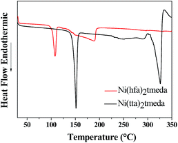
In Fig. 2, the differential scanning calorimetry (DSC) curves of Ni(tta)2·tmeda and Ni(hfa)2·tmeda are reported.
The DSC scans show evidence of endothermic peaks due to melting at 151.3 °C and 106.7 °C, respectively, for Ni(tta)2·tmeda and Ni(hfa)2·tmeda. Both precursors evaporated from melts in the 250–330 °C and 125–195 °C temperature ranges, respectively.
Impact of precursors and substrates on structural properties of NiO films
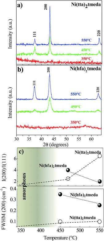
The structure of the films, as determined by XRD, is summarised for deposition on quartz substrates in Fig. 3.In particular, Fig. 3a and b show the XRD patterns of NiO films deposited on quartz substrates in the 350–550 °C temperature range with a 200 sccm oxygen flow from the Ni(tta)2·tmeda and Ni(hfa)2·tmeda precursors, respectively. For both precursors, 350 °C yielded amorphous NiO films, while at higher temperatures of 450 °C and 550 °C, the films were polycrystalline, as inferred by the presence of the 2θ peaks at 37.30°, 43.35° and 62.90° that correspond to the 111, 200 and 220 reflections. Note that only the reflection with hkl, all odd or all even, were observed due to the face-centered cubic lattice. In addition, the observed intensities did not match those typical of polycrystalline powder reported in the ICDD no. 47-1049. In particular, the I(200)/I(111) ratio and the full width at half maximum, FWHM, of the 200 peak (Fig. 3c), reported as a function of temperature and precursor type, indicated that the Ni(tta)2·tmeda yields NiO films with improved crystallinity and a slight preferential orientation along the 〈001〉 direction with the increase of deposition temperature.
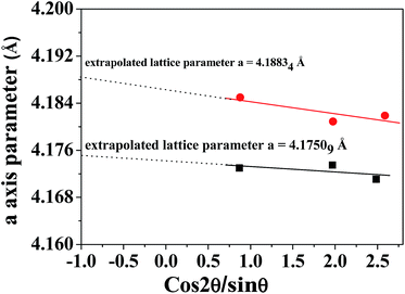
Therefore, considering that XRD data indicate 550 °C as the temperature condition to produce NiO films of better crystallinity, the unit cell parameter a has been extrapolated for films grown under these conditions from the two precursors following the diagram reported in Fig. 4.47
The extrapolated a-axis value is 4.1750 Å and 4.1883 Å for films grown from the Ni(tta)2·tmeda and the Ni(hfa)2·tmeda precursors, respectively. In particular, the a-axis of the films grown from Ni(tta)2·tmeda compares well with the 4.17710 Å theoretical value for the bulk NiO phase, indicating that these films are stoichiometric and of good quality.
Therefore, NiO films have been grown on a LAO (001) substrate under the optimized conditions obtained for depositions on quartz from the Ni(tta)2·tmeda.
The LAO substrate was chosen to have an appropriate lattice match, because if the lattices are well suited for one another, the surface of a thin film appears smooth and flawless. If the spacing between atoms in the substrate is too different from that of the overlying film, then the film may exhibit wrinkling, clumping, or other defects and these surface characteristics may affect the magnetic properties. The LAO substrate had a perovskite structure, whose unit cell can be described as pseudo-cubic with a lattice constant aps = 3.792 Å.
Fig. 5a presents the XRD diffraction pattern of the sample deposited on LAO (001) at 550 °C and exhibits only the NiO 002 and 004 reflections at 2ϑ = 43.30° and 95.35° in addition to the peaks at 2θ = 23.45°, 2θ = 48.15° and 2θ = 75.30° associated with the LAO 001, 002 and 003 reflections, respectively. Therefore, the NiO films grown on LAO (001) were purely 〈001〉 oriented. The grain dispersion was investigated by measuring the rocking curve of the 002 reflection at 43.30° (Fig. 5b). The full width at half maximum (FWHM) value of 0.94° indicated a good out-of-plane alignment of the NiO films. The in-plane alignment was studied by recording the (111) pole figure (2θ = 37.25°) of the NiO films (inset in Fig. 5a). The pole figure shows four poles observed at Ψ = 54° for every 90° degrees of ϕ, as expected for a cubic symmetry.
In addition, the in-plane relationship of NiO films relative to the underlying LAO substrate was obtained from Φ-scans of the NiO/LAO system (Fig. 5c). Φ-scans have been recorded using the NiO 111 reflection (2θ = 37.25°) and the LAO 111 reflection (2θ = 41.20°) as poles at a 54° Ψ tilt angle. The four peaks from the NiO (111) plane were coincident with the (111) LAO Φ positions. This clearly demonstrated that a cube-on-cube growth was observed for the NiO on LAO substrate, thus the [100] and [010] axis directions were aligned for the film and the substrate (i.e. NiO 〈100〉 ‖ LAO 〈100〉). These findings may be compared with the studies on heteroepitaxial growth of NiO on AlGaN.48–50 In that case, due to the hexagonal structure of the substrate, an epitaxial growth of the {111} NiO plane on the (0001) substrate plane occurred.
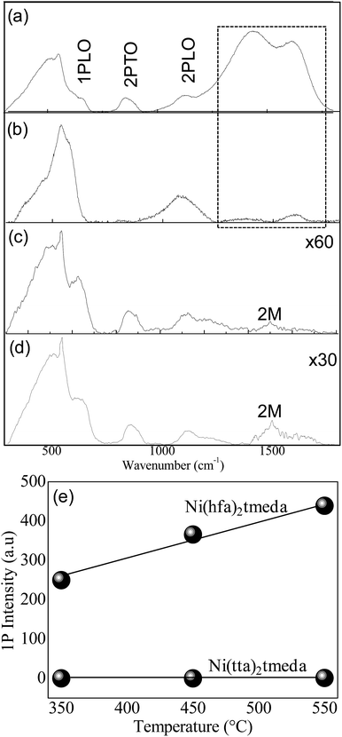
Additional microstructure information as well as the interplay between the microstructure and antiferromagnetic character of the films were obtained by Raman spectroscopy, since the NiO electronic structure, captured in its Raman spectrum, evolved with its stoichiometry, quality and antiferromagnetic properties.23 The vibrational bands corresponding to the one-phonon (1P) longitudinal optical (LO) mode (∼570 cm−1), the two-phonon (2P) 2TO (∼870 cm−1) and 2LO (∼1100 cm−1) modes and the band due to a two-magnon (2M) scattering at ∼1490 cm−1 are observed in Fig. 6.
A main difference observed between films from the two precursors is the presence of bands at 1350 cm−1 and 1600 cm−1 (Fig. 6a and b), indicating carbon contamination for NiO films deposited from Ni(hfa)2·tmeda, especially at 450 °C.
This may be related to the lower crystalline quality (Fig. 3) and gives indication that for this precursor, the transition from amorphous (350 °C) to polycrystalline (450 °C) is still negatively affected by the carbon-contaminations and that 550 °C is necessarily the minimal temperature to have acceptable polycrystallinity with larger crystallites (as can be also seen in Fig. 7) and reduced contaminations.
In contrast, carbon contamination was absent in the films from Ni(tta)2·tmeda at any deposition temperature. Furthermore, the 2M-scattering band around 1490 cm−1 indicates that films from Ni(tta)2·tmeda were in the antiferromagnetic phase.
The 1P broad band is a disorder-induced band that originates from Ni vacancies and its intensity has been related51 to the film quality. The intensity of the 1P band measured for films of comparable thickness under the same Raman acquisition conditions (measured also the same day) is plotted in Fig. 6e, indicating a lower density of Ni-vacancies for films from the Ni(tta)2·tmeda precursor. Thus, the poorer crystallinity detected by XRD can be associated with higher carbon-contaminations induced by the Ni(hfa)2·tmeda and could also be associated with a higher disorder due to Ni-vacancies. In contrast, the better crystallinity and stoichiometry are consistent with the lower intensity of 1P band and antiferromagnetic character inferred by Raman analysis of films from Ni(tta)2·tmeda.
Morphological properties of NiO films
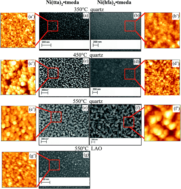
The NiO films have mirror-like surfaces and are also homogeneous in terms of morphology, over the whole area, as indicated by FE-SEM and AFM images, shown in Fig. 7 and 8. For both precursors, the grain size increased with increasing deposition temperature. The increased grain size with temperature was expected, since higher temperatures give rise to higher mobility of the atoms/molecules on the surface, thus favoring growth vs. nucleation and producing films with larger grains.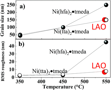 | ||
| Fig. 8 Evolution of the (a) grain size and (b) roughness (RMS) as a function of temperature, precursor and substrate. | ||
In particular, at the lowest temperature of 350 °C, films deposited from both precursors had very smooth surfaces and very small grains of about 50 nm (Fig. 7a and b), in accordance with the amorphous nature of the films. At higher temperature, films grown from the Ni(tta)2·tmeda showed homogeneous surfaces with grain dimensions going from about 100 nm at 450 °C (Fig. 7c) to 150 nm at 550 °C (Fig. 7e).
In the case of films deposited from the Ni(hfa)2·tmeda, a flat and homogeneous surface with small grains of 80 nm was observed at 450 °C (Fig. 7d), whereas large structured leaf-like 250–300 nm grains were found at 550 °C (Fig. 7f).
The film deposited at 550 °C on LAO (001) substrate (Fig. 7g) exhibited a smooth surface with crystalline cubic grains of about 70–80 nm. The dependence of grain size on temperature as well as the root mean square (RMS) roughness by AFM is reported in Fig. 8, supporting a smoother morphology for films from Ni(tta)2·tmeda on both quartz and LAO substrates with a RMS roughness going from 3 to 8 nm, whereas an increase of roughness with temperature from 2.5 nm to 45 nm was observed for films from Ni(hfa)2·tmeda.
Optical properties of NiO films
The optical properties have been tested through UV-Vis and ellipsometric measurements. The transmittance spectra show that the NiO films from Ni(tta)2·tmeda (Fig. 9a) were highly transparent in the visible region, with optical transmission generally decreased with increased deposition temperature, probably because of increased scattering due to the larger grain size. In particular, nearly 90% transmittance was found between 450 nm and 800 nm for the amorphous layer grown at 350 °C, whereas on increasing the deposition temperature, the optical transmission was approximately 80% between 550 and 800 nm. The optical transmittances of films grown from the Ni(hfa)2·tmeda, reported in Fig. 9b, was worse than those observed for films obtained from Ni(tta)2·tmeda.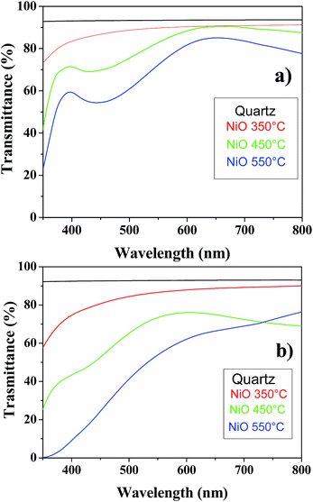 | ||
| Fig. 9 Transmittance spectra of NiO films on quartz from (a) Ni(tta)2·tmeda and (b) Ni(hfa)2·tmeda as a function of temperature. | ||
Thus, films grown from Ni(tta)2·tmeda are more transparent in the visible region than films obtained using Ni(hfa)2·tmeda, consistent with the Raman results that detected large carbon contamination for the latter.
Fig. 10a shows the spectra of the refractive and extinction coefficient derived by the ellipsometric analysis for the NiO film grown at 450 °C from the Ni(tta)2·tmeda.
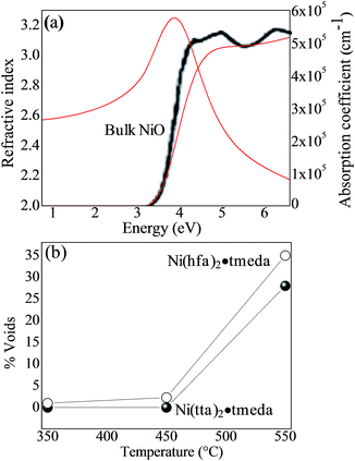 | ||
| Fig. 10 (a) Spectra of the refractive index and absorption coefficient, derived by the ellipsometric analysis, of the NiO film grown on quartz at 450 °C from Ni(tta)2·tmeda. The black-line spectrum refers to single crystal NiO from ref. 50 (b) evolution of the % voids (measure of the film density) as a function of temperature and precursor. | ||
The refractive index at 2 eV of 2.65 is in agreement with that reported for the NiO single crystal.52 The comparison of the spectra of the absorption coefficient also shows a good agreement with the NiO single crystal. The observed slight difference is due to low density of the films due to their polycrystalline structure.53 The densest film was deposited at 450 °C from Ni(tta)2·tmeda; the increase of void fraction in Fig. 10b indicates that the density of the NiO films decreased with the Ni(hfa)2·tmeda precursor and with the increased temperature, consistent with the change in morphology seen in Fig. 7 (larger grains and less compact microstructure were observed with the increase in temperature).
From the (αE)2 vs. energy, E, plot, a direct optical gap of 3.7 eV was estimated that compares well with the 3.8–4.0 eV single crystal NiO value.51
While temperature mainly affected the microstructure and density and consequently the refractive index, it was verified that the optical bandgap was mainly affected by the O2 flow.54
Fig. 11 shows the optical properties in the region of the absorption edge of the NiO films derived by the ellipsometric analysis as a function of O2 flow.
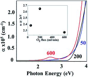 | ||
| Fig. 11 Absorption coefficient around the fundamental absorption edge of NiO films grown on quartz at 50, 200 and 600 sccm O2. | ||
The sharper absorption edge indicated an optimal O2 flow of 200 sccm. An excess of O2 flow (e.g. 600 sccm) caused Ni vacancies that altered the band structure55 and result in a low energy (at 2–3 eV) absorption peak correlated to the nickel 3d8–3d8* transitions. In contrast, a low O2 flow (50 sccm) resulted in O2− vacancies that inhibited the previous peak, but the defects resulted in extended band tail absorption.
Electrical properties and work function of NiO films
The van der Pauw contact geometry has been used to determine resistivity and carrier mobility of NiO films from Ni(tta)2·tmeda, since those were found, from previous characterizations, to be carbon-free and with better crystallinity, transparency and a sharper optical bandgap. Those films showed a resistivity in the 102 to 104 Ω cm range and a carrier mobility below 20 cm2 V−1 s−1, consistent with the film stoichiometry.The work function, WF, of the NiO films was determined, which is important for the performance of OLEDs and solar cells since it determines the energy barrier height at the interface of the anode electrode with the active materials, which concerns the efficiency of hole injection and the operating voltage of the cell. Calibrating our KPFM values against the WF of a reference evaporated gold contact (WF(Au) = 4.75 eV), 5.10 ± 0.05 eV was measured for NiO films deposited from Ni(tta)2·tmeda, consistent with data in the literature with WF values ranging from 3.7 to 6.7 eV.56–59 Fig. 12 compares the WF measured for our NiO films with some WF data from the literature providing a perspective of the complexity in comparing WF data that depend not only on the measurement approach but also on the deposition methodology and conditions.
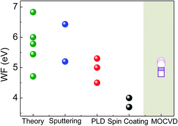 | ||
| Fig. 12 Work functions, WFs, values of the NiO films from MOCVD by Ni(tta)2·tmeda (gray shaded area) compared with theoretical data (green points) [ref. 13 and ref. therein] and experimental data from films deposited by various methodologies of spin coating (black points) [ref. 56a and b], PLD (red points) [ref. 57 and 58] and sputtering (blue points) [ref. 56c and 59]. | ||
Experimental WF values of NiO films deposited by wet- and dry experimental procedures56 are generally lower than those from theory13 because theory does not take into account defects such as oxygen vacancies or surface impurities. The WF of NiO films have been associated with their composition.57 Values larger than 5 eV have been reported for non-stoichiometric NiO films with Ni vacancies and excess oxygen.
Interestingly, in the present case, the films from the Ni(tta)2·tmeda precursor, without any need of additional post-growth treatments, had an approximate 5.1 eV WF, which is suitable for efficient hole extraction at the organic interfaces and could increase the organic photovoltaic device efficiency.56b
Conclusions
Polycrystalline NiO films have been prepared by MOCVD on quartz and single crystal LaAlO3 (001) substrates using two different precursors, Ni(tta)2·tmeda and Ni(hfa)2·tmeda. It was shown that it is possible to tailor the structural, morphological and functional properties of the NiO films by varying the deposition temperature, whose increase improves the crystallinity and the grain size of the films. Deposition temperature played a crucial role not only on the structural but also on the morphological and optical properties in terms of transparency.In particular,
- The crystallinity and grain size improved with increased temperature, being optimal at 550 °C and with the Ni(tta)2·tmeda precursor, yielding cubic NiO.
- The larger crystallinity and grain size obtained from Ni(tta)2·tmeda are consistent with the almost stoichiometric and antiferromagnetic character detected by Raman spectroscopy, which also revealed that strong carbon contamination was induced by Ni(hfa)2·tmeda.
- FE-SEM and AFM analyses indicated that very homogeneous films formed in both cases, although AFM indicated a lower roughness for the NiO from Ni(tta)2·tmeda.
- The optical properties were strictly influenced by all parameters, including the precursor, temperature and O2 flow. In particular, the Ni(tta)2·tmeda precursor results in more transparent and denser NiO films than Ni(hfa)2·tmeda with the transparency decreasing with increased temperature, while the O2 flow had an impact on the sharpness of the optical bandgap, since a non-optimal flow can result in Ni-vacancies and/or oxygen interstitial excess both introducing defect levels below the fundamental gap.
- The NiO films from Ni(tta)2·tmeda showed approximately 5.1 eV work function, indicating that they have potential for use as efficient hole injection layers.
Thus, the Ni(tta)2·tmeda precursor is suitable for MOCVD growth of NiO films with transparency, very low interface roughness and work function and has potential for applications in light-emitting devices19 or photovoltaics.60,61
Acknowledgements
The authors thank the University of Catania for financial support within the FIR project. S. O. thanks the PON A3-00136 BRIT project for economic support for PhD training.References
- D. P. Woodruff, Chem. Rev., 2013, 113, 3863–3886 CrossRef CAS PubMed.
- M. Kandyla, C. Chatzimanolis-Moustakas, E. P. Koumoulos, C. Charitidis and M. Kompitsas, Mater. Res. Bull., 2014, 49, 552–559 CrossRef CAS.
- A. M. Soleimanpour, Y. Hou and A. Jayatissa, Sens. Actuators, B, 2013, 182, 125–133 CrossRef CAS.
- A. Cimino, M. Lo Jacono and M. Schiavello, J. Phys. Chem., 1971, 75, 1044–1050 CrossRef CAS.
- F. Arena, A. Licciardello and A. Parmaliana, Catal. Lett., 1990, 6, 139–149 CrossRef CAS.
- D. T. Gillaspie, R. C. Tenent and A. C. Dillon, J. Mater. Chem., 2010, 20, 9585–9592 RSC.
- K.-K. Chiang and J.-J. Wu, ACS Appl. Mater. Interfaces, 2013, 5, 6502–6507 CAS.
- S. Pereira, A. Goncalves, N. Correia, J. Pinto, L. Pereira, R. Martins and E. Fortunato, Sol. Energy Mater. Sol. Cells, 2014, 120, 109–115 CrossRef CAS.
- R.-T. Wen, G. A. Niklasson and C. G. Granqvist, ACS Appl. Mater. Interfaces, 2015, 7, 9319–9322 CAS.
- J. W. Shim, C. Fuentes-Hernandez, A. Dindar, Y. Zhou, T. M. Khan and B. Kippelen, Org. Electron., 2013, 14, 2802–2808 CrossRef CAS.
- I. Sta, M. Jlassi, M. Hajji and H. Ezzaouia, Thin Solid Films, 2014, 555, 131–137 CrossRef CAS.
- M. D. Irwin, D. B. Buchholz, A. W. Hains, R. P. H. Chang and T. J. Marks, Proc. Natl. Acad. Sci. U. S. A., 2008, 105, 2783–2787 CrossRef CAS.
- M. D. Irwin, J. D. Servaites, D. B. Buchholz, B. J. Leever, J. Liu, J. D. Emery, M. Zhang, J.-H. Song, M. F. Durstock, A. J. Freeman, M. J. Bedzyk, M. C. Hersam, R. P. H. Chang, M. A. Ratner and T. J. Marks, Chem. Mater., 2011, 23, 2218–2226 CrossRef CAS.
- T. Ripolles-Sanchis, A. Guerrero, E. Azaceta, R. Tena-Zaera and G. Garcia-Belmonte, Sol. Energy Mater. Sol. Cells, 2013, 117, 564–568 CrossRef CAS.
- F. Odobel, L. Le Pleux, Y. Pellegrin and E. Blart, Acc. Chem. Res., 2010, 43, 1063–1071 CrossRef CAS PubMed.
- D. Ameline, S. Diring, Y. Farre, Y. Pellegrin, G. Naponiello, E. Blart, B. Charrier, D. Dini, D. Jacquemin and F. Odobel, RSC Adv., 2015, 5, 85530–85539 RSC.
- F. Odobel, Y. Pellegrin, E. A. Gibson, A. Hagfeldt, A. L. Smeigh and L. Hammarstrom, Coord. Chem. Rev., 2012, 256, 2414–2423 CrossRef CAS.
- T. J. Macdonald, Y. J. Mange, M. R. Dewi, H. U. Islam, I. P. Parkin, W. M. Skinner and T. Nann, J. Mater. Chem. A, 2015, 3, 13324–13331 CAS.
- J.-M. Caruge, J. E. Halpert, V. Bulović and M. G. Bawendi, Nano Lett., 2006, 6, 2991–2994 CrossRef CAS PubMed.
- H. Wang, Y. Zhao, C. Wu, X. Dong, B. Zhang, G. Wu, Y. Ma and G. Du, J. Lumin., 2015, 158, 6–10 CrossRef CAS.
- H. P. Rooksby, Nature, 1943, 152, 304 CrossRef CAS.
- N. Mironova-Ulmane, A. Kuzmin, I. Steins, J. Grabis, I. Sildos and M. Pärs, J. Phys.: Conf. Ser., 2007, 93, 012039 CrossRef.
- A. C. Gandhi, J. Pant, S. D. Pandit, S. K. Dalimbkar, T.-S. Chan, C.-L. Cheng, Y.-R. Ma and S. Y. Wu, J. Phys. Chem. C, 2013, 117, 18666–18674 CAS.
- A. C. Gandhi, C.-Y. Huang, C. C. Yang, T. S. Chan, C.-L. Cheng, Y.-R. Ma and S. Y. Wu, Nanoscale Res. Lett., 2011, 6, 485–497 CrossRef PubMed.
- C.-M. Wang, C.-Y. Wen, Y.-C. Chen, S.-Y. Lin and S.-T. Shiau, Adv. Mater.Adv. Mater. Res., 2013, 690–693, 1685–1689 Search PubMed.
- M. Krunks, J. Soon, T. Unt, A. Mere and V. Mikli, Vacuum, 2014, 107, 242–246 CrossRef CAS.
- M. Jlassi, I. Sta, M. Hajji and H. Ezzaouia, Mater. Sci. Semicond. Process., 2014, 21, 7–13 CrossRef CAS.
- Y. Chuminjak, S. Daothong, P. Reanpang, J. P. Mensing, D. Phokharatkul, J. Jakmunee, A. Wisitsoraat, A. Tuantranont and P. Singjai, RSC Adv., 2015, 5, 67795–67802 RSC.
- Y. Zhang and Z. Guo, Chem. Commun., 2014, 50, 3443–3446 RSC.
- M. Z. Sialvi, R. J. Mortimer, G. D. Wilcox, A. M. Teridi, T. S. Varley, K. G. U. Wijayantha and C. A. Kirk, ACS Appl. Mater. Interfaces, 2013, 5, 5675–5682 CAS.
- W.-J. An, E. Thimsen and P. Biswas, J. Phys. Chem. Lett., 2010, 1, 249–253 CrossRef CAS.
- H. Wang, G. Wua, X. P. Cai, Y. Zhao, Z. F. Shi, J. Wang, X. C. Xia, X. Dong, B. L. Zhang, Y. Ma and G. T. Du, Vacuum, 2012, 86, 2044–2047 CrossRef CAS.
- J.-K. Kang and S.-W. Rhee, Thin Solid Films, 2001, 391, 57–61 CrossRef CAS.
- K.-C. Min, M. Kim, Y.-H. You, S. S. Lee, Y. K. Lee, T.-M. Chung, C. G. Kim, J.-H. Hwang, K.-S. An, N.-S. Lee and Y. Kim, Surf. Coat. Technol., 2007, 201, 9252–9255 CrossRef CAS.
- G. Malandrino, L. M. S. Perdicaro, I. L. Fragala, R. Lo Nigro, M. Losurdo and G. Bruno, J. Phys. Chem. C, 2007, 111, 3211–3215 CAS.
- E. Thimsen, A. B. F. Martinson, J. W. Elam and M. J. Pellin, J. Phys. Chem. C, 2012, 116, 16830–16840 CAS.
- P. A. Premkumar, M. Toeller, C. Adelmann, J. Meersschaut, A. Franquet, O. Richard, H. Tielens, B. Brijs, A. Moussa, T. Conard, H. Bender, M. Schaekers, J. A. Kittl, M. Jurczak and S. V. Elshocht, Chem. Vap. Deposition, 2012, 18, 61–69 CrossRef.
- H. Wang, Y. Zhao, X. Li, C. Wu, X. Dong, Y. Ma, B. Zhang and G. Du, Vacuum, 2015, 119, 77–80 CrossRef CAS.
- A. S. Kondrateva, M. Mishin, A. Shakhmin, M. Baryshnikova and S. E. Alexandrov, Phys. Status Solidi C, 2015, 12, 912–917 CrossRef CAS.
- G. Malandrino, L. M. S. Perdicaro, G. Condorelli, I. L. Fragala, P. Rossi and P. Dapporto, Dalton Trans., 2006, 8, 1101–1106 RSC.
- T. Yoshida, M. Oguni, Y. Mori and Y. Fukuda, Solid State Commun., 1995, 93, 159–162 CrossRef CAS.
- (a) W. Melitz, J. Shen, A. C. Kummel and S. Lee, Surf. Sci. Rep., 2011, 66, 1–27 CrossRef CAS; (b) V. Palermo, M. Palma and P. Samorì, Adv. Mater., 2006, 18, 145–164 CrossRef CAS; (c) H. Takano, J. R. Kenseth, S. S. Wong, J. C. O'Brien and M. D. Porter, Chem. Rev., 1999, 99, 2845–2890 CrossRef CAS PubMed.
- T. Filleter, K. V. Emtsev, T. Seyller and R. Bennewitz, Appl. Phys. Lett., 2008, 93, 133117 CrossRef.
- G. E. Jellison Jr, Thin Solid Films, 1993, 234, 416–422 CrossRef.
- (a) G. E. Jellison Jr and F. A. Modine, Appl. Phys. Lett., 1996, 69, 371–373 CrossRef; (b) G. E. Jellison Jr and F. A. Modine, Appl. Phys. Lett., 1996, 69, 2137 CrossRef.
- G. He, L. D. Zhang, G. H. Li, L. Q. Zhu, S. S. Pan and Q. Fang, Appl. Phys. Lett., 2005, 86, 232901 CrossRef.
- D. Brandon and W. D. Kaplan, Microstructural Characterization of Materials, John Wiley & Sons Ltd, Chicester, West Sussex, England, 1999 Search PubMed.
- F. Roccaforte, G. Greco, P. Fiorenza, V. Raineri, G. Malandrino and R. Lo Nigro, Appl. Phys. Lett., 2012, 100, 063511 CrossRef.
- R. Lo Nigro, S. Battiato, G. Greco, P. Fiorenza, F. Roccaforte and G. Malandrino, Thin Solid Films, 2014, 563, 50–55 CrossRef CAS.
- R. Lo Nigro, G. Fisichella, S. Battiato, G. Greco, P. Fiorenza, F. Roccaforte and G. Malandrino, Mater. Chem. Phys., 2015, 162, 461–468 CrossRef CAS.
- S. H. Lee, H. M. Cheong, N. G. Park, C. E. Tracy, A. Mascarenhas, D. K. Benson and S. K. Deb, Solid State Ionics, 2001, 140, 135 CrossRef CAS.
- R. J. Powell and W. E. Spicer, Phys. Rev. B: Solid State, 1970, 2, 2182–2193 CrossRef and reference therein.
- D. Franta, B. Negulescu, L. Thomas, P. R. Dahoo, M. Guyot, I. Ohlidal, J. Mistrik and T. Yamaguchi, Appl. Surf. Sci., 2005, 244, 426–430 CrossRef CAS.
- J. W. Park, K. N. Choi, S. H. Baek, K. S. Chung and H. Lee, J. Korean Phys. Soc., 2008, 52, 1868–1876 CrossRef CAS.
- H. Y. Peng, Y. F. Li, W. N. Lin, Y. Z. Wang, X. Y. Gao and T. Wu, Sci. Rep., 2012, 2, 442 Search PubMed.
- (a) K. X. Steirer, P. F. Ndione, N. E. Widjonarko, M. T. Lloyd, J. Meyer, E. L. Ratcliff, A. Kahn, N. R. Armstrong, C. J. Curtis, D. S. Ginley, J. J. Berry and D. C. Olson, Adv. Energy Mater., 2011, 1, 813–820 CrossRef CAS; (b) B. Mustafa, J. Griffin, A. S. Alsulami, D. G. Lidzey and A. R. Buckley, Appl. Phys. Lett., 2014, 104, 063302 CrossRef; (c) M. T. Greiner, M. G. Helander, Z. B. Wang, W. M. Tang and Z. H. Lu, J. Phys. Chem. C, 2010, 114, 19777–19781 CrossRef CAS.
- T. Dutta, P. Gupta, A. Gupta and J. Narayan, J. Phys. D: Appl. Phys., 2010, 43, 105301 CrossRef.
- (a) J. Olivier, B. Servet, M. Vergnolle, M. Mosca and G. Garry, Synth. Met., 2001, 122, 87–89 CrossRef CAS; (b) J. J. Berry, N. E. Widjonarko, B. A. Bailey, A. K. Sigdel, D. S. Ginley and D. C. Olson, IEEE J. Sel. Top. Quantum Electron., 2010, 16, 1649–1655 CrossRef CAS.
- D. J. Yun and S. W. Rhee, J. Vac. Sci. Technol., B: Microelectron. Nanometer Struct.--Process., Meas., Phenom., 2008, 26, 1787–1793 CrossRef CAS.
- Q. Liu, L. Wei, S. Yuan, X. Ren, Y. Zhao, Z. Wang, M. Zhang, L. Shi, D. Li and A. Li, RSC Adv., 2015, 5, 71778–71784 RSC.
- J. Y. Park, B. Y. Jang, C. H. Lee, H. J. Yun and J. H. Kim, RSC Adv., 2014, 4, 61248–61255 RSC.
| This journal is © The Royal Society of Chemistry 2016 |


