ZnO quantum dots decorated on optimized carbon nanotube intramolecular junctions exhibit superior field emission properties
Chia-Te Hua,
Jyh-Ming Wua,
Jien-Wei Yeha and
Han C. Shih*ab
aDepartment of Materials Science and Engineering, National Tsing Hua University Hsinchu, Taiwan 30013, Republic of China. E-mail: hcshih@mx.nthu.edu.tw
bInstitute of Materials Science and Nanotechnology, Chinese Culture University Taipei, Taiwan 11114, Republic of China
First published on 1st June 2016
Abstract
Highly efficient carbon-based 1D light-emitting devices require multi-quantum well heterostructures with sensitive optical properties. However, carbon nanotubes (CNTs)-based composites become much worse than expected and most of their applications such as field emission are thwarted because dispersing CNTs among one another is difficult. We demonstrate that such sensitive optical and limited field emission properties can be attained and improved, respectively, through the use of ZnO nanocrystal selective quantum well heterostructures grown on carbon nanotubes to fabricate carbon-zinc-oxide (CZO) nanotubes. ZnO can be effectively and uniformly decorated on the carbon nanotubes intramolecular junctions with abundant functional groups and also with large surface adsorption area produced by CNTs surface plasma pre-treatments at room temperature. The cathodoluminescence (CL) spectrum of the CZO nanotubes exhibits a weak UV emission peak and two distinct strong green emission peaks at 2.51 eV and at 2.4 eV, attributed to zinc-rich ZnO band-to-donor transitions and oxygen-rich ZnO band-to-acceptor transitions, respectively. Furthermore, the CZO nanotubes reach an extremely low turn-on field of 0.1 V μm−1, low threshold field of 3.1 V μm−1, but high field enhancement factor β of 110 × 103. The field emission properties are dramatically enhanced by ZnO quantum dots decorated on the carbon nanotube intramolecular junctions, which not only provide extra electron emission paths and higher carrier concentrations, but also protect the emitter from ion bombardment during operation.
1. Introduction
The optical characteristics of semiconductor 1D nanostructures attract a great deal of interest because of their emerging applications in the field of nano-photonics.1,2 The construction of several devices based on nanostructures has already been reported, including that of single photon emitters,3,4 optically and electrically pumped nanowire lasers,5–8 polarization sensitive photodetectors,9 multicolor light emitting diodes,5,10,11 and solar cells.12Because the aggregation of nanotubes into bundled form as well as the intrinsic defects will induce low luminescent efficiency for carbon nanotubes (CNTs). However, the light absorption of the CNTs and its surface geometry materials can be possibly further modified to exhibit superior electrical properties. For instance, a variety of CNTs and nanoparticle hybrid nanomaterials have been synthesized,13–23 mainly achieved by utilizing either covalent or non-covalent binding mechanisms between nanoparticles and CNTs. Nevertheless, the hybrid nanomaterials usually use expensive noble metal particles, such as Pt, Au, Ag, Cd, and Pb, attached to CNTs, which alter both the optical and electric properties of the CNTs.13,24 Moreover, some decorated inexpensive particles are detrimental for synthesizing hybrid nanomaterials. For example, the toxic and harmful properties of cadmium, lead, and their compounds make them unfavorable for the synthesis of eco-friendly nanomaterials. Therefore, it has become critical to have low-cost and environmentally-friendly nanomaterials to replace these expensive or toxic ones. In this respect, some other compounds with properties of relatively inexpensive and harmless nanomaterials, such as CdSe, CdS, PbS, and CuS nanoparticles, have been utilized to replace noble nanoparticles.19,21–23 One of the ideal and promising materials is zinc oxide (ZnO) nanomaterials, which are both eco-friendly and inexpensive materials. ZnO has attracted the attention of many groups working on light emitting devices because of its remarkable optical,25 electronic,26,27 and magnetic properties28 due to its large excitation binding energy (60 meV), direct wide band gap (3.4 eV), and unique piezoelectric properties.29,30 However, the fabrication of ZnO nanocrystals decorated CNTs with well-controlled sizes and good uniformity in the selected area for superior field emission properties still remains a challenge.
In principle, it is feasible to make use of CNTs with high degree of graphitization and high surface adsorption ability as 1D hard template to impart high stability of ZnO deposition. One of the most appropriate structures is carbon nanotube intramolecular junctions, which are formed by bringing pentagon–heptagon rings together. Many theoretical studies on the electronic31–38 and optical39 properties of the intramolecular junctions have been carried out to indirectly obtain detailed information on their topological structures. In this study, we devise a method to create this type of structure by a simple procedure that not only allows creating of the structures at room temperature, but also permits occurrence of designed graphitic shapes and structures.
On the other hand, CNTs satisfy most of the requirements as a good field emitter, such as low field emission threshold (9.8 V μm−1),40 high current density and good emission homogeneity. However, there exist many conjugated structures and strong van der Waals interactions among CNTs; therefore, it is difficult to disperse CNTs among each other. As a result, the properties of the CNT-based composites become much worse than expected and most of their applications, such as capacitive materials and field emission, are thwarted by this drawback. In this study, we demonstrated that the ZnO nanocrystal decorated CNTs exhibit unique optical properties and extremely low threshold field. Moreover, the model of the growth mechanism and enhancement of field emission properties will be clearly discussed.
2. Experimental
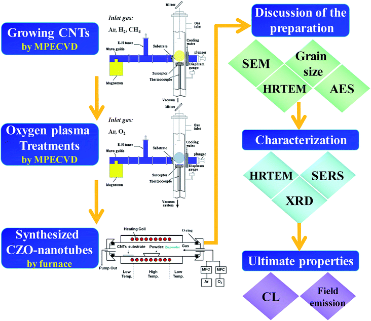
The process flow diagram for CZO nanotubes production is outlined in Fig. 1. In this study, microwave plasma enhanced chemical vapor deposition (MPECVD) was used to synthesize CNTs. An iron-containing compound was used as the catalyst, which was first coated onto an Al2O3 substrate using a sol–gel method to promote the growth of CNTs. The substrate was placed in the MPECVD chamber, where a gas mixture of methane and hydrogen (1![[thin space (1/6-em)]](https://www.rsc.org/images/entities/char_2009.gif) :
:![[thin space (1/6-em)]](https://www.rsc.org/images/entities/char_2009.gif) 10) was introduced and simultaneously decomposed by the microwaves to synthesize the carbon-related materials. During this period, the pressure was maintained at 20 Torr with a microwave power of 1.5 kW at 650 °C as measured by a thermocouple (CA).
10) was introduced and simultaneously decomposed by the microwaves to synthesize the carbon-related materials. During this period, the pressure was maintained at 20 Torr with a microwave power of 1.5 kW at 650 °C as measured by a thermocouple (CA).
After growth of the CNTs, the microwave chamber was cooled down to room temperature and surface modification treatment subsequently started. The plasma treatments by oxygen gas source for the MWCNTs were conducted under the following conditions: gas flow rate of 20 sccm, operating pressure of 0.5 Torr, microwave power of 600 W, process duration of 5–35 s, and average sample temperature of about 30 °C.
The ZnO nanocrystals then were deposited onto the surface of CNTs through a vapor–liquid–solid (VLS) method. Metallic zinc with a purity of 99.9% was taken from the source material. The source material (0.5 g) was placed in front of the alumina boat. The boat was then loaded onto the center of a horizontal Mullite tube (Al2O3) with an inner diameter of 65 mm and a length of 120 cm, mounted in an electric tube furnace. The temperature was increased to 600 °C under a working pressure of 1 Torr with a constant argon flow at 100 sccm. During synthesis, the furnace was maintained at these temperatures for 60 min in a flow of 100 sccm argon and 5 sccm oxygen, which were introduced as a gaseous mixture. Subsequently, the furnace naturally cooled down to room temperature and gray nanocomposite products were found on the Si substrates.
The surface morphology and microstructural characterizations were carried out by field emission scanning electron microscopy (FE-SEM, JSM-6500F) and high-resolution transmission electron microscopy (HRTEM, JEOL JEM-2010, 200 kV). For phase identification, the structure characterization was performed using X-ray diffraction (XRD, Osmic PSAXS-USH-WAXS-002). Composition mapping of the single CZO nanotube in the lateral direction was analyzed by an Auger electron nanoscope (Nano-Auger, ULVAC-PHI, PHI 700). An ultrasensitive technique of surface enhanced Raman scattering (SERS)41–45 satisfies the requirement for probing vibrational modes associated with topological defects, due to the huge enhancement of the Raman cross-section in the vicinity of metal surfaces. The optical properties based on the band structure were analyzed by the cathodoluminescence (CL) measurements at room temperature. The CL spectrum of the CZO nanotubes was measured by a spatially resolved CL system (Gatan Mono CL3, integrated with a field-emission SEM, JEOL JSM-6500F, 20 keV). The electron field emission characteristics of CZO nanotubes were measured by the conventional diode method in a vacuum chamber with 1 × 10⁻⁶ Torr. The current density and the electric field (J–E) characteristics were measured using an electrometer (Keithley 237). The field-emission measurements were carried out using a parallel plate structure with the CZO nanotubes as the cathode and an indium-tin-oxide (ITO) coated glass as the anode. The distance between two electrodes was estimated as 42 μm by a glass fiber spacer and the measured emission area was 1 mm2.
3. Results and discussion
Part I: discussion of the preparation
Fig. 2 shows the scanning electron microscope SEM images of the final CZO nanotubes obtained by different oxygen plasma pre-treatments. Fig. 2(a)–(d) represent 0, 5, 20, and 35 s of oxygen plasma pre-treatments times, as named by A, B, C, and D, respectively. It is clear that four different types of morphology and growth site densities of nanocrystals were observed. Fig. 2(c) reveals a clearly hexagonal architecture of nanocrystals connected with each other, indicating the wurtzite structure of ZnO. A characteristic HRTEM image of the obtained CZO nanotube reveals a preferred growth in the [0001] direction, a single-crystal structure of hexagonal wurtzite ZnO with a clear lattice fringe of 0.51 nm, and CNT inner diameters of 0.35 nm. After a rare treatment for 5 s on the CNTs surface, a few small sized ZnO grow across the walls of the CNTs, as shown in Fig. 2(e). When increasing the treatment time to 20 s, as shown in Fig. 2(f), ZnO grows upwards to uniformly cover all the CNTs and enlarge the size at the same time, which was in agreement with SEM results. The ZnO nanocrystal size reached a critical point in the 20 s oxygen plasma treatment at a maximum size of about 40 nm and minimum coefficient of variation of about 9.7%, as shown in the Fig. 3 box plot and histogram. As a result, the formation of CZO nanotubes not only alters the crystallization of ZnO, but also maintains the hollow tubular structure of the carbon nanotubes. On the other hand, the deposition of ZnO nanocrystals left no trace on the silicon base substrate unless there were treated CNTs.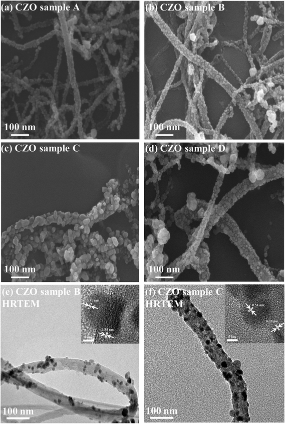 | ||
| Fig. 2 SEM images of CZO nanotubes produced under different oxygen plasma pre-treatments of CNTs for (a) 0, (b) 5, (c) 20, (d) 35 seconds, and TEM images with HRTEM insets for (e) 5, (f) 20 seconds. | ||
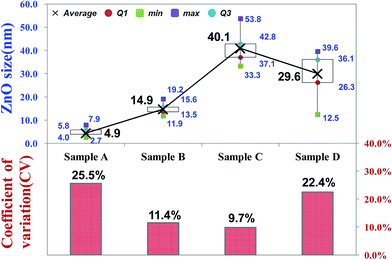 | ||
| Fig. 3 Box plot for grain size and histogram for coefficient of variation sampling from SEM observation. | ||
To determine the chemical composition of a single CZO nanotube precisely, AES (Auger Electron Spectroscopy) was used to study the surface composition of the as-synthesized materials. In Fig. 4, the solid line shows the AES survey, which corresponded to the SEM images inserted beside each point of each plasma treatment condition. The element composition of two points with the same CZO nanotubes was measured by AES. The experiment results revealed the existence of carbon, zinc, oxide, and a minute quantity of Fe elements. No obvious peaks for other elements or impurities were observed. The highest atomic proportion of zinc and oxygen was about 47.7 at% and 46.3 at%, whereas the lowest atomic proportion of carbon was about 6.0 at% in sample C due to ZnO fully covering the surface of CNTs, corresponding to the SEM morphology results shown in Fig. 2(c). It is notable that the proportion of ZnO deposition on the CNTs has a significant upward trend with increasing oxygen plasma treatment time in the first 20 s. A possible reason is that oxygen plasma modified the surface absorption situation of CNTs; therefore, ZnO could easily nucleate and grow via those activated sites, which might result in the strong increase in the ratio of Zn and O elements. The deviation of the atomic percentage, average grain size and ZnO chemical composition by different conditions of CZO nanotubes are summarized in Table 1. These findings are in good agreement with those of our previous studies on a CNTs gas sensor.46 On the basis of the nano-AES result, the atomic ratio of Zn![[thin space (1/6-em)]](https://www.rsc.org/images/entities/char_2009.gif) :
:![[thin space (1/6-em)]](https://www.rsc.org/images/entities/char_2009.gif) O is 1.03
O is 1.03![[thin space (1/6-em)]](https://www.rsc.org/images/entities/char_2009.gif) :
:![[thin space (1/6-em)]](https://www.rsc.org/images/entities/char_2009.gif) 1, which is almost a stoichiometric ZnO compound.
1, which is almost a stoichiometric ZnO compound.
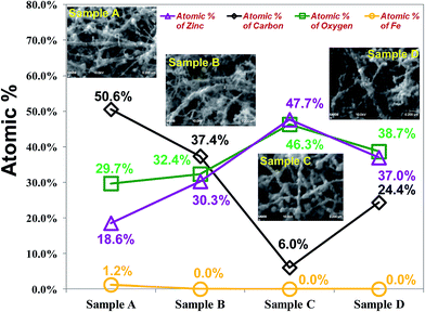 | ||
| Fig. 4 Single CZO nanotube component analysis of different pre-treatment conditions. Insets show SEM images achieved from AES measurement. | ||
| Condition | Atomic% of Fe | Atomic% of carbon | Atomic% of oxygen | Atomic% of zinc | ZnO chemical composition | ZnO size (nm) |
|---|---|---|---|---|---|---|
| a CZO component and grain size analysis of the samples A–D. | ||||||
| Sample A | 1.2% | 50.6% | 29.7% | 18.6% | 0.62 | 4.9 |
| Sample B | 0.0% | 37.4% | 32.4% | 30.3% | 0.94 | 14.9 |
| Sample C | 0.0% | 6.0% | 46.3% | 47.7% | 1.03 | 40.1 |
| Sample D | 0.0% | 24.4% | 38.7% | 37.0% | 0.96 | 29.6 |
Part II: characterization
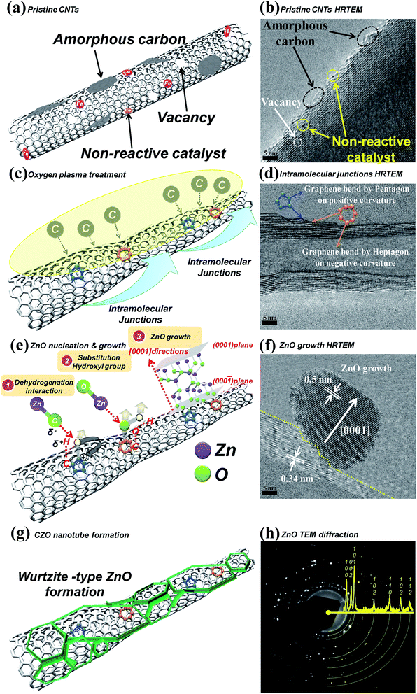
A good understanding of the mechanism of ZnO materials formation on the CNTs is critically necessary for future investigations into this new class of heterostructures. The energetically preferred selected-area growth continued by the thermodynamic mechanism was proposed by Jena et al.47 and Porter et al.,48 who reported that crystalline materials invariably contain dislocations, grain boundaries, and interface energy. All these, which are associated with potentially positive free energy, are responsible for the high surface energy, acting as nucleation sites for crystal growth. Therefore, increasing the content of functional groups or surface adsorption area on the samples is a feasible way to enhance Zn nucleation density and loading amount. On the basis of the following discussion, the growth process of ZnO nanocrystals can be illustrated in Fig. 5.It is clear that defects are always present within the CNTs, as shown in Fig. 5(a), and the amount of defects depends on the production method by MPECVD, which involves lower process temperatures of about 500–700 °C. These pristine CNTs contain a large number of vacancies, amorphous carbons, and non-reactive catalysts that would further decrease the chemical activity of ZnO nucleation and growth, as shown by the HRTEM analysis in Fig. 5(b). After introducing the appropriate amount of oxygen plasma, it has not only reduced these inactive defects, but also re-broken and re-established carbon atoms on the surface of the graphene structure to form sp2 and dangling bonds. The existence of sp2 and dangling bonds seems crucial to the most important architecture, i.e., C–C nanotube intramolecular junctions led by pentagon–heptagon rings which connect the intra-graphene structure, as shown in Fig. 5(c). Pentagons, hexagons, and heptagons were major structures of the surface graphene throughout the nanotube intramolecular junctions growing process, the growth mechanism of which has been simulated by Jianbing et al.,49 and Ziwei et al.50 Both pentagons and heptagons were located in important positions that made intra-graphene connected to each other to re-establish stepped structures, which strongly enhanced the activation energy of the sites and surface adsorption areas for bonding with elements that we wanted. However, the difference is that pentagons induce positive curvature, whereas heptagons induce negative curvature, as shown in Fig. 5(d). Furthermore, sp3 bonds were observed in each junction point of intra-graphene, but the number of bonds was low during CNTs growth. After stepped-type nanotube intramolecular junctions formation, there was a large amount of C–H and C–OH radical groups on the surface, resulting from H2O species present as a residue on the quartz reactor used in ZnO thermal evaporation. These functional groups led to the constitution of hexagonal ZnO crystals composed of four-fold tetrahedral-coordinated O2− and Zn2+ stacked alternatively along the c-axis, i.e., the [0001] direction, as shown in Fig. 5(e) and (f). Finally, with a continuous supply of reactant Zn vapor and oxygen flow, rapid increase of oxygen pressure resulted in fast growth rate of CZO nanotubes to fully cover the wurtzite-type ZnO nanocrystals in Fig. 5(g). Fig. 5(h) shows the TEM diffraction and XRD pattern corresponding to (100), (002), (101), (102), (110), (103), and (112) plane reflections, indicating formation of wurtzite-type ZnO.
Herein, we demonstrate an experimental way to probe the vibrational properties of pentagon and heptagon defects in nanotube intramolecular junctions using surface-enhanced Raman scattering (SERS), as shown in Fig. 6. All Raman spectra were carried out at ambient temperature in vacuum with the 514 nm line from an Ar+ laser (LABRAM HR 800 UV). It was found that the Raman peaks induced by pentagon defects lay outside of the G-band at 1800, 1835, 1940, and 2014 cm−1 on the surface intra-graphene connection under 5 s oxygen plasma treatment. Furthermore, an additional peak appeared at 2010 cm−1 when plasma treatment was continued after 20 s, which strongly agrees with the calculated Raman spectrum of the pentagon that predicts peaks at 1813, 1849, 1948, 2022, and 2024 cm−1 reported by Toshihiko Fujimori et al.51,52 On the other hand, those of the heptagon are predicted at 1102–1119, 1149–1174, 1370–1382, 1452, and 1494 cm−1,51,52 corresponding to this experiment, which reveals peaks located at 1360–1372, 1442, and 1484 cm−1 under 5 s treatment and additional peaks for 1092–1109 and 1139–1164 cm−1 under 20 s treatment, respectively. The heptagon defect can be regarded as the “heavy-mass” impurity52 in the traditional mass-impurity model, which mainly causes phase shift of vibrational modes. On the opposite end, the pentagon defect can be considered to be the “light-mass” impurity.52 Therefore, the atomic vibration of the heptagon defect is found to be much weaker than those in the pentagon defect, which induced weaker Raman intensities. However, rapid decrease of pentagons and only a broad D band centered at 1273–1374 cm−1 were observed while treatment was continuously applied for about 35 s. The inordinate oxidation process caused nano-windows on the carbon nanostructures,53 mainly opening around the geometrical region near pentagons or heptagons. A hypothesis that localized vibrational modes of the pentagon or heptagon are quenched when the “nano-windows” are generated could explain the disappearance of the Raman signals, which are assigned as localized modes on the pentagons and heptagons. As in our previous analysis of nano-Auger electron spectroscopy and SEM results, two interesting phenomena can be explained by the CZO nanotubes growth mechanism. The first is that deposition of ZnO nanocrystals left no trace on the silicon base substrate unless there were treated CNTs due to lower free energy and higher surface energy acting as nucleation sites for CZO growth. The second is that ZnO crystal size and portion of Zn and oxygen elements increased gradually when the plasma treatment time was from 0 to 20 s due to surface activation energy being increased by higher chemical activity of pentagons and heptagons. The absorption area was also enlarged by nanotube intramolecular junction formation. However, the excessive oxygen plasma treatment of 35 s will cause nano-windows53 and disrupt surface activated sites to inhibit ZnO growth and decrease grain size.
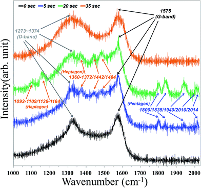 | ||
| Fig. 6 Selected SERS spectra for CNTs under different oxygen plasma pre-treatments for 0, 5, 20, 35 seconds. | ||
Part III: ultimate properties
Cathodoluminescence (CL) spectra taken from the CZO nanotubes at room temperature showed three distinct emission peaks at 376 nm, 494 nm, and 516 nm, as shown in Fig. 7. There are no conspicuous optical peaks for the pristine CNTs, CZO nanotubes sample A, or sample B, which indicates that only a few zinc oxide structures that exhibit non-luminous characteristics were grown. CZO nanotubes sample C shows a strong green emission peak at 494 nm (2.51 eV) and a weak UV emission peak at 376 nm (3.3 eV). After increasing the treatment time of oxygen plasma to 35 s for sample D, the spectrum intensity decreased and the peak shifted to 516 nm (2.4 eV) of green emission; however, the UV peak maintained the same location.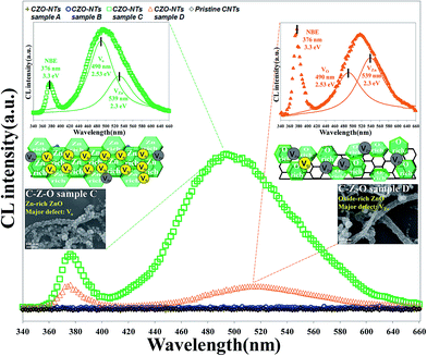 | ||
| Fig. 7 Cathodoluminescence spectrums for pristine CNTs and CZO nanotubes under different oxygen plasma pre-treatments for 0, 5, 20, 35 seconds. | ||
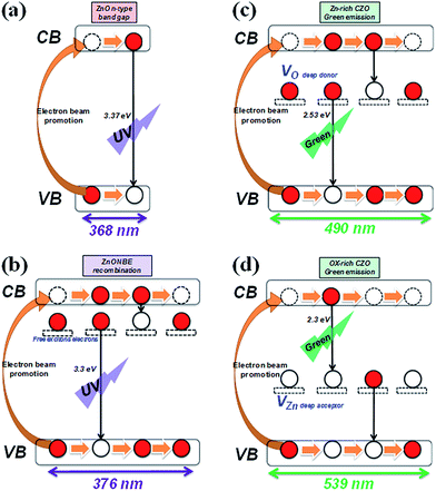
Fig. 8(a) shows the luminescent mechanism for a ZnO n-type semiconductor with wide band gap energy of 3.37 eV at room temperature. The UV emission peak at 376 nm (3.3 eV) corresponds to the near band edge (NBE) peak that is responsible for the recombination of free ZnO excitons like electrons, as Fig. 8(b) shows. The unaltered UV peak position demonstrates that there is no significant mutation in the ZnO crystal structure when fabricating CZO nanotubes under various oxygen pre-treatments, unlike the doping mechanism, which will affect crystal structure. The green emission of 450–600 nm is usually believed to be related to the intrinsic defect structures attributed to several native defects, including interstitials (Zni, Oi),54 antisites (ZnO, OZn),55 zinc vacancies (VZn),56 and oxygen vacancies (VO).57 Along with a particular study reported by C. Ton-That,58 the characteristics of responsible defect centers in Zn-rich and O-rich ZnO are based on a theoretical model of competitive recombination processes. The research shows that nonstoichiometric ZnO exhibits characteristic emissions at 2.53 eV, representing a VO intrinsic defect, and 2.30 eV, representing a VZn intrinsic defect. Compared to the experimental results in this study, it can be concluded that green luminescence at 2.51 eV was mostly contributed by VO in the CZO nanotubes sample C, as shown in Fig. 8(c), and 2.4 eV was mostly contributed by VZn in the CZO nanotubes sample D, as shown in Fig. 8(d). VO and its complexes are all believed to be deep donors in ZnO, whereas VZn is considered to be an acceptor.59 The phenomenon of green emission intensity in CZO nanotubes sample C is much greater than that in CZO nanotubes sample D, which can be explained by deep-donor concentration in Zn-rich ZnO being estimated to be three orders of magnitude greater than deep-acceptor concentration in O-rich ZnO.58
It is important to investigate exhaustively how to generate related intrinsic defects in each plasma modification conditions. From previous analysis, suitable oxygen plasma modification exerted on the surface of the CNTs can not only remove impurities, but also increase activated sites and functional groups. The action will efficiently enhance Zn-rich ZnO growth. On the other hand, redundant ion bombardments may cause creation of dangling bonds and transient polygon carbon rings like octagons,49 which lead to gas adsorption dropping dramatically, thus inhibiting ZnO growth. Furthermore, the amount of oxygen radical species increased gradually under the abundant O2 atmosphere, which resulted in the generation of O-rich and small sized ZnO. This is in a good agreement with the SEM observations of the ZnO grain size following the oxygen plasma treatment order 20 s > 35 s > 5 s > 0 s and the elemental composition having a critical point at 20 s plasma treatment in nano-Auger analysis. The comparative study of CL measurements between CZO nanotubes with different treatment conditions demonstrate that the optical properties can be modified by altering oxygen deficiencies and Zn deficiencies. In this study, we find out a solution to combine these two most promising materials for fabrication of optoelectronic devices operating in the UV and green regions. We believe these nanocomposites could be used as light-emitting devices in nanoscale optoelectronic applications.
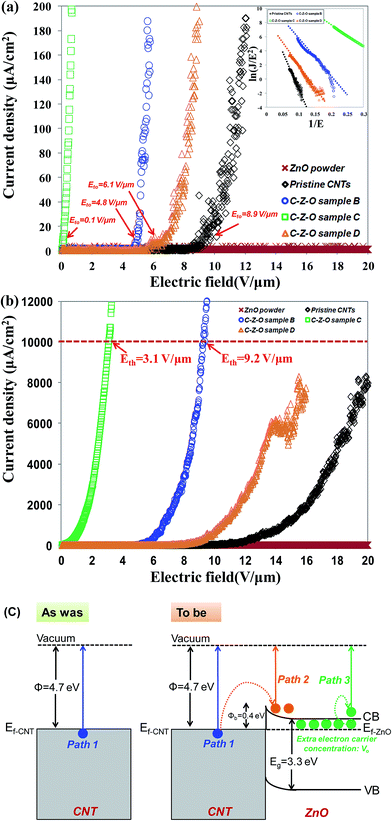
The dependency of the field emission current density on the applied electric field (J–E) between the anode and cathode is shown in Fig. 9 for pristine CNTs, ZnO nanopowders, and CZO nanotubes emitters. The turn-on electric fields Eto are defined as the E values when J reaches 10 μA cm−2, as shown in Fig. 9(a), and the threshold electric fields Eth are defined as the E values when J reaches 10 mA cm−2, as shown in Fig. 9(b). There are no field emission properties for the materials that only include ZnO powders as the control group. A major breakthrough of this study was finding that CZO nanotubes could improve field emission performance significantly for the hybrid emitters in comparison to that of pristine CNTs. To better understand the emission current density against electric field characteristics, this study also analyzes the current–voltage (I–V) data by applying the Fowler–Nordheim (F–N) equation; observe eqn (2), which is the (F–N) natural logarithm equation:60,61
 | (1) |
 | (2) |
After an overall analysis, it can be found that the field emission properties of CZO nanotubes are significantly improved by introducing oxygen plasma from 0 to 20 s. When excessive oxygen plasma was introduced, the current density became unstable and fluctuated; moreover, it reached the limit of about 8000 μA cm−2, which is far lower than the 10![[thin space (1/6-em)]](https://www.rsc.org/images/entities/char_2009.gif) 000 μA cm−2 defined as Eth, as shown in Fig. 9(b). It can be assumed that the generation of destructive structures, such as octagons and oxygen species, on CNTs and incomplete coverage of ZnO cause a screening effect that induced field emission current deviation. On the other hand, the pristine CNTs contain a high degree of impurities and tubes bundled by each other that also make it difficult for field emission properties to reach the threshold current limit. A lower turn-on field, a lower threshold field, and good stability of ZnO nanocrystals grown on nanotube intramolecular junctions for CZO sample C are correlated with not only high field enhancement factor of the emitters, but also tunneling of electrons through surface graphene. The variation of field emission properties can be more concretely analyzed via a band diagram in Fig. 9(c). The interface of CZO nanotubes can be considered to be a metal-semiconductor junction, since the band gap of CNTs is much narrower than that of ZnO.62 Under the external field conditions, the electron emissions can be summarized as three paths. The first path is the injection of electrons to overcome the work function of 4.7 eV from the original CNTs surface. In the second path, electrons are injected from the Fermi level of a CNT into the conduction band of ZnO through tunneling because of the Schottky barrier established at the interface of CZO nanotubes. These electrons are transported to the ZnO surface and are emitted to the vacuum through subsequent tunneling. The Schottky barrier energy level of CZO nanotubes is 0.4 eV, which is shallow enough to allow easy electron transport. High coverage rate and uniform distribution of ZnO, which include abundant VO concentration as extra donor sources, contribute to the third path. These lead to more electrons to emit from the ZnO–vacuum interface under high electric field, in addition to the electrons injected from CNTs into the conduction band of ZnO. On the other hand, ZnO has excellent chemical stability and can protect the emitter from ion bombardment during operation. Thus a high field emission current stability is sustained for CZO nanotubes. Moreover, the ZnO nanocrystals on the surface of nanotube intramolecular junctions can act as additional emission sites, because their small sizes and 1D nature leave many small and sharp tips, leading to an enhanced local field at the tip region.63 Furthermore, in comparison with other nanostructures, such as CNTs,40 ZnO nanowires,64 Ga-doped ZnO nanowires,65 WO3 nanowires,66 AlN nanotips,67 and SiC nanowires,68 listed in Table 2, our CZO nanotubes have the lowest turn-on electric field, the lowest threshold field, and the largest field-enhancement factor β. Different field emission properties and stability for CZO nanotubes were modulated by controlling different internal carrier concentrations from ZnO. These fully integrated the advantages of two different types of materials of high electrical speed of CNTs and excellent sophisticated emission of ZnO.
000 μA cm−2 defined as Eth, as shown in Fig. 9(b). It can be assumed that the generation of destructive structures, such as octagons and oxygen species, on CNTs and incomplete coverage of ZnO cause a screening effect that induced field emission current deviation. On the other hand, the pristine CNTs contain a high degree of impurities and tubes bundled by each other that also make it difficult for field emission properties to reach the threshold current limit. A lower turn-on field, a lower threshold field, and good stability of ZnO nanocrystals grown on nanotube intramolecular junctions for CZO sample C are correlated with not only high field enhancement factor of the emitters, but also tunneling of electrons through surface graphene. The variation of field emission properties can be more concretely analyzed via a band diagram in Fig. 9(c). The interface of CZO nanotubes can be considered to be a metal-semiconductor junction, since the band gap of CNTs is much narrower than that of ZnO.62 Under the external field conditions, the electron emissions can be summarized as three paths. The first path is the injection of electrons to overcome the work function of 4.7 eV from the original CNTs surface. In the second path, electrons are injected from the Fermi level of a CNT into the conduction band of ZnO through tunneling because of the Schottky barrier established at the interface of CZO nanotubes. These electrons are transported to the ZnO surface and are emitted to the vacuum through subsequent tunneling. The Schottky barrier energy level of CZO nanotubes is 0.4 eV, which is shallow enough to allow easy electron transport. High coverage rate and uniform distribution of ZnO, which include abundant VO concentration as extra donor sources, contribute to the third path. These lead to more electrons to emit from the ZnO–vacuum interface under high electric field, in addition to the electrons injected from CNTs into the conduction band of ZnO. On the other hand, ZnO has excellent chemical stability and can protect the emitter from ion bombardment during operation. Thus a high field emission current stability is sustained for CZO nanotubes. Moreover, the ZnO nanocrystals on the surface of nanotube intramolecular junctions can act as additional emission sites, because their small sizes and 1D nature leave many small and sharp tips, leading to an enhanced local field at the tip region.63 Furthermore, in comparison with other nanostructures, such as CNTs,40 ZnO nanowires,64 Ga-doped ZnO nanowires,65 WO3 nanowires,66 AlN nanotips,67 and SiC nanowires,68 listed in Table 2, our CZO nanotubes have the lowest turn-on electric field, the lowest threshold field, and the largest field-enhancement factor β. Different field emission properties and stability for CZO nanotubes were modulated by controlling different internal carrier concentrations from ZnO. These fully integrated the advantages of two different types of materials of high electrical speed of CNTs and excellent sophisticated emission of ZnO.
| Nanostructure | Eto (V μm−1) | Eth (V μm−1) | β (× 103) | Reference |
|---|---|---|---|---|
| a Comparison of field emission characteristics with recent published literature. (Note: Eto: the turn-on electric field; Eth: the threshold electric field; and β: the field enhancement factor). | ||||
| CZO sample C (oxygen plasma pretreat 20 s) | 0.1 | 3.1 | 110.1 | In this paper |
| CNTs | 6.5 | 9.8 | 2.4 | 40 |
| ZnO nanowires | 6.0 | 11.0 | 0.9 | 64 |
| Ga-doped ZnO nanowires | 3.4 | 5.4 | 5.9 | 65 |
| WO3 nanowires | 6.4 | 9.4 | 0.7 | 66 |
| AlN nanotips | 4.7 | 10.6 | 1.2 | 67 |
| SiC nanowires | 5.0 | 8.5 | 0.8 | 68 |
4. Conclusion
An appropriate oxygen plasma treatment not only removes surface impurities of CNTs, but also produces nanotube intramolecular junctions that strongly enhance the activation energy of the site and surface adsorption area. Therefore, CZO nanotubes, which include the largest ZnO nanocrystals, an ideal chemical composition of ZnO, and the most abundant carrier concentrations could be generated under 20 s oxygen plasma pre-treatments. The CL spectrums of these CZO nanotubes exhibit a weak UV emission peak and two distinct strong green emission peaks. The behaviors of the CL emissions at 2.51 eV in Zn-rich ZnO and at 2.4 eV in O-rich ZnO are consistent with band-to-donor and band-to-acceptor transitions, respectively, which could be attributed to increase in the amount and surface coverage degree of ZnO on CNTs. Furthermore, CZO nanotubes provide extra paths and higher carrier concentrations to emit electrons even though the nanostructures are bundled by each other. The field emission measurements confirm that CZO nanotubes have a lower turn-on field of 0.1 V μm−1, a lower threshold field of 3.1 V μm−1, and a larger field enhancement factor β of 110 × 103. On the other hand, ZnO nanocrystals can also protect the emitter from ion bombardment during the operation and act as additional emission sites because of their small sizes and 1D nature. These results indicate that CZO nanotubes can be used in further fundamental research on 1-D nanostructures and technological applications in optoelectronic and field-emission nanodevices.Acknowledgements
This study was sponsored by the National Science Council of the Republic of China (Taiwan) under grant NSC-102-2221-E-034-003.References
- Y. Huang, X. Duan and C. M. Lieber, Small, 2005, 1, 142 CrossRef CAS PubMed.
- P. J. Pauzauskie and P. Yang, Mater. Today, 2006, 9, 36 CrossRef CAS.
- M. T. Borgström, V. Zwiller, E. Müller and A. Imamoglu, Nano Lett., 2005, 5, 1439 CrossRef.
- M. E. Reimer, M. P. V. Kouwen, M. Barkelid, M. Hocevar, M. H. M. V. Weert, R. E. Algra, E. P. A. M. Bakkers, M. T. Björk, H. Schmid, H. Riel, L. P. Kouwenhoven and V. Zwiller, J. Nanophotonics, 2011, 5, 053502 CrossRef.
- F. Qian, Y. Li, S. Gradečak, H. G. Park, Y. Dong, Y. Ding, Z. L. Wang and C. M. Lieber, Nat. Mater., 2008, 7, 701 CrossRef CAS PubMed.
- X. Duan, Y. Huang, R. Agarwal and C. M. Lieber, Nature, 2003, 421, 241 CrossRef CAS PubMed.
- M. H. Huang, S. Mao, H. Feick, H. Yan, Y. Wu, H. Kind, E. Weber, R. Russo and P. Yang, Science, 2001, 292, 1897 CrossRef CAS PubMed.
- S. Gradečak, F. Qian, Y. Li, H. G. Park and C. M. Lieber, Appl. Phys. Lett., 2005, 87, 173111 CrossRef.
- S. Thunich, L. Prechtel, D. Spirkoska, G. Abstreiter, A. F. I. Morral and A. W. Holleitner, Appl. Phys. Lett., 2009, 95, 083111 CrossRef.
- X. Duan, Y. Huang, Y. Cui, J. Wang and C. M. Lieber, Nature, 2001, 409, 66 CrossRef CAS PubMed.
- F. Qian, Y. Li, S. Gradečak, D. Wang, C. J. Barrelet and C. M. Lieber, Nano Lett., 2004, 4, 1975 CrossRef CAS.
- B. Tian, X. Zheng, T. J. Kempa, Y. Fang, N. Yu, G. Yu, J. Huang and C. M. Lieber, Nature, 2007, 449, 885 CrossRef CAS PubMed.
- D. Eder, Chem. Rev., 2010, 110, 1348 CrossRef CAS PubMed.
- J. Y. Kim, J. W. Jang, D. H. Youn, J. Y. Kim, E. S. Kim and J. S. Lee, RSC Adv., 2012, 2, 9415 RSC.
- H. A. Park, S. Liu, P. A. Salvador, G. S. Rohrer and M. F. Islam, RSC Adv., 2016, 6, 22285 RSC.
- W. Haider, A. Hayat, Y. Raza, A. A. Chaudhry, I. U. Rehman and J. L. Marty, RSC Adv., 2015, 5, 24853 RSC.
- U. Jain, J. Narang, K. Rani, Burna, Sunny and N. Chauhan, RSC Adv., 2015, 5, 29675 RSC.
- Y. F. Zhu, Q. Q. Ni and Y. Q. Fu, RSC Adv., 2015, 5, 3748 RSC.
- X. Li, Y. Jia and A. Cao, ACS Nano, 2010, 4, 506 CrossRef CAS PubMed.
- M. Shim, A. Javey, N. W. S. Kam and H. Dai, J. Am. Chem. Soc., 2001, 123, 11512 CrossRef CAS PubMed.
- C. Ratanatawanate, A. Chyao and K. J. Balkus Jr, J. Am. Chem. Soc., 2011, 133, 3492 CrossRef CAS PubMed.
- L. Yang, S. Luo, R. Liu, Q. Cai, Y. Xiao, S. Liu, F. Su and L. Wen, J. Phys. Chem. C, 2010, 114, 4783 CrossRef CAS.
- Y. H. Tseng, Y. He, S. Lakshmanan, C. Yang, W. Chen and L. Que, Nanotechnology, 2012, 23, 455708 CrossRef PubMed.
- P. C. Ma, B. Z. Tang and J. K. Kim, Carbon, 2008, 46, 1497 CrossRef CAS.
- R. Thierry, G. Perillat-Merceroz, P. H. Jouneau, P. Ferret and G. Feuillet, Nanotechnology, 2012, 23, 085705 CrossRef CAS PubMed.
- D. L. Son, B. W. Kwon, D. H. Park, W. S. Seo, Y. Yi, B. Angadi, C. L. Lee and W. K. Choi, Nat. Nanotechnol., 2012, 7, 465 CrossRef CAS PubMed.
- J. S. Liu, C. X. Shan, H. Shen, B. H. Li, Z. Z. Zhang, L. Liu, L. G. Zhang and D. Z. Shen, Appl. Phys. Lett., 2012, 101, 011106 CrossRef.
- G. T. Rao, R. J. Stella, B. Babu, K. Ravindranadh, C. V. Reddy, J. Shim and R. V. S. S. N. Ravikumar, Mater. Sci. Eng., B, 2015, 201, 72 CrossRef CAS.
- Ü. Özgür, Y. I. Alivov, C. Liu, A. Teke, M. A. Reshchikov, S. Doğan, V. Avrutin, S. J. Cho and H. Morkoç, J. Appl. Phys., 2005, 98, 041301 CrossRef.
- Z. L. Wang, Mater. Sci. Eng., R, 2009, 64, 33 CrossRef.
- B. I. Dunlap, Phys. Rev. B: Condens. Matter Mater. Phys., 1994, 49, 5643 CrossRef CAS.
- J. C. Charlier, T. W. Ebbesen and P. Lambin, Phys. Rev. B: Condens. Matter Mater. Phys., 1996, 53, 11108 CrossRef CAS.
- L. Chico, V. H. Crespi, L. X. Benedict, S. G. Louie and M. L. Cohen, Phys. Rev. Lett., 1996, 76, 971 CrossRef CAS PubMed.
- R. Saito, G. Dresselhaus and M. S. Dresselhaus, Phys. Rev. B: Condens. Matter Mater. Phys., 1996, 53, 2044 CrossRef CAS.
- V. Meunier, P. Senet and P. Lambin, Phys. Rev. B: Condens. Matter Mater. Phys., 1999, 60, 7792 CrossRef CAS.
- M. S. Ferreira, T. G. Dargam, R. B. Muniz and A. Latgé, Phys. Rev. B: Condens. Matter Mater. Phys., 2000, 62, 16040 CrossRef CAS.
- W. Fa, J. Chen, H. Liu and J. Dong, Phys. Rev. B: Condens. Matter Mater. Phys., 2004, 69, 235413 CrossRef.
- J. Han, M. P. Anantram, R. L. Jaffe, J. Kong and H. Dai, Phys. Rev. B: Condens. Matter Mater. Phys., 1998, 57, 14983 CrossRef CAS.
- W. Fa, X. Yang, J. Chen and J. Dong, Phys. Lett. A, 2004, 323, 122 CrossRef.
- H. C. Chang, H. J. Tsai, W. Y. Lin, Y. C. Chu and W. K. Hsu, ACS Appl. Mater. Interfaces, 2015, 7, 14456 Search PubMed.
- S. Nie and S. R. Emory, Science, 1997, 275, 1102 CrossRef CAS PubMed.
- K. Kneipp, H. Kneipp, I. Itzkan, R. R. Dasari and M. S. Feld, Chem. Rev., 1999, 99, 2957 CrossRef CAS PubMed.
- K. Kneipp, Y. Wang, H. Kneipp, L. T. Perelman, I. Itzkan, R. R. Dasari and M. S. Feld, Phys. Rev. Lett., 1997, 78, 1667 CrossRef CAS.
- A. Weiss and G. Haran, J. Phys. Chem. B, 2001, 105, 12348 CrossRef CAS.
- A. R. Bizzarri and S. Cannistraro, Phys. Rev. Lett., 2005, 94, 068303 CrossRef PubMed.
- C. T. Hu, C. K. Liu, M. W. Huang, S. H. Syue, J. M. Wu, Y. S. Chang, J. W. Yeh and H. C. Shih, Diamond Relat. Mater., 2009, 18, 472 CrossRef CAS.
- A. K. Jena and M. C. Chaturvedi, Phase Transformation in Materials, Prentice Hall, London, 1992, p. 34 Search PubMed.
- D. A. Porter and K. E. Easterling, Phase Transformations in Metals and Alloys, Nelson Thornes, Cheltenham, U.K., 2nd edn, 2001, p. 193 Search PubMed.
- J. Niu, M. Li, W. Choi, L. Dai and Z. Xia, Carbon, 2014, 67, 627 CrossRef CAS.
- Z. Xu, T. Yan and F. Ding, Chem. Sci., 2015, 6, 4704 RSC.
- T. Fujimori, K. Urita, Y. Aoki, H. Kanoh, T. Ohba, M. Yudasaka, S. Iijima and K. Kaneko, J. Phys. Chem. C, 2008, 112, 7552 CrossRef CAS.
- G. Wu and J. Dong, Phys. Rev. B: Condens. Matter Mater. Phys., 2006, 73, 245414 CrossRef.
- S. Utsumi, J. Miyawaki, H. Tanaka, Y. Hattori, T. Itoi, N. Ichikuni, H. Kanoh, M. Yudasaka, S. Iijima and K. Kaneko, J. Phys. Chem. B, 2005, 109, 14319 CrossRef CAS PubMed.
- M. Liu, A. H. Kitai and P. Mascher, J. Lumin., 1992, 54, 35 CrossRef CAS.
- D. C. Reynolds, D. C. Look, B. Jogai and H. Morkoc, Solid State Commun., 1997, 101, 643 CrossRef CAS.
- A. F. Kohan, G. Ceder and D. Morgan, Phys. Rev. B: Condens. Matter Mater. Phys., 2000, 61, 15019 CrossRef CAS.
- K. Vanheusden, C. H. Seager, W. L. Warren, D. R. Tallant and J. A. Voigt, Appl. Phys. Lett., 1996, 68, 403 CrossRef CAS.
- C. Ton-That, L. Weston and M. R. Phillips, Phys. Rev. B: Condens. Matter Mater. Phys., 2012, 86, 115205 CrossRef.
- F. A. Selim, M. H. Weber, D. Solodovnikov and K. G. Lynn, Phys. Rev. Lett., 2007, 99, 085502 CrossRef CAS PubMed.
- V. N. Tondare, C. Balasubramanian, S. V. Shende, D. S. Joag, V. P. Godbole, S. V. Bhoraskar and M. Bhadbhade, Appl. Phys. Lett., 2002, 80, 4813 CrossRef CAS.
- S. H. Lai, K. L. Chang, H. C. Shih, K. P. Huang and P. Lin, Appl. Phys. Lett., 2004, 85, 6248 CrossRef CAS.
- J. W. G. Wildöer, L. C. Venema, A. G. Rinzler, R. E. Smalley and C. Dekker, Science, 1998, 391, 59 Search PubMed.
- D. Temple, C. A. Ball, W. D. Palmer, L. N. Yadon, D. Vellenga, J. Mancusi, G. E. McGuire and H. F. Gray, J. Vac. Sci. Technol., B: Microelectron. Nanometer Struct.–Process., Meas., Phenom., 1995, 13, 150 CrossRef CAS.
- C. J. Lee, T. J. Lee, S. C. Lyu and Y. Zhang, Appl. Phys. Lett., 2002, 81, 3648 CrossRef CAS.
- L. W. Chang, J. W. Yeh, C. L. Cheng, F. S. Shieu and H. C. Shih, Appl. Surf. Sci., 2011, 257, 3145 CrossRef CAS.
- X. Fang, Y. Bando, U. K. Gautam, C. Ye and D. Golberg, J. Mater. Chem., 2008, 18, 509 RSC.
- Y. Tang, H. Cong, Z. Chen and H. Cheng, Appl. Phys. Lett., 2005, 86, 233104 CrossRef.
- Z. S. Wu, S. Z. Deng, N. S. Xu, J. Chen, J. Zhou and J. Chen, Appl. Phys. Lett., 2002, 80, 3829 CrossRef CAS.
| This journal is © The Royal Society of Chemistry 2016 |

