
Unintentionally doped high resistivity GaN layers with an InGaN interlayer grown by MOCVD†
Jianxun Liua,
Hongwei Liang*a,
Binghui Lib,
Yang Liua,
Xiaochuan Xiaa,
Huolin Huanga,
Qasim Abbas Sandhua,
Rensheng Shena,
Yingmin Luoa and
Guotong Dua
aSchool of Physics and Optoelectronic Engineering, Dalian University of Technology, Dalian 116024, People's Republic of China. E-mail: hwliang@dlut.edu.cn
bState Key Laboratory of Luminescence, Changchun Institute of Optics, Fine Mechanics and Physics, Chinese Academy of Sciences, Changchun 130033, People's Republic of China
First published on 10th June 2016
Abstract
High-resistivity GaN (HR-GaN) epilayers with an in situ annealed InGaN interlayer were grown by MOCVD technique. Hall-effect measurements show a background carrier concentration as low as 1.0 × 1012 cm−3 and a high sheet resistivity of 2.1 × 10⁸ Ω per square. Combining the high-resolution X-ray diffraction, transmission electron microscopy and secondary ion mass spectroscopy characterization, the compensation mechanism through the carbon acceptors impurities induced by increased edge-type threading dislocations (TDs) was demonstrated. Additionally, few increase of the screw TDs density in the HR-GaN epilayers by introducing the annealed InGaN interlayer has been demonstrated, which is beneficial to the device reliability in AlGaN/GaN high electron mobility transistors.
Introduction
Since the pioneering work of Khan, the AlGaN/GaN high electron mobility transistors (HEMTs) have become increasingly important in high-power and high-frequency applications.1–3 However, the difficulty in growing high quality GaN with low background carrier concentration and high resistivity has long prevented the progress of GaN-based HEMTs.4,5 This is due to the fact that unintentionally doped (UID) GaN grown by metal-organic chemical vapor deposition (MOCVD) typically contains substantial amounts of donor defects, such as oxygen (O), silicon (Si) impurities and nitrogen vacancy (VN), thus exhibiting n-type conductivity,6,7 and contains high density threading dislocations (TDs), especially the screw TDs which are the primary source of the reverse-bias leakage current.8–10To achieve high-resistivity GaN (HR-GaN), the previously common approach was to compensate the residual donors in GaN by introducing additional acceptors such as Fe and C.11–13 However, the Fe precursor has a strong memory effect which causes contamination of the reactor.11 Intentional carbon doping has proven to be another way to render HR-GaN for many years, however, it is difficult to ensure high crystal quality due to large amounts of extending defects and achieve dramatically high resistivity for the reason that carbon seeks to self-compensate when it is the primary dopant.14
Recently, the as-grown high resistivity GaN were realized without introducing any external dopants by decreasing the growth pressure in MOCVD chamber.15–17 The compensation mechanism whereby carbon incorporation increases the resistivity of the GaN was proposed and demonstrated by secondary ion mass spectroscopy (SIMS) measurement. It was found that the increased incorporation of carbon impurities was induced by edge-type TDs.18 Such unintentionally carbon doping provides a more encouraging method. Since this method is to decrease the growth pressure, the kinetic growth involved in GaN decomposition will be influenced thus reducing the grain size to induce much more edge-type TDs and increase the carbon incorporation.18,19 However, this method is accompanied with a significant increase of screw-type TDs, which are responsible for the leakage current that may adversely affect the device reliability in AlGaN/GaN HEMTs.10 Other methods to obtain HR-GaN by adjusting the growth parameters, such as V/III ratio, the growth temperature, the nucleation layer annealing time and thickness etc., can achieve a sheet resistivity higher than 1010 Ω per square, but they have also presented many problems, such as the reactor aging and quite narrow parameter windows.20,21 Therefore, novel approaches to achieve HR-GaN films with better reproducibility and overcome drawbacks such as undesirable memory effects and large leakage current paths are clearly needed.
In this study, UID HR-GaN with low background carrier concentration and high mobility was grown by introducing an annealed InGaN interlayer within the GaN layers. High-resolution X-ray diffraction (XRD), SIMS and transmission electron microscopy (TEM) characterization were used to reveal the microscopic mechanism of the high resistivity. A microstructural analysis of InGaN interlayer was also presented by high-angle annular dark field (HAADF) scanning transmission electron microscopy (STEM).
Experimental
The HR-GaN films were grown on c-plane sapphire substrates by MOCVD with an Aixtron close-coupled showerhead system. Trimethyl gallium and triethyl gallium (TEG) were used as Ga sources for the growth of GaN and InGaN respectively. Trimethylindium and ammonia (NH3) were used as In and N precursors, respectively. H2 was used as the carrier gas for GaN growth while N2 was used as the carrier gas for deposition of InGaN. The growth procedures for HR-GaN, i.e., sample A, were as follows: prior to the epilayer growth, the sapphire substrate was treated in H2 ambient for 5 min at 1150 °C. Then a 25 nm-thick low-temperature GaN buffer was deposited at 530 °C followed by a 3.2 μm-thick UID GaN film (named layer I) grown at 1050 °C. After that, a 60 nm-thick InGaN interlayer was grown at 770 °C with the TEG flux of 46 standard-state cubic centimeter per minute (sccm). The temperature was then ramped to 1050 °C and the sample was annealed at this temperature for 10 min. During annealing, NH3 and TEG flux were maintained at 5000 sccm and 11 sccm, respectively. This was followed by the growth of another 650 nm-thick high temperature (HT) GaN layer grown under the same condition of layer I. All layers were deposited under a fixed chamber pressure of 188 Torr, which is the typical growth pressure for GaN. The normally UID GaN, i.e., sample B, was grown as a reference sample by using the standard two-step growth conditions. The growth parameters of the HT GaN main layer were kept constant for both samples.The electrical properties were investigated using a Lake Shore 7500 Series Hall System by van der Pauw configuration with a magnetic field of 0.6 T. The crystal quality and concentration depth profiles of H, C, O and indium (In) species were investigated by high-resolution XRD and SIMS measurements, respectively. The residual stress in the films was assessed by a micro-Raman spectrometer with a backscattering geometry configuration. The detailed microstructures of the HR-GaN and InGaN interlayer were characterized by TEM and HAADF STEM. All measurements were carried out at room temperature.
Results and discussion
Fig. 1(a) and (b) show the schematic structure of sample A and cross-sectional HAADF STEM image of the corresponding InGaN interlayer, respectively. Contrast at the InGaN interlayer is enhanced because of the atomic-number dependence of HAADF STEM intensity, and thereby inhomogeneous epitaxial growth due to the intentionally annealing is observed. The bright spots zone corresponds to the phase separated InGaN interlayer, which indicates a severe degradation in the InGaN interlayer. Moreover, void defects with clear {10![[1 with combining macron]](https://www.rsc.org/images/entities/char_0031_0304.gif) 1} and {0001} internal facets can be found in the InGaN interlayer. These voids and facets are consistent with the previous reports of those in InGaN quantum wells region.22,23 The formation of these void defects possibly originated during the InGaN annealing, and was further exacerbated by the high temperature growth of the HR-GaN layer. However, the exact source remains unclear and worth ongoing investigation.
1} and {0001} internal facets can be found in the InGaN interlayer. These voids and facets are consistent with the previous reports of those in InGaN quantum wells region.22,23 The formation of these void defects possibly originated during the InGaN annealing, and was further exacerbated by the high temperature growth of the HR-GaN layer. However, the exact source remains unclear and worth ongoing investigation.
 | ||
| Fig. 1 (a) A Schematic diagram of sample A. (b) Cross-sectional HAADF STEM image of the InGaN interlayer. | ||
The detailed structure of the InGaN interlayer was investigated by acquiring high-resolution TEM images from the cross-section of sample A. The red dashed lines outline an In-rich area with metallic In embedded locally. In order to obtain a high-quality atomic-resolved image, an image process for the marked area in Fig. 2 composed of inverse fast Fourier transform (IFFT) was carried out and the results are shown as the inset. The IFFT image reveals intuitively the position of each atomic column and a tetragonal structure with lattice spacing of about 0.271 nm that may be attributable to the (101) facet of metallic In, which is quite similar with previously reported metallic In platelets.24 However, almost all areas outside the In-rich cluster are In-poor InGaN matrix. The theoretical In concentration is considered to be 15% (770 °C for InGaN growth) while that of In-poor InGaN matrix is less than 10% deduced from the measured lattice parameter and Vegard's law. Therefore, a loss of In atoms may occur during the annealing. Because of the strong lattice-mismatch strain between InGaN and GaN, stacking faults and local distortions of atomic arrangement might exist. As shown in Fig. 2 marked with circles, stacking faults or local distortions can be seen clearly, indicating that the strain energy may be partly relaxed through the creation of more stacking faults and/or local distortions in the InGaN layer.
 | ||
| Fig. 2 High-resolution TEM image of the InGaN interlayer with an In-rich cluster region outlined by the red dashed lines. The inset is an IFFT image of the square-marked area. | ||
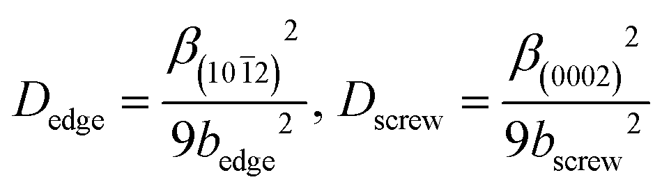
To investigate the crystal quality of the as-grown GaN films, high-resolution XRD measurements were carried out. Fig. 3 shows the symmetric (002) and asymmetric (102) XRD rocking curves (ω-scans) for both GaN samples. The full width at half-maximum (FWHM) values of the (002) diffraction peak for samples A and B are 318 and 284 arc sec respectively, and the FWHM values of the (102) diffraction peak for samples A and B are 464 and 325 arc sec respectively. The difference of (002) plane FWHM between the two samples is insignificant, while the (102) plane FWHM of sample A has a remarkable broadening about 140 arc sec compared with that of sample B. Since the FWHM of (002) and (102) rocking curves are related to the screw-type and edge-type TDs density respectively,25 the edge-type TDs density (Dedge) and screw-type TDs density (Dscrew) in the epitaxial layers can be estimated using the formulas:26
![[2 with combining macron]](https://www.rsc.org/images/entities/char_0032_0304.gif) 0].27
0].27
 | ||
| Fig. 3 Symmetric and asymmetric XRD rocking curves for both samples. (a) ω scans from (002) and (102) reflections for sample A; (b) ω scans from (002) and (102) reflections for sample B. | ||
To identify the residual stress of the two samples, the micro-Raman spectrum measurements with the E2 (h) phonon peak were carried out. The 417 cm−1 phonon peak of sapphire was used as a reference. As shown in Fig. 4, the principal E2 (h) peaks for sample A and sample B situated at 570.0 cm−1 and 570.5 cm−1 respectively, indicating strong residual compressive stress in both samples since the E2 (h) has an intrinsic value of 567.5 cm−1 for stress-free GaN.28 However, there is an obvious redshift (0.5 cm−1) of the E2 (h) peak of sample A compared with that of sample B, strongly suggesting that strain relaxation occurred in sample A.
 | ||
| Fig. 4 Micro-Raman spectra of the as-grown samples A and B. | ||
The relationship between the residual stress, σ, and the shift of the phonon peak, Δω, is derived as follows:29

Hence, the relaxed compressive stress in sample A can be calculated to be 0.20 GPa. In addition, the voids induced by InGaN interlayer (shown in Fig. 1(b)) may also contribute to the strain relaxation. Furthermore, the small amplitude of the A1(TO) and E1(TO) peaks are visible at 527 and 561 cm−1 respectively for sample A and only E1(TO) for sample B. The appearance of these peaks may be correlated with GaN islands formed in the initial growth stage and this is the subject of further investigation.30
Screw-type TDs are considered as the primary culprit in reverse-bias leakage current and are undesirable in electronic devices, therefore this method to obtain HR-GaN enjoys an advantage in control the leakage current paths for HEMTs devices, thus superior to typical approaches by decreasing the pressure or intentionally doping.
To study the electrical properties of the as-grown GaN films, Hall-effect measurements were carried out. The normally UID GaN, i.e., sample B, exhibits n-type conduction with sheet resistivity of 1.3 × 10³ Ω per square. However, sample A, i.e., the HR-GaN, exhibits high resistive character with a sheet resistivity of 2.1 × 10⁸ Ω per square which was five orders of magnitude higher than that of sample B. However, the carrier concentration was exactly on the contrary. The carrier concentration of sample A and sample B are 1.0 × 1012 cm−3 and 4.7 × 1016 cm−3, respectively. In addition, the Hall mobility of sample A is 112 cm2 V−1 s−1, which is nearly half of that of sample B (245 cm2 V−1 s−1). The mobility seems to show disagreement to the classical behavior that the mobility is increasing monotonically with the carrier concentration decreasing. However, this behavior can be well accounted for by the dislocation scattering model according to Weimann et al.31 and Ng et al.32 In the dislocation scattering model, the room temperature electron mobility as a function of net carrier concentration follows a family of bell-shaped curves. In the low carrier concentration regime (<5 × 1017 cm−3), the electron mobility is dominated by scattering at charged dislocation lines and increases monotonically with carrier concentration, while at higher carrier concentrations the limitation stems from scattering at ionized impurities and the electron mobility decreases monotonically with carrier concentration.32 With respect to samples A and B, both have a carrier concentration below 5 × 1017 cm−3 and the edge-type dislocations density of sample A is doubled as that of sample B. In this scenario, the dislocations may play a dominant role in determining the mobility of sample A and decrease the mobility even with lower carrier concentration. Since the pronounced decrease of carrier concentration and concomitantly significant increase in the resistivity, some compensation mechanism involving the impurities and structure defects could exist behind this phenomenon.
SIMS and TEM characterization help to provide insight into the electrical properties of the as-grown GaN films observed in Hall-effects results, due to the fact that the electrical properties of GaN are closely related to impurities and micro-structural defects. Fig. 5 shows the depth profile of C, H, O and In concentrations for sample A. The UID carbon (C) concentration increased one order of magnitude by introducing an InGaN interlayer, from 4.7 × 1016 cm−3 to 5.0 × 1017 cm−3. The segregation peak in the In profile indicates the relative depth of InGaN layer and inhomogeneity of In distribution. The In profile is much broader for the sample than designed InGaN thickness in Fig. 1(a), which can be correlated to the thermal induced In-diffusion process during the growth of HR-GaN layer.33 Unexpectedly, the hydrogen (H) and O concentrations vary in consistent with the fluctuation of In fraction within the InGaN layer. In general, UID carbon impurities originate from the metalorganics in MOCVD, and act as acceptors when substitute for N (CN).34 Oxygen can be leached from the quartz liner and has been demonstrated to act as donors (substituting for N, i.e., ON) in GaN,35 and atomic H is mainly produced by NH3 dissociation but plays a small role in n-GaN.36 Considering that the Si donors and Zn or Mg acceptors are not intentionally introduced in the growth chamber, C and O are believed to be the primary background impurity acceptor and donor in our HR-GaN films in this study respectively. Accordingly, it is probably that the impurity compensation from CN acceptors and the major donors such as ON and VN, as the most possible candidates involved in the HR compensation mechanism in this work.
 | ||
| Fig. 5 SIMS depth profiles of C, H, O and In concentrations for sample A of the top 1.1 μm thickness. | ||
TDs have been associated with charged centres in GaN films, and play an important role in determining the electrical properties of the films. Elsner et al. have calculated the electronic structure of screw and edge TDs in GaN and suggested that the stress fields surrounding the edge TDs are sufficiently large to trap intrinsic defects and impurities such as Ga vacancy (VGa), O and VGa–O complexes.37 Wickenden et al.18 have also presented that carbon impurity segregated primarily at the edge-type TDs for growth pressure >100 Torr, resulting in compensating acceptor states. Combining the XRD results and analysis above, it is reasonable to believe that the increase of carbon incorporation is probably induced by the increased edge-type TDs.
In order to further verify the increase of edge-type TDs in HR-GaN layer, representative cross-sectional TEM images for sample-A using two-beam diffraction conditions were performed, as shown in Fig. 6. A significant increase in TDs density after growth of the InGaN interlayer can be observed in Fig. 6(a). From the Burgers vector analysis using invisibility criteria,38 the TDs in Fig. 6(b) and (c) are determined to be almost pure edge TDs (marked with “e”) and mixed TDs (marked with “m”), and no pure screw TD can be found in marked area. Edge-type misfit dislocation (marked with “MD”) can also be found near the InGaN layer. Quantitative analysis on the cross-sectional image [Fig. 6(a)] leads to a total TDs density of ∼1.3 × 109 cm−2, which is consistent with the XRD results (0.6 × 109 cm−2). Therefore, the increased edge-type TDs may be responsible for the increasing C incorporation, thus causing the background compensation and contributing to the high resistivity. Further studies are currently underway to determine the influence of the thickness and In mole fraction of InGaN interlayer on the film resistivity.
 | ||
| Fig. 6 Cross-sectional TEM images of sample-A showing a variety of dislocations: (a) bright-field image of a region near the HR-GaN layer. White arrow highlights the degraded InGaN position. (b) Dark-field image of the marked area with g1 = [0002]. (c) Dark-field image of the marked area with g2 = [110]. | ||
Conclusions
In summary, UID HR-GaN film by introducing an annealed InGaN interlayer without decreasing the growth pressure was demonstrated. The as-grown UID GaN shows high resistivity, high Hall mobility, dramatically low carrier concentrations as well as good crystalline quality. It is found that the increased carbon incorporation induced by edge-type TDs which are caused by the InGaN interlayer is probably responsible for the high resistive character. This method could be an attractive choice to obtain HR-GaN buffer with better reproducibility and overcome drawbacks such as undesirable memory effects and large leakage current paths.Acknowledgements
This work was supported by National Natural Science Foundation of China (No. 61223005, 61376046, 11405017, 61574026), the Fundamental Research Funds for the Central Universities (No. DUT15LK15, DUT15RC(3)016, No. DUT16LK29), Liaoning Provincial Natural Science Foundation of China (No. 2014020004) and Jiangxi Provincial Natural Science Foundation of China (No. 20133ACB20005). The Open Fund of the State Key Laboratory on Integrated Optoelectronics (No. IOSKL2015KF18, No. IOSKL2015KF22).Notes and references
- M. Asif Khan, A. Bhattarai, J. N. Kuznia and D. T. Olson, Appl. Phys. Lett., 1993, 63, 1214 CrossRef.
- U. K. Mishra, P. Parikh and Y. F. Wu, Proc. IEEE, 2002, 90, 1022 CrossRef CAS.
- H. Huang, Y. C. Liang, G. S. Samudra and C. L. L. Ngo, IEEE Electron Device Lett., 2014, 35, 569 CrossRef CAS.
- H. Yu, D. Caliskan and E. Ozbay, J. Appl. Phys., 2006, 100, 033501 CrossRef.
- I. B. Rowena, S. L. Selvaraj and T. Egawa, IEEE Electron Device Lett., 2011, 32, 1534 CrossRef CAS.
- T. Mattila and R. M. Nieminen, Phys. Rev. B, 1997, 55, 9571 CrossRef CAS.
- S. Strite and H. Morkoç, J. Vac. Sci. Technol., B: Microelectron. Process. Phenom., 1992, 10, 1237 Search PubMed.
- J. W. P. Hsu, M. J. Manfra, R. J. Molnar, B. Heying and J. S. Speck, Appl. Phys. Lett., 2002, 81, 79 CrossRef CAS.
- B. S. Simpkins, E. T. Yu, P. Waltereit and J. S. Speck, J. Appl. Phys., 2003, 94, 1448 CrossRef CAS.
- B. Kim, D. Moon, K. Joo, S. Oh, Y. K. Lee, Y. Park, Y. Nanishi and E. Yoon, Appl. Phys. Lett., 2014, 104, 102101 CrossRef.
- S. Heikman, S. Keller, S. P. DenBaars and U. K. Mishra, Appl. Phys. Lett., 2002, 81, 439 CrossRef CAS.
- M. Silvestri, M. J. Uren and M. Kuball, Appl. Phys. Lett., 2013, 102, 073501 CrossRef.
- J. B. Webb, H. Tang, S. Rolfe and J. Bardwell, Appl. Phys. Lett., 1999, 75, 953 CrossRef CAS.
- D. S. Green, J. Appl. Phys., 2004, 95, 8456 CrossRef CAS.
- A. E. Wickenden, D. D. Koleske, R. L. Henry, R. J. Gorman, M. E. Twigg, M. Fatemi, J. A. Freitas and W. J. Moore, J. Electron. Mater., 2000, 29, 21 CrossRef CAS.
- J. Selvaraj, S. L. Selvaraj and T. Egawa, Jpn. J. Appl. Phys., 2009, 48, 121002 CrossRef.
- X. G. He, D. G. Zhao, D. S. Jiang, Z. S. Liu, P. Chen, L. C. Le, J. Yang, X. J. Li, S. M. Zhang, J. J. Zhu, H. Wang and H. Yang, Thin Solid Films, 2014, 564, 135 CrossRef CAS.
- A. E. Wickenden, D. D. Koleske, R. L. Henry, M. E. Twigg and M. Fatemi, J. Cryst. Growth, 2004, 260, 54 CrossRef CAS.
- D. D. Koleske, A. E. Wickenden, R. L. Henry and M. E. Twigg, J. Cryst. Growth, 2002, 242, 55 CrossRef CAS.
- M. E. Twigg, D. D. Koleske, A. E. Wickenden, R. L. Henry and S. C. Binari, Appl. Phys. Lett., 2001, 79, 4322 CrossRef CAS.
- S. M. Hubbard, G. Zhao, D. Pavlidis, W. Sutton and E. Cho, J. Cryst. Growth, 2005, 284, 297 CrossRef CAS.
- Y. Zhao, F. Wu, C.-Y. Huang, Y. Kawaguchi, S. Tanaka, K. Fujito, J. S. Speck, S. P. DenBaars and S. Nakamura, Appl. Phys. Lett., 2013, 102, 091905 CrossRef.
- A. B. Yankovich, A. V. Kvit, X. Li, F. Zhang, V. Avrutin, H. Y. Liu, N. Izyumskaya, Ü. Özgür, H. Morkoç and P. M. Voyles, J. Appl. Phys., 2012, 111, 023517 CrossRef.
- B. V. Daele, G. V. Tendeloo, K. Jacobs, I. Moerman and M. R. Leys, Appl. Phys. Lett., 2004, 85, 4379 CrossRef.
- B. Heying, X. H. Wu, S. Keller, Y. Li, D. Kapolnek, B. P. Keller, S. P. DenBaars and J. S. Speck, Appl. Phys. Lett., 1996, 68, 643 CrossRef CAS.
- E. Arslan, M. K. Ozturk, H. Cakmak, P. Demirel, S. Özçelik and E. Ozbay, J. Mater. Sci.: Mater. Electron., 2013, 24, 4471 CrossRef CAS.
- R. Liu, J. Mei, S. Srinivasan, H. Omiya, F. A. Ponce, D. Cherns, Y. Narukawa and T. Mukai, Jpn. J. Appl. Phys., 2006, 45, L549 CrossRef CAS.
- S. Tripathy, S. Chua, P. Chen and Z. Miao, J. Appl. Phys., 2002, 92, 3503 CrossRef CAS.
- D. Zhao, S. Xu, M. Xie, S. Tong and H. Yang, Appl. Phys. Lett., 2003, 83, 677 CrossRef CAS.
- M. Pophristic, F. Long, M. Schurman, J. Ramer and I. Ferguson, Appl. Phys. Lett., 1999, 74, 3519 CrossRef CAS.
- N. G. Weimann, L. F. Eastman, D. Doppalapudi, H. M. Ng and T. D. Moustakas, J. Appl. Phys., 1998, 83, 3656 CrossRef CAS.
- H. M. Ng, D. Doppalapudi, T. D. Moustakas, N. G. Weimann and L. F. Eastman, Appl. Phys. Lett., 1998, 73, 821 CrossRef CAS.
- D. Queren, M. Schillgalies, A. Avramescu, G. Brüderl, A. Laubsch, S. Lutgen and U. Strauß, J. Cryst. Growth, 2009, 311, 2933 CrossRef CAS.
- J. L. Lyons, A. Janotti and C. G. Van de Walle, Appl. Phys. Lett., 2010, 97, 152108 CrossRef.
- C. G. Van de Walle and J. Neugebauer, J. Appl. Phys., 2004, 95, 3851 CrossRef CAS.
- V. Garbe, B. Abendroth, H. Stoecker, A. Gavrilov, D. Cohen-Elias, S. Mehari, D. Ritter and D. C. Meyer, Cryst. Res. Technol., 2015, 50, 425 CrossRef CAS.
- J. Elsner, R. Jones, P. K. Sitch, V. D. Porezag, M. Elstner, T. Frauenheim, M. I. Heggie, S. Öberg and P. R. Briddon, Phys. Rev. Lett., 1997, 79, 3672 CrossRef CAS.
- T. Y. Wang, S. L. Ou, R. H. Horng and D. S. Wuu, CrystEngComm, 2014, 16, 5724 RSC.
Footnote |
| † Electronic supplementary information (ESI) available. See DOI: 10.1039/c6ra10696j |
| This journal is © The Royal Society of Chemistry 2016 |