
 Open Access Article
 This Open Access Article is licensed under a
 Creative Commons Attribution 3.0 Unported Licence
Low variability of single-molecule conductance assisted by bulky metal–molecule contacts†
Rubén R.
Ferradás
ab,
Santiago
Marqués-González
cd,
Henrry M.
Osorio
efg,
Jaime
Ferrer
ab,
Pilar
Cea
ef,
David C.
Milan
h,
Andrea
Vezzoli
h,
Simon J.
Higgins
h,
Richard J.
Nichols
h,
Paul J.
Low
*c,
Víctor M.
García-Suárez
*ab and
Santiago
Martín
*ei
aNanomaterials and Nanotechnology Research Center, University of Oviedo & CSIC, 33007 Oviedo, Spain. E-mail: vm.garcia@cinn.es
bDepartamento de Física, Universidad de Oviedo, 33007 Oviedo, Spain
cSchool of Chemistry and Biochemistry, University of Western Australia, 6009, Australia. E-mail: paul.low@uwa.edu.au
dDepartment of Chemistry, Graduate School of Science and Engineering, Tokyo Institute of Technology, Tokyo 152-8511, Japan
eDepartamento de Química Física, Facultad de Ciencias, Universidad de Zaragoza, 50009 Zaragoza, Spain. E-mail: smartins@unizar.es
fInstituto de Nanociencia de Aragón (INA) and Laboratorio de Microscopias Avanzadas (LMA), Edificio i+d. Campus Rio Ebro, Universidad de Zaragoza, C/Mariano Esquillor, s/n, 50017 Zaragoza, Spain
gDepartamento de Física, Escuela Politécnica Nacional, Av. Ladrón de Guevara, E11- 253, 170525 Quito, Ecuador
hDepartment of Chemistry, University of Liverpool, Liverpool, L69 7ZD, UK
iInstituto de Ciencia de Materiales de Aragón (ICMA), Universidad de Zaragoza-CSIC, 50009 Zaragoza, Spain
First published on 4th August 2016
Abstract
A detailed study of the trimethylsilylethynyl moiety, –C![[triple bond, length as m-dash]](https://www.rsc.org/images/entities/char_e002.gif) CSiMe3 (TMSE), as an anchoring group in metal|molecule|metal junctions, using a combination of experiment and density functional theory is presented. It is shown that the TMSE anchoring group provides improved control over the molecule–substrate arrangement within metal|molecule|metal junctions, with the steric bulk of the methyl groups limiting the number of highly transmissive binding sites at the electrode surface, resulting in a single sharp peak in the conductance histograms recorded by both the in situ break junction and I(s) STM techniques. As a consequence of the low accessibility of the TMSE group to surface binding configurations of measurable conductance, only about 10% of gold break junction formation cycles result in the clear formation of molecular junctions in the experimental histograms. The DFT-computed transmission characteristics of junctions formed from the TMSE-contacted oligo(phenylene)ethynylene (OPE)-based molecules described here are dominated by tunneling effects through the highest-occupied molecular orbitals (HOMOs). This gives rise to similar conductance characteristics in these TMSE-contacted systems as found in low conductance-type junctions based on comparably structured OPE-derivatives with amine-contacts that also conduct through HOMO-based channels.
CSiMe3 (TMSE), as an anchoring group in metal|molecule|metal junctions, using a combination of experiment and density functional theory is presented. It is shown that the TMSE anchoring group provides improved control over the molecule–substrate arrangement within metal|molecule|metal junctions, with the steric bulk of the methyl groups limiting the number of highly transmissive binding sites at the electrode surface, resulting in a single sharp peak in the conductance histograms recorded by both the in situ break junction and I(s) STM techniques. As a consequence of the low accessibility of the TMSE group to surface binding configurations of measurable conductance, only about 10% of gold break junction formation cycles result in the clear formation of molecular junctions in the experimental histograms. The DFT-computed transmission characteristics of junctions formed from the TMSE-contacted oligo(phenylene)ethynylene (OPE)-based molecules described here are dominated by tunneling effects through the highest-occupied molecular orbitals (HOMOs). This gives rise to similar conductance characteristics in these TMSE-contacted systems as found in low conductance-type junctions based on comparably structured OPE-derivatives with amine-contacts that also conduct through HOMO-based channels.
Introduction
Interest and progress in single-molecule electronics has surged over recent years as advances in synthetic chemistry, scanning probe microscopy and nanofabricated test platforms have made single molecule measurements not only possible, but relatively routinely available, whilst advances in quantum chemical codes and computing power permit more detailed analysis and modelling of results. However, the large variability in the conductance profiles of individual junctions1–8 necessitates not only substantial effort to obtain statistically significant datasets but also gives rise to more than one discrete value of the conductance of any given molecule-contacting group-electrode combination. These variations arise not only from the simplest conceptual models of how the molecule is physically or chemically bonded to the electrode surface,9 but also because even ‘atomically flat’ electrode surfaces feature a variety of arrangements of atoms, including atomic reconstructions in the presence of strongly binding molecules and inherent defects.For example, both for α,ω-alkanedithiols1–3,10 and for conjugated molecule bridges containing thiol (or thiolate) anchoring groups,4 rather than a unique value for the single molecule conductance in metal molecule junctions, three (or more11) single molecule conductance values are evident. These have been termed (albeit arbitrarily) low (L) or A-type; medium (M) or B-type; and high (H) or C-type conductance groups. These conductance groups have been attributed to differing contact morphologies between the contacting groups and the gold electrode(s).1,3,10 Multiple single molecule conductance values for metal|molecule|metal junctions have also been reported for other molecular systems contacted through a variety of other functional groups.5,6 In the case of the three conductance groups attributed to α,ω-alkanedithiols contacting gold, the higher conductance (M and H) groups show predominance on stepped or rough surfaces, whereas the lower conductance (L) groups are more evident on flat surface regions.3 Consistent with the notion that increased surface roughness promotes formation of higher-conductance junctions, in general, the higher conductance groups are more easily observed in the in situ STM break junction (STM-BJ) technique.12 In contrast, the lower conductance contact groups are more readily apparent in measurements carried out with the I(s) method, which does not entail direct substrate–tip contact prior to formation of the molecular junction.13 In addition, in measurements based on the use of a scanning probe microscope tip as one of the electrodes, such as the I(s) or the in situ STM-BJ methods, it is possible for the junction to be formed through contact of the tip with parts of the molecule other than the designated terminal contacting moiety,14,15 which opens new conductance paths and therefore further increases the range of conductance signatures offered by a single molecule. These issues of multiple and variable binding sites give justification for identifying surface anchoring groups which offer a simplified behaviour.
Of the various demonstrated and potential binding groups to be explored, trimethylsilylethynyl (TMSE), –CCSiMe3, has begun to emerge as an interesting candidate for molecule–gold contacts. Fichou and colleagues have demonstrated that 13-(trimethylsilyl)-1-tridecene-6,12-diyne and related long-chain aliphatic tailed trimethylsilylethynyl derivatives form well-ordered self-assembled monolayers (SAMs) on Au(111) substrates. Whereas SAMs of n-alkanethiols on Au(111) display numerous grain boundaries arising from various metastable Au–S structures, the trimethylsilylethynyl-derived films were shown to be homogeneous over areas of several hundreds of nm2, indicating a commensurability between the silyl-derived SAM and the underlying gold atoms comprising the surface.16,17 Furthermore, the observation of pit-etching suggests a strong Au–Si interaction in these SAM structures, rather than simple physisorption.16,18 These observations led to a proposal concerning the nature of the molecule–gold interaction in which electron-donation from the gold surface atoms to the silicon centre results in formation of a local surface complex featuring a five-coordinate, trigonal bipyramidal silicon; this process would be facilitated by the compact and electron-withdrawing alkynyl moiety.16–18 However, more recent studies have alluded to the critical role that dispersion forces play in the stability of these well-ordered monolayers,19 making extrapolation from the molecular environments and surface contacts in well-ordered self-assembled films to single-molecule junctions difficult.
The potential for the trimethylsilylethynyl moiety to serve as a contact group in single molecule electronics was perhaps first recognized by Aso et al.20 in a synthetic study, and by Millar et al.21 with initial STM break junction investigations demonstrating the formation of junctions with a TMSE terminated molecular wire, 1,4-bis(trimethylsilylethynyl)benzene, and Au contacts. The use of TMSE as a contacting group was later further established through conductance measurements on thin films and in single-molecule junctions of similar molecules.22,23 Related concepts using various silanes24 and the use of trimethylsilyl as a protecting group during the in situ fabrication of Au–C contacts25,26 are also deserving of note. Silacycles have also been demonstrated as contacting groups in single molecule junctions with Au contacts.27 However, one important feature of the molecular junctions Au|Me3SiCC–…–…–CCSiMe3|Au is the observation of a single, well resolved peak in the conductance histograms, which is in contrast to the multiple signatures or very broad histograms more commonly observed with conventional contacting groups.23 Theoretical studies of molecules with the trimethylsilylethynyl moiety contacted to gold electrodes have been also carried out.28 Using a semi-phenomenological model based on kinetic theory of charge transmission29 the authors found a rather good agreement between theory and experiment with just three adjustable parameters (the transmission gap ΔE+j and the width parameters Γ(L)j and Γ(R)j), and a limited interaction between the molecular orbitals and the substrate.
We now report single molecule conductance studies of a small series of amine- and trimethylsilylethynyl-contacted 1,4-bis(phenylethynyl)benzene molecules (Chart 1) which allow us to draw an unambiguous correlation between the contacting groups and the number of observed conductance peaks, supported by DFT calculations and first-principles transport simulations to better understand the nature and electrical properties of the –CCSiMe3|Au contact.
 | ||
| Chart 1 Compounds featured in this work. | ||
Experimental and theoretical methods
Synthetic work
The compounds 1,302,313![[thin space (1/6-em)]](https://www.rsc.org/images/entities/char_2009.gif) 32 and 520 were prepared by the literature procedures or minor variations; the synthesis of 4 and 6 are given in the ESI.†
32 and 520 were prepared by the literature procedures or minor variations; the synthesis of 4 and 6 are given in the ESI.†
Conductance measurements
Molecular adsorption was achieved by immersion of the gold-on-glass substrate in 0.5 mM THF solutions of the candidate molecule for about 40 s. The relatively short immersion times and low concentrations are aimed at promoting low coverage on the gold slide which in turn favours single molecule events. After adsorption, the sample was washed in ethanol and then dried in a stream of nitrogen. Both the in situ STM-BJ and the I(s) methods have been used to determine molecular conductance profiles of the target molecules (see ESI† for details). For a given set-point current and bias voltage, typically 5000–6000 events were observed. In this study all I(s) and in situ STM-BJ measurements were conducted in air. Traces with current plateaus below 1G0 in the current-versus-distance STM tip retraction events are synonymous with molecular junction formation,12,13 and these were selected from the majority of events in which no clear junctions evolve. This data selection avoids the ambiguity of including curves in which molecular junction formation does not occur. The selection is achieved by using the rational criterion of selecting traces with a current plateau which exceeds 0.1 nm in length. The traces selected using this criterion were then analyzed statistically in the form of histogram plots to determine the single molecule conductance. This need for data selection arises from the relatively low probability of forming molecular junctions (“hit rate” or junction formation probability33) with the TMSE contacts when compared with other more conventional anchoring groups deployed in single molecule electronics (see ESI† for more details). This low probability of forming junctions with TMSE contacts (here, ca. 450 traces with plateaus per 5000–6000 curves) is consistent with the earlier observations of Millar et al.21 for Me3SiCC–C6H4–CCSiMe3 in STM break junction experiments, which showed considerably fewer counts than analogues with other termini such as CCAu{P(OMe)3}.
Raman spectroscopy
Raman and surface-enhanced Raman scattering (SERS) spectra were collected using a Confocal Raman Imaging from Witec, model Alpha300M+ with an excitation wavelength of 633 nm. The power on the sample was ∼0.5 mW. Silver islands (thickness 9.1 nm) were prepared in an Edwards model 306 vacuum coater from a resistively heated tungsten boat. The substrates were Zuzi glass microscope slides cleaned in piranha solution for 30 min (3:1 97% H2SO4:30% H2O2), rinsed with deionized water, and dried in a stream of N2. Care: piranha solutions are exceptionally corrosive and highly oxidizing. Contact between piranha solutions and organic materials is considered extremely hazardous and must be avoided. During silver deposition, the background pressure was maintained at 5 × 10⁻⁷ Torr, and the deposition rate (0.02 nm3 s−1) was monitored on an Electron Beam Evaporator Auto 500 from BOC Edwards. After metal deposition, the modified substrates were annealed at 200 °C for 60 minutes. Samples were prepared by immersing the resulting silver-mirrored substrate in a 1 mM solution of 6 in hexane for 24 h.
Theoretical methods
Density functional theory (DFT) based calculations,34 as implemented in the SIESTA code,35 and quantum transport theory, as implemented in the SMEAGOL36 and GOLLUM37 codes were performed to elucidate the junction geometries, together with their electronic and transport properties. Further details are given in the ESI.†DFT computations of molecular conductance usually involve generation of transmission curves for a single relaxed molecular junction configuration. However, the numerical values of the computed conductance can have a strong dependence on fine details of the junction geometry, such as the nitrogen–gold or silicon–gold distances for example, which vary as the molecular dynamics (MD) simulations proceed. A different approach was therefore pursued here. To simulate the range of different molecular configurations that comprise the range of junctions formed in the experimental measurements, four different initial junction configurations were explored using ab initio molecular dynamics at room temperature for each of the compounds 1–3 (Chart 1 and Fig. 1).
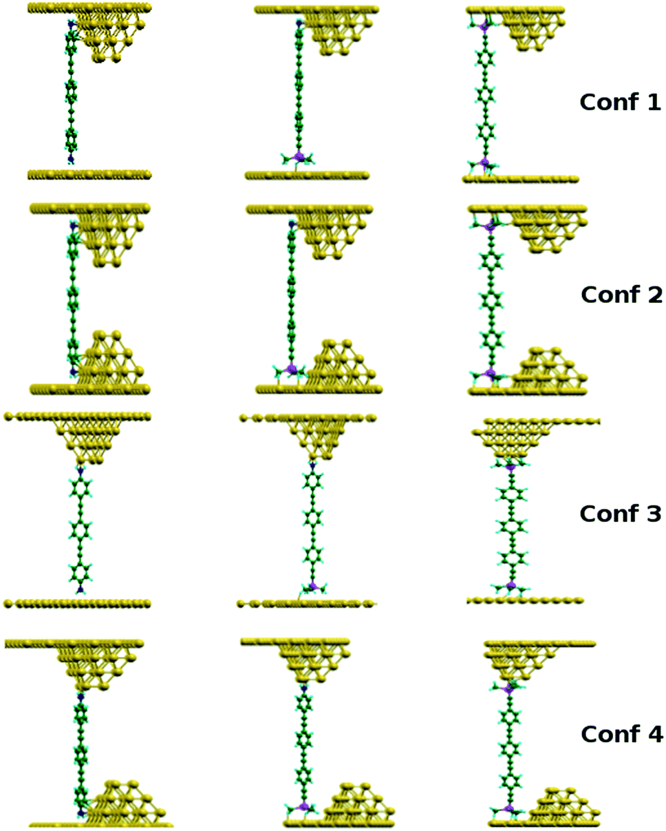 | ||
| Fig. 1 The four configurations (Conf. X, X = 1, 2, 3 and 4) used to start the ab initio molecular dynamics (MD) simulations of each junction for compounds 1, 2 and 3 (left, middle and right columns, respectively). | ||
In each case, a pyramid-shaped array of gold atoms and gold slab was employed as the top part of the junction, as a representative model of the STM tip. A flat Au(111) surface was used in the simulations to represent the bottom (substrate) electrode (cf.Fig. 1, Conf. 1 and Conf. 3). To account for molecules bonding at steps or rougher areas of the gold substrate surface, model junctions in which a gold pyramid is incorporated into the bottom electrode were also explored (cf.Fig. 1, Conf. 2 and Conf. 4). The molecules can bind to the pyramid either on top of it (Conf. 1 and Conf. 2) or sideways (Conf. 3 and Conf. 4). We excluded configurations where the molecule is initially on top of the pyramid on both sides because such arrangements are rather unstable (the molecule tends to move towards one of the surfaces) and do not give meaningful conductance values. These junction configurations lead to different chemical bonding arrangements for each of the three compounds through the two different contact groups (–NH2 and/or –CCSiMe3).
From these starting configurations, the positions of gold atoms within the gold pyramids and in the vicinity of the molecule, as well as the atoms in the molecule were allowed to move freely at each MD step. However, the positions of the gold atoms within the flat surfaces were fixed. Conductance histograms were built from the resulting evolved molecular junctions by calculating the conductance after every 10 MD steps. By computing over a relatively large number of MD generated configurations and generating theoretical conductance histograms junction-to-junction variations can be included in the computational result for better comparison to experiment.
Results and discussions
Single-molecule conductance
The oligo(phenylene)ethynylene (OPE) structure has been identified as an efficient “wire-like” molecular backbone and derivatives of various lengths featuring a wide variety of surface contacting groups have been studied in detail.4,38–43 The short chain oligomers 1, 2 and 3 (Chart 1) featuring different combinations of amine (–NH2) and trimethylsilylethynyl (TMSE), –CCSiMe3, contacting groups were prepared and studied in single molecule junctions by using both the in situ STM-BJ technique and I(s) method. As noted above, the rough or fractal nature of the cleaved gold contacts that comprise these STM-BJ junctions generally leads to the observation of higher conductance values (H and M groups), arising from the greater probability of binding molecules at under-coordinated sites on the electrode surfaces. In contrast, the I(s) method, which avoids a direct-metal–metal contact prior to the formation of the molecular junction, gives a greater proportion of L-group junctions. On this basis, the STM-BJ method was used to observe the higher conductance configurations (H and M groups) potentially offered by compounds 1–3, while the I(s) method was used to evaluate the lowest conductance junctions (L group). The single molecule conductance histograms for compounds 1–3 are summarized in Table 1.
The conductance profile of the bis(amine) substituted compound 1 shows two conductance values when the STM-BJ method was used, Fig. 2a (left). The conductance peak labelled as M (see also Table 1) is similar to the conductance value reported by Lu et al.38 for the same compound (101.0 ± 7.0 MΩ; ca. 12.8 × 10⁻⁵G0). Although the conductance peak labelled as H in Fig. 2a (left) has not been previously reported for 1, the observation of two conductance features in the histogram is consistent with the two conductance peaks reported for α,ω-diaminoalkanes from similar STM-BJ experiments.2 Lower conductance features (as the L-type) are difficult to observe with the in situ STM-BJ method. However, a detailed analysis closer to the noise level of the current amplifier in the STM-BJ scans of conductance–distance traces showed an L conductance peak at ca. 2.5 × 10⁻⁵G0 for 1 (Fig. S2a in the ESI†). To verify this observation, complementary measurements using the I(s) technique were also carried out. These measurements more clearly revealed the lowest conductance feature (L, Fig. 2a, right). This L-type conductance feature compares with the lowest conductance peak obtained for a closely-related thiol-contacted OPE-based molecule (2.0 × 10⁻⁵G0).4,39,44
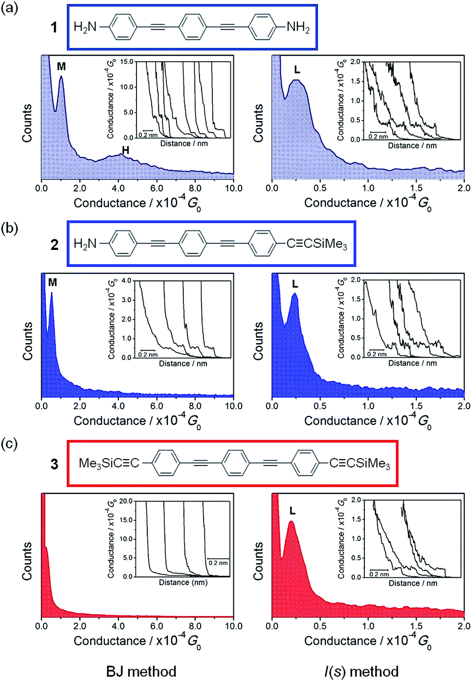 | ||
| Fig. 2 Conductance histograms built from summation of conductance traces (ca. 450) that showed discernible plateaus (with a current plateau which exceeds 0.1 nm in length) such as those displayed in the inset of the figures using either the STM-BJ technique (left side) or the I(s) method (right side). (a) Compound 1, (b) compound 2 and (c) compound 3. Conductance data are referenced to the conductance quantum G0 = 2e2/h = 77.5 μS. Utip = 0.6 V. | ||
For compound 2, which features both amine and trimethylsilylethynyl (TMSE) anchoring groups, a conductance peak was clearly observed (labelled as M in Fig. 2b, left) by the STM-BJ technique. Meanwhile a distinct lower value conductance peak (L) was obtained by both close analysis of the STM-BJ data (Fig. S2b†) and more clearly by the I(s) method (Fig. 2b, right). Comparison of these conductance data from 1 and 2 reveals three noteworthy points: (i) the similarity in the conductance value of the L group obtained for 1 and 2; (ii) the decrease in conductance of the M group in 2 compared to that in 1 and (iii) the absence of the H group for 2.
In the case of 3, bearing two TMSE contacts, current plateaus were difficult to observe in the STM-BJ data (Fig. 2c, left panel), although plateaus corresponding to a conductance of ca. 2.4 × 10⁻⁵G0 could be extracted from careful analysis of data near the limits of the amplifier (see Fig. S2c in ESI†). Nevertheless, this peak is in good agreement with the value obtained from the better-resolved data given by I(s) method (labelled as L in Fig. 2c, right panel). No data in the I(s) scans corresponding to another set of pronounced conductance plateaus (longer than 0.1 nm) could be detected below this marked L group. The similar conductance of the L groups for 1, 2 and 3 (Table 1) indicates that the configurations of the TMSE contact that give rise to the conductance peak with this group give electronic transmissions at the Au contact broadly similar to those of the low conductance-type amine (–NH2) contact, and reinforces the potential for TMSE to serve as an anchoring group in metal|molecule|metal junctions.22,23 The lower conductance of the M group in 2 when compared with 1 and the absence of the H group in 2 and 3 is consistent with the concept that the steric bulk of the SiMe3 moiety prevents the formation of high conductance features from binding at surface defect sites, which are apparent for anchoring groups such as –NH2, thiol1,2 or pyridyl.5
While it is conceivable that a diarylalkyne unit, such as those common to compounds 1–6 in this work, could interact with gold atom(s) via ‘side-on’ binding of the alkyne π-system,45 we can rule this out as a route to junction formation in this series because compound 5 did not give any evidence of junction formation in I(s) experiments.
The formation of highly transmissive Au–C contacts from addition of a nucleophile, such as tetrabutylammonium fluoride (TBAF), to TMS-terminated oligo(phenylene)ethynylenes25,26 to cleave in situ the trimethylsilyl (TMS) group or from addition of Me3Sn–alkyl bonds to gold surfaces46,47 as well as, more recently, the spontaneous formation of Au–C contacts with terminal alkynes,48 might suggest that for 2 and 3 the TMS group attached to the alkynyl could be also cleaved in situ and, therefore, to form Au–C contacts. To explore this possibility, a study of the stability of the terminal TMS moiety in the presence of Au was carried out by attempting to synthesize TMSE-capped gold nanoparticles (AuNPs), details of which are given in the ESI.† When trimethylsilylethynylbenzene (Me3SiCCC6H5) was investigated as a AuNP capping ligand, it did not perform well as an AuNP phase-transfer reagent, either in hexane or in benzene. In contrast, when phenylacetylene (HCCC6H5) was used as capping ligand, a complete phase transfer in both solvents was observed. These results are strongly suggestive of the retention of the SiMe3 in the presence of Au.
To further probe the surface binding properties of the –CCSiMe3 group, quartz crystal microbalance (QCM) experiments were carried out. A high surface coverage of 7.32 × 10⁻¹⁰ mol cm−2 was obtained for 3 (see ESI† for more details). In sharp contrast, when the –CCSiMe3 groups were replaced by triisopropylsilylethynyl (–CCSiPri3) groups (4, Chart 1) or by a 1,1-dimethyl-but-3-yne (tert-butylethynyl, –CCCMe3) fragment (5, Chart 1) no frequency change (Δf) for a QCM quartz resonator before and after incubation in a solution of these compounds was observed. Thus, while the TMSE group binds to the gold surface,16,17 when the methyl groups in TMSE are replaced by bulkier isopropyl groups or the silicon atom by carbon, the molecule–surface interaction is dramatically diminished. Furthermore, single-molecule conductance studies of 4 and 5 using both the STM-BJ and the I(s) methods failed to reveal current traces with the plateaus associated with the formation of molecular bridges (plateaus longer than 0.1 nm).
Finally, to demonstrate the retention of the TMS group, Raman and SERS studies of TMSE have also been carried out. Fig. 3 shows the Raman spectra of the model compound 6, which bears only a single TMSE contacting group, in the solid state as a powder as well as the SERS spectrum of a pristine self-assembled monolayer (SAM) of 6 deposited on silver mirrors. Both spectra show three major vibrational bands at 2210 (ν(CC)), 1597 (ν(C![[double bond, length as m-dash]](https://www.rsc.org/images/entities/char_e001.gif) C)aryl), and 1131 (ν(C–H)aryl) cm−1 that indicate that 6 remains intact after being assembled on the silver substrate. Nevertheless and the most important point, the presence of the TMS vibration band at 1452 cm−1 in the SAM of 6 (shifted by 48 cm−1 with respect to the powder, Fig. 3), and the absence of any new band at ∼400 cm−1 characteristic of a metal–C stretching mode (with metal being Au, Ag, or Pd)49 confirms the retention of the SiMe3 group and the lack of any formation of metal–C σ-bonds by the cleavage of the TMS group.25,26,49
C)aryl), and 1131 (ν(C–H)aryl) cm−1 that indicate that 6 remains intact after being assembled on the silver substrate. Nevertheless and the most important point, the presence of the TMS vibration band at 1452 cm−1 in the SAM of 6 (shifted by 48 cm−1 with respect to the powder, Fig. 3), and the absence of any new band at ∼400 cm−1 characteristic of a metal–C stretching mode (with metal being Au, Ag, or Pd)49 confirms the retention of the SiMe3 group and the lack of any formation of metal–C σ-bonds by the cleavage of the TMS group.25,26,49
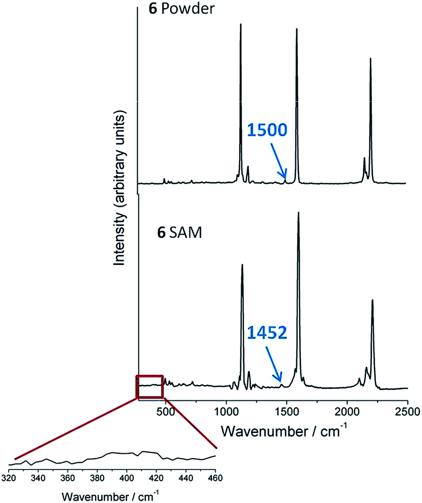 | ||
| Fig. 3 Raman spectra of 6 in the solid state and as a self-assembled monolayer on a silver mirror. | ||
Together, all these observations underline the essential role of the Si atom and the balance of steric effects near the contact for fabricating transmissive metal–molecule–metal junctions. An analysis of the average lengths of the current plateaus also supports the selective binding of the TMSE moiety to specific sites on the electrodes; see ESI.†
To further explore the contact geometry of the TMSE moiety and the gold electrodes, and to better understand the electrical characteristics of these junctions, attention was turned to DFT computations and modeling studies.
DFT calculations
Room-temperature molecular dynamics (MD) simulations of the variety of junction configurations shown in Fig. 1 were carried out. The anchoring groups at the top of the figures were initially placed contacting either the base or the apex of the gold pyramid simulating the tip. The TMSE groups were allowed to slide down to the base of a pyramid to which they bind during the MD runs. Anchor groups at the gold substrate contacted either at a flat terrace region, or close to a pyramid base, and were then allowed to evolve during the MD runs.The room-temperature MD simulations indicate that compound 1 binds most often to a top, a hollow or a bridge gold site on the terrace regions of the substrate electrode via the –NH2 group. In a small number of cases the junction conformation evolved to situations where the molecule binds to the substrate pyramid via a π-type interaction with the associated phenyl ring, or through both the –NH2 and the phenyl ring at the same time.5,15,50,51 Similar amine binding motifs are found for the top electrode contact for compound 1. Similar junction behaviour was also observed for the top –NH2 electrode of compound 2.
The TMSE groups in 2 and 3 bind to the gold atoms at the substrate (bottom) electrode in different ways. At a terrace, the TMSE group binds weakly via the methyl groups to the surface. There is no significant re-arrangement of the local silicon geometry with C–Si–C bond angles ranging from 89–115°, and Si–CC bond lengths of 1.22–1.26 Å (CC) and 1.71–1.95 Å (Si–C). The tetrahedral geometry at silicon and positioning of the methyl groups in contact with the surface results in the silicon atom being displaced more than 3.5 Å from the surface, and thereby interacting only weakly with the Au surface atoms.
To assess the stability of the junctions, as well as to obtain a first insight into the nature of the interaction between the gold surface and the TMSE group, the binding energies for surface configurations where the TMSE group of compound 3 molecules lie in the hollow, top and bridge positions of a flat gold surface have been computed. Interestingly, binding energies around and above 0.5 eV are found, and simple estimates based on the Arrhenius law suggest long stability times. These binding energies are compiled in Table 2, where the hollow site is shown to be about 150 meV more stable than the top or bridge configurations. In simulations where the surface features a pyramid (Fig. 1, Conf. 2 and Conf. 4) the binding energies are further increased by about 150 meV, suggesting that compound 3 will preferably place itself at irregularities of the surface such as steps rather than in the middle of the terraces.52 The suggested reduced phase space for molecule positioning is consistent with the lower hit rates found in our experiments.
CSiMe3 group of compound 3 for different positions and configurations. The surface + pyramid configuration corresponds to cases that model the L-conductance group. The group is considered as either binding to a “terrace surface” at either hollow, top or bridge sites, or at a mixed “surface + pyramid” contact (e.g. as illustrated in Fig. 1, right column, Conf. 1, top contact)
| Configuration | Hollow | Top | Bridge |
|---|---|---|---|
| Terrace surface | 0.59 eV | 0.40 eV | 0.45 eV |
| Surface + pyramid | 0.74 eV | 0.61 eV | 0.53 eV |
These findings are in excellent agreement with the data obtained by Fichou et al. from SAMs of TMSE functionalised unsaturated hydrocarbons on flat gold substrates.28,29 The Fichou group report SAMs exhibit excellent registry with the underlying gold surface, consistent with the positioning of the TMSE group at the hollow sites. The higher binding energy calculated here is consistent with the stability of the films and the significant binding energy is consistent with the evidence of pit-etching. However, in contrast to the initial proposals of a local five-coordinate silicon complex, the calculations here indicate a subtler molecule–substrate interaction.
To understand better the nature of the molecule–surface interaction, the charge redistribution upon binding has been estimated using a Mulliken population analysis. Whilst the silicon atom retains its four coordinate tetrahedral configuration, there is a charge transfer from the substrate to the molecule, which varies during the MD steps between 0.4–0.8 electrons. Most of the transferred charge is placed at the methyl groups and is distributed equally among them. In contrast, the central silicon atoms only gain ∼0.1 electrons each. This charge transfer to the molecule and its associated image charge at the surface are likely responsible for the shifts in Si 2p and Au 4f7/2 core levels observed by Fichou's team in SR-PES experiments with TMSE based SAMs on gold.16–18
A significant junction conductance (see below) with compound 3 is only achieved if the molecule binds to a pyramid as depicted in Conf. 2 of Fig. 1. A closer inspection of the junction geometry reveals that the methyl groups of the TMSE fragment must be oriented as shown in Fig. 4a in order to give rise to junctions with appreciable conductance signatures. Here, the –CCSiMe3 group interacts with gold atoms in the flat surface at the base of the pyramid and with gold atoms in the pyramid. In this configuration the silicon atom is placed as close as possible to the pyramid and minimizes the Si⋯Au separation. Importantly, the estimated charge transfer from the surface towards the molecule is largest in this junction geometry, rising to as much as 0.8–0.9 electrons. This configuration corresponds to the maximum binding energy shown in Table 2; hence in this configuration charge transfer, binding energy and conductance are maximized. Furthermore, this enhanced charge transfer increases the ionic character of the molecule–surface interaction. Further examination of the junction geometries indicates that the bulky nature of the SiMe3 group prevents the interaction of the phenyl ring π-system with gold atoms at the pyramid and close interactions of the phenyl rings in the molecular backbone and the gold atoms of the defect site models are not found in the MD simulations.
 | ||
| Fig. 4 A top view of the relative –CCSiMe3 group-pyramid arrangements. Blue, green, magenta and yellow atoms represent hydrogen, carbon, silicon and gold atoms, respectively. Only the gold atoms of the pyramid are shown but not the underlying gold terrace. | ||
Another arrangement found in many MD steps is depicted in Fig. 4b. Here, in contrast to the more conductive geometry shown in Fig. 4a, the methyl groups prevent a closer approach of the silicon atoms to the pyramid. As a result, charge transfer towards the molecule is reduced to 0.5 electrons with concomitant decreases in the binding energy and the conductance. Indeed, these configurations do not produce a conductance peak in the theoretically-generated histograms (see below).
In summary, in contrast to the multiple strongly binding junction geometries identified for NH2 contacts, the bonding between the TMSE group and flat terrace surfaces and single atom defects is relatively weak, and largely van der Waals in nature. On the other hand, the TMSE group can bind more strongly to the pyramid-decorated model surface, with a significant degree of charge transfer (∼0.8 to 0.9 electrons gained per molecule) leading to the stronger interactions, and a stabilization of the junction through the resulting image charge. Thus, when the TMSE group is directed in such a way to allow the closest approach of the Si atom to the Au pyramid, a significant binding energy is achieved and junction conductance corresponding to the L-conductance group is obtained. The ionic character and image charge stabilization plays an important role in the stability and conductance profiles of these structures. The steric bulk of the methyl groups prevents the close approach of the silicon atom and gold surface, and the resulting charge-separated structures hold some analogy with molecular frustrated Lewis pairs.53
The conductance histograms for molecular junctions of 1, 2 and 3 derived from the MD simulations are shown in Fig. 5. An outline of the procedure is as follows: each MD run commences using one of the initial junction configurations shown in Fig. 1. These configurations are allowed to evolve during the MD simulation, which run typically for 300 steps of 1 fs. The conductance is computed every 10 MD steps. The conductance values for a given compound are compiled in the histograms shown in Fig. 5. Note that each of the peaks contains contributions from several atomic arrangements, which are classified according to their gross similarity to the initial snapshots shown in Fig. 1. A breakdown of these contributions is summarized in Table 3. As an example, configurations 1 and 3 in Fig. 1 contribute 60% and 40% respectively, to the low conductance peak found for compound 1. The statistics of the simulation data is limited by the computational cost of the simulations and are not as large as those obtained experimentally. In spite of the smaller statistical datasets these histograms feature several peaks which correspond to the conductance groups in the experimental conductance histograms, as discussed below.
 | ||
| Fig. 5 Conductance histograms of (a) compound 1, (b) compound 2 and (c) compound 3. Vertical dashed lines correspond to the experimental values of the conductance groups (e.g. three conductance groups for 1, two conductance groups for 2 and one conductance group for 3). | ||
| L-group | M-group | H-group | |
|---|---|---|---|
| 1 | Conf. 1 (∼60%) | Conf. 1 (∼20%) | Conf. 1 (∼33%) |
| Conf. 2 (∼20%) | Conf. 2 (∼42%) | ||
| Conf. 3 (∼40%) | Conf. 3 (∼30%) | Conf. 3 (∼8%) | |
| Conf. 4 (∼30%) | Conf. 4 (∼17%) | ||
| 2 | Conf. 1 (∼27%) | Conf. 1 (∼55%) | |
| Conf. 2 (∼21%) | Conf. 2 (∼42%) | ||
| Conf. 3 (∼44%) | |||
| Conf. 4 (∼8%) | Conf. 4 (∼3%) | ||
| 3 | Conf. 1 (∼21%) | ||
| Conf. 2 (∼70%) | |||
| Conf. 3 (∼9%) |
The number of conductance peaks featuring in the calculated histograms agrees with the experimental results for each of the three compounds: three, two and one conductance peaks for compounds 1, 2 and 3, respectively (Table 3). The poorer statistics results in a third conductance peak for 1 in Fig. 5a being under-developed, although a number of configurations give conductance values which cluster close to the experimental H group value. It should also be noted that for the computational data represented in Fig. 5 there is an uncertainty in the choice of bin size which is most suited for generating the histogram, as discussed further in the ESI.† Nevertheless, the theoretical and experimental position of the conductance peaks agrees quantitatively for 1 (Fig. 5a).
The two conductance peaks shown in Fig. 5b for compound 2 are slightly shifted towards smaller values with respect to the experimental peaks, indicated by the broken vertical lines. This may be due to a slightly incorrect placement of the Fermi level with respect to the molecular HOMO and LUMO energies. For compound 3, only those junctions in which the TMSE group adopts the special position shown in Fig. 4a contribute to the single conductance peak show in Fig. 5c. Any other configuration yields conductance values below 10−7 to 10−8G0. The larger disagreement between the experimental value and the computationally-generated conductance peak for 3 is due to the rather small values produced from the simulated junction configuration. However, the further reduced phase space of configurations yielding measurable conductance values is consistent with the lower hit rates found experimentally for compound 3.
To verify the robustness of the calculated conductance histograms and verify the statistics that lead to the appearance of a conductance peak, junctions of compound 3 with a shorter distance between the surfaces have also been studied. In such compressed junction configurations the molecular backbone distorts and compresses but the molecule remains perpendicular to the surface and a similar, but better resolved, conductance peak develops at a similar conductance value in the computational histogram.
In order to gain further understanding on the mechanisms that give rise to each conductance group, the transmission coefficient T(E) as a function of energy E corresponding to a representative data point in each group (L, M, H) was examined (Fig. 6). The low-voltage conductance of the junction is estimated as T(EF), where EF is the Fermi energy. The Fermi level appears roughly in the middle of the molecular HOMO–LUMO gap in all cases, which means that the junctions fall in the tunneling regime. Notice there is an uncertainty in the exact position of the Fermi level, as DFT does not give this position accurately, which can explain the smaller values of the transmission of compound 3 compared to the other two compounds. In these transmission curves, peaks at negative energies to the left of the gap correspond to HOMO resonances, while peaks on the right of the gap, at positive energy values, correspond to LUMO resonances.
 | ||
| Fig. 6 Transmission as a function of energy for a junction comprising (a) compound 1, (b) compound 2 and (c) compound 3 on a gold surface with pyramids. | ||
In the case of 1, the enhancement of the conductance from the L to the M and H groups is due to an increase of the transmission in the gap, which in turn originates from a slight increase of the width of the HOMO resonance, while the energy position of the HOMO level itself remains relatively constant. These width changes come from changes in the hybridization between the –NH2 group and the surface gold atoms. Note that, according to the local density of states (LDOS), the HOMO in all these molecules is spread roughly through the whole molecule and is affected by the interaction with the electrodes, in contrast to earlier assumptions.28
In the transmission curve for 3 (Fig. 6c), the arrangement shown in Fig. 4a corresponds to the L group observed in the experimental measurements. Although this is labeled a ‘low’ contact configuration in the analysis of experimental results, the conductance of this junction is higher than other cases observed in the MD simulations of this compound. The higher relative conductance for this arrangement versus other junction geometries comes from a competition between two factors. The first is that the resonance width increases from 5 meV to 8 meV, which enhances the conductance of the junction and can be traced back to a larger molecular orbital–electrode hybridization. In contrast, the second is a shift of the HOMO transmission resonance to lower (more negative) energies, which serves to decrease the junction conductance. On balance, the shift in the HOMO resonance cannot compensate for the increased molecule–surface interactions, and as a result the conductance increases.
Transmission curves for junctions formed from compounds 4 (with triisopropylsilylethynyl, –CCSiPri3, anchor groups) and 5 (with tert-butylethynyl, –CCCMe3, anchor groups) were also calculated. Fig. 7 compares the transmission of triisopropylsilylethynyl contacted 4 and trimethylsilylethynyl contacted 3 on a flat surface and demonstrates the conductance is much smaller for 4. This further confirms that the use of the very bulky isopropyl groups leads to very low or no observable conductance. Various configurations for compound 5 starting from seeds similar to those that gave the L group for 3 were also explored. Although the transmission curves from 5 resembled those of 3, the conductance at the Fermi level was 2–3 times smaller. This low conductance and lack of surface binding apparent from the QCM studies indicates that the tert-butylethynyl group is unlikely to produce junctions with a significant conductance in agreement with the experimental observation.
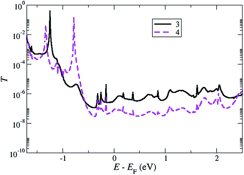 | ||
| Fig. 7 Transmission as a function of energy for a junction comprising 3 and 4 (solid black and magenta dashed solid lines, respectively) on a flat gold surface (without pyramids), calculated at the equilibrium distances (3.8 Å and 5.0 Å from the Si atom to the surface for 3 and 4, respectively). | ||
Conclusions
We have shown here that the trimethylsilylethynyl moiety, –CCSiMe3, provides a means to control the range of conductive molecule–metal contacts within molecular junctions. Thus, whilst the TMSE molecules can form weak van der Waals-type contacts with some ionic character on terraces at top, bridge and hollow sites, the conductance of these configurations is lower than the detection limits of the experiments. Rather, in stark contrast to the initial models derived from extrapolation of binding in well-ordered self-assembled films, contacts at defect sites within a very narrow range of molecular orientations are necessary to allow an increase of the binding energy between the TMSE group and the gold atoms. This enhanced interaction serves to stabilize the binding of the molecule to the surface through overlaps and an image charge or electrostatic model. The net effect on the molecular conductance comes from the hybridization between the molecular levels and the gold atoms, which increases the width of the resonances (from 5 meV to 8 meV) and overall enhances the transmission at the Fermi level.
The very specific molecular orientation necessary for achieving significant molecular conductance results in a single low-conductance peak for the TMSE-terminated compound 3, which contrasts to the multiple conductance features of the amine-terminated compound 1. This special binding geometry also results in low probabilities for junction formation in in situ STM BJ experiments as well as I(s) measurements, which makes it necessary to apply data selection when constructing conductance histograms with this contacting group. Nevertheless, the single conductance feature observed with –CCSiMe3 termini is similar to conductance values from the L-type contacts on gold substrates with amine (–NH2) anchor groups. In summary, the –CCSiMe3 group is a promising contact for use in fundamental studies of molecular junctions in cases where a single, well-defined conductance histogram is required, although the resulting molecular conductance is likely to be low.
Acknowledgements
R. R. F. thanks the Consejería de Educación del Principado de Asturias for a Severo Ochoa grant (BP11-069). V. M. G.-S. thanks the Spanish Ministerio de Economía y Competitividad for a Ramón y Cajal fellowship (RYC-2010-06053). R. R. F., J. F. and V. M. G.-S. wish to acknowledge financial support from the Spanish grant FIS2012-34858 and the Marie Curie Network MOLESCO. They also wish to acknowledge the supercomputing facility CESGA where part of the calculations was carried out. P. C. and S. M. are grateful for financial assistance from the Ministerio de Economía y Competitividad of Spain in the framework of the project CTQ2012-33198 as well as the award of the CTQ2013-50187-EXP grant. H. M. O., P. C., and S. M. thank the support from DGA and Fondos FEDER for funding through the Platon research group. H. M. O. is also grateful for financial assistance from the Secretaría Nacional de Educación Superior, Ciencia, Tecnología e Innovación from Ministerio de Educación (Ecuador). S. M. thanks the Ministerio de Educación from Spain for financial support through the framework of the Campus de Excelencia Internacional, CEI Iberus. S. J. H., R. J. N., P. J. L. and S. M.-G. thank the EPSRC for funding (EPSRC grants EP/K007785/1, EP/H035184/1, EP/K007548/1, EP/H005595/1). P. J. L. holds an Australian Research Council Future Fellowship (FT120100073) and gratefully acknowledges funding for this work from the ARC (DP140100855). The authors also thank I. Echaniz for technical support in Raman studies, and J. B. G. Gluyas for the synthesis of 6.References
- C. Li, I. Pobelov, T. Wandlowski, A. Bagrets, A. Arnold and F. Evers, J. Am. Chem. Soc., 2008, 130, 318–326 CrossRef CAS PubMed.
- F. Chen, X. L. Li, J. Hihath, Z. F. Huang and N. J. Tao, J. Am. Chem. Soc., 2006, 128, 15874–15881 CrossRef CAS PubMed.
- W. Haiss, S. Martin, E. Leary, H. van Zalinge, S. J. Higgins, L. Bouffier and R. J. Nichols, J. Phys. Chem. C, 2009, 113, 5823–5833 CAS.
- N. Weibel, A. Blaszczyk, C. von Haenisch, M. Mayor, I. Pobelov, T. Wandlowski, F. Chen and N. J. Tao, Eur. J. Org. Chem., 2008, 136–149 CrossRef CAS.
- C. S. Wang, A. S. Batsanov, M. R. Bryce, S. Martin, R. J. Nichols, S. J. Higgins, V. M. Garcia-Suarez and C. J. Lambert, J. Am. Chem. Soc., 2009, 131, 15647–15654 CrossRef CAS PubMed.
- S. Martin, W. Haiss, S. J. Higgins and R. J. Nichols, Nano Lett., 2010, 10, 2019–2023 CrossRef CAS PubMed.
- M. Kamenetska, S. Y. Quek, A. C. Whalley, M. L. Steigerwald, H. J. Choi, S. G. Louie, C. Nuckolls, M. S. Hybertsen, J. B. Neaton and L. Venkataraman, J. Am. Chem. Soc., 2010, 132, 6817–6821 CrossRef CAS PubMed.
- S. Y. Quek, M. Kamenetska, M. L. Steigerwald, H. J. Choi, S. G. Louie, M. S. Hybertsen, J. B. Neaton and L. Venkataraman, Nat. Nanotechnol., 2009, 4, 230–234 CrossRef CAS PubMed.
- A. M. Bratkovsky and P. E. Kornilovitch, Phys. Rev. B: Condens. Matter Mater. Phys., 2003, 67, 115307 CrossRef.
- X. L. Li, J. He, J. Hihath, B. Q. Xu, S. M. Lindsay and N. J. Tao, J. Am. Chem. Soc., 2006, 128, 2135–2141 CrossRef CAS PubMed.
- J. F. Zhou, F. Chen and B. Q. Xu, J. Am. Chem. Soc., 2009, 131, 10439–10446 CrossRef CAS PubMed.
- B. Q. Xu and N. J. J. Tao, Science, 2003, 301, 1221–1223 CrossRef CAS PubMed.
- W. Haiss, H. van Zalinge, S. J. Higgins, D. Bethell, H. Hobenreich, D. J. Schiffrin and R. J. Nichols, J. Am. Chem. Soc., 2003, 125, 15294–15295 CrossRef CAS PubMed.
- J. S. Meisner, M. Kamenetska, M. Krikorian, M. L. Steigerwald, L. Venkataraman and C. Nuckolls, Nano Lett., 2011, 11, 1575–1579 CrossRef CAS PubMed.
- M. Kiguchi, O. Tal, S. Wohlthat, F. Pauly, M. Krieger, D. Djukic, J. C. Cuevas and J. M. van Ruitenbeek, Phys. Rev. Lett., 2008, 101, 046801 CrossRef CAS PubMed.
- A. Marchenko, N. Katsonis, D. Fichou, C. Aubert and M. Malacria, J. Am. Chem. Soc., 2002, 124, 9998–9999 CrossRef CAS PubMed.
- N. Katsonis, A. Marchenko, S. Taillemite, D. Fichou, G. Chouraqui, C. Aubert and M. Malacria, Chem.–Eur. J., 2003, 9, 2574–2581 CrossRef CAS PubMed.
- N. Katsonis, A. Marchenko, D. Fichou and N. Barrett, Surf. Sci., 2008, 602, 9–16 CrossRef CAS.
- A. Nion, N. Katsonis, A. Marchenko, C. Aubert and D. Fichou, New J. Chem., 2013, 37, 2261–2265 RSC.
- M. Endou, Y. Ie, T. Kaneda and Y. Aso, J. Org. Chem., 2007, 72, 2659–2661 CrossRef CAS PubMed.
- D. Millar, L. Venkataraman and L. H. Doerrer, J. Phys. Chem. C, 2007, 111, 17635–17639 CAS.
- G. Pera, S. Martin, L. M. Ballesteros, A. J. Hope, P. J. Low, R. J. Nichols and P. Cea, Chem.–Eur. J., 2010, 16, 13398–13405 CrossRef CAS PubMed.
- S. Marques-Gonzalez, D. S. Yufit, J. A. K. Howard, S. Martin, H. M. Osorio, V. M. Garcia-Suarez, R. J. Nichols, S. J. Higgins, P. Cea and P. J. Low, Dalton Trans., 2013, 42, 338–341 RSC.
- R. Emanuelsson, H. Lofas, J. Zhu, R. Ahuja, A. Grigoriev and H. Ottosson, J. Phys. Chem. C, 2014, 118, 5637–5649 CAS.
- W. J. Hong, H. Li, S. X. Liu, Y. C. Fu, J. F. Li, V. Kaliginedi, S. Decurtins and T. Wandlowski, J. Am. Chem. Soc., 2012, 134, 19425–19431 CrossRef CAS PubMed.
- Y. C. Fu, S. J. Chen, A. Kuzume, A. Rudnev, C. C. Huang, V. Kaliginedi, M. Baghernejad, W. J. Hong, T. Wandlowski, S. Decurtins and S. X. Liu, Nat. Commun., 2015, 6, 6403 CrossRef CAS PubMed.
- T. A. Su, J. R. Widawsky, H. X. Li, R. S. Klausen, J. L. Leighton, M. L. Steigerwald, L. Venkataraman and C. Nuckolls, J. Am. Chem. Soc., 2013, 135, 18331–18334 CrossRef CAS PubMed.
- E. G. Petrov, A. Marchenko, O. L. Kapitanchuk, N. Katsonis and D. Fichou, Mol. Cryst. Liq. Cryst., 2014, 589, 3–17 CrossRef CAS.
- E. G. Petrov, V. May and P. Hanggi, Chem. Phys., 2005, 319, 380–408 CrossRef CAS.
- A. J. Deeming, G. Hogarth, M. Y. V. Lee, M. Saha, S. P. Redmond, H. T. Phetmung and A. G. Orpen, Inorg. Chim. Acta, 2000, 309, 109–122 CrossRef CAS.
- Y. G. Zhi, S. W. Lai, Q. K. W. Chan, Y. C. Law, G. S. M. Tong and C. M. Che, Eur. J. Org. Chem., 2006, 14, 3125–3139 CrossRef.
- W. M. Khairul, L. Porres, D. Albesa-Jove, M. S. Senn, M. Jones, D. P. Lydon, J. A. K. Howard, A. Beeby, T. B. Marder and P. J. Low, J. Cluster Sci., 2006, 17, 65–85 CrossRef CAS.
- D. Z. Manrique, C. Huang, M. Baghernejad, Z. Zhao, O. A. Al-Owaedi, H. Sadeghi, V. Kaliginedi, W. Hong, M. Gulcur, T. Wandlowski, M. R. Bryce and C. J. Lambert, Nat. Commun., 2015, 6, 6389 CrossRef CAS PubMed.
- W. Kohn and L. J. Sham, Phys. Rev., 1965, 140, A1133 CrossRef.
- J. M. Soler, E. Artacho, J. D. Gale, A. Garcia, J. Junquera, P. Ordejon and D. Sanchez-Portal, J. Phys.: Condens. Matter, 2002, 14, 2745–2779 CrossRef CAS.
- A. R. Rocha, V. M. Garcia-Suarez, S. Bailey, C. Lambert, J. Ferrer and S. Sanvito, Phys. Rev. B: Condens. Matter Mater. Phys., 2006, 73, 085414 CrossRef.
- J. Ferrer, C. J. Lambert, V. M. Garcia-Suarez, D. Z. Manrique, D. Visontai, L. Oroszlany, R. Rodriguez-Ferradas, I. Grace, S. W. D. Bailey, K. Gillemot, H. Sadeghi and L. A. Algharagholy, New J. Phys., 2014, 16, 093029 CrossRef.
- Q. Lu, K. Liu, H. M. Zhang, Z. B. Du, X. H. Wang and F. S. Wang, ACS Nano, 2009, 3, 3861–3868 CrossRef CAS PubMed.
- S. Martin, I. Grace, M. R. Bryce, C. S. Wang, R. Jitchati, A. S. Batsanov, S. J. Higgins, C. J. Lambert and R. J. Nichols, J. Am. Chem. Soc., 2010, 132, 9157–9164 CrossRef CAS PubMed.
- R. Huber, M. T. Gonzalez, S. Wu, M. Langer, S. Grunder, V. Horhoiu, M. Mayor, M. R. Bryce, C. S. Wang, R. Jitchati, C. Schonenberger and M. Calame, J. Am. Chem. Soc., 2008, 130, 1080–1084 CrossRef CAS PubMed.
- S. M. Wu, M. T. Gonzalez, R. Huber, S. Grunder, M. Mayor, C. Schonenberger and M. Calame, Nat. Nanotechnol., 2008, 3, 569–574 CrossRef CAS PubMed.
- Z. Y. Ng, K. P. Loh, L. Q. Li, P. Ho, P. Bai and J. H. K. Yip, ACS Nano, 2009, 3, 2103–2114 CrossRef CAS PubMed.
- P. Moreno-Garcia, M. Gulcur, D. Z. Manrique, T. Pope, W. J. Hong, V. Kaliginedi, C. C. Huang, A. S. Batsanov, M. R. Bryce, C. Lambert and T. Wandlowski, J. Am. Chem. Soc., 2013, 135, 12228–12240 CrossRef CAS PubMed.
- W. Haiss, C. S. Wang, I. Grace, A. S. Batsanov, D. J. Schiffrin, S. J. Higgins, M. R. Bryce, C. J. Lambert and R. J. Nichols, Nat. Mater., 2006, 5, 995–1002 CrossRef CAS PubMed.
- M. Bochmann, Organometallics 2: Complexes with Transition Metal–Carbon π-Bonds, Oxford University Press, U.S.A, 1994 Search PubMed.
- Z. L. Cheng, R. Skouta, H. Vazquez, J. R. Widawsky, S. Schneebeli, W. Chen, M. S. Hybertsen, R. Breslow and L. Venkataraman, Nat. Nanotechnol., 2011, 6, 353–357 CrossRef CAS PubMed.
- W. B. Chen, J. R. Widawsky, H. Vazquez, S. T. Schneebeli, M. S. Hybertsen, R. Breslow and L. Venkataraman, J. Am. Chem. Soc., 2011, 133, 17160–17163 CrossRef CAS PubMed.
- P. Pla-Vilanova, A. C. Aragones, S. Ciampi, F. Sanz, N. Darwish and I. Diez-Perez, Nanotechnology, 2015, 26, 381001 CrossRef PubMed.
- L. Laurentius, S. R. Stoyanov, S. Gusarov, A. Kovalenko, R. B. Du, G. P. Lopinski and M. T. McDermott, ACS Nano, 2011, 5, 4219–4227 CrossRef CAS PubMed.
- L. Venkataraman, J. E. Klare, I. W. Tam, C. Nuckolls, M. S. Hybertsen and M. L. Steigerwald, Nano Lett., 2006, 6, 458–462 CrossRef CAS PubMed.
- Z. Li and D. S. Kosov, Phys. Rev. B: Condens. Matter Mater. Phys., 2007, 76, 035415 CrossRef.
- The computed binding energies for the NH2 group were similar and the relative stability order on the surface was the same (the hollow configuration was the most stable). Interestingly, the binding energies in the presence of the pyramid were comparable to those on the surface, excluding some configurations that gave rise to various conductance peaks, which were 0.1–0.2 eV higher. This indicates a lower tendency for this group to bind to defects on the surface. The binding energy was found however to be larger at undercoordinated gold atoms on the pyramids.53 Some of such configurations were also calculated and contributed to the conductance groups (see Fig. 1 and Table 3). Differences in values between our binding energies and those in previous studies54 can be attributed to the basis set (SZP + diffuse orbitals on the electrodes) and the exchange and correlation potential (LDA).
- D. W. Stephan, Org. Biomol. Chem., 2008, 6, 1535–1539 CAS.
- S. Y. Quek, L. Venkataraman, H. J. Choi, S. G. Louie, M. S. Hybertsen and J. B. Neaton, Nano Lett., 2007, 7, 3477–3482 CrossRef CAS PubMed.
Footnote |
| † Electronic supplementary information (ESI) available: Detail synthetic procedures; additional conductance data; stability of the terminal TMS moiety, QCM measurements, and details of the procedures used in the theoretical calculations. See DOI: 10.1039/c6ra15477h |
| This journal is © The Royal Society of Chemistry 2016 |