Self-organized ZnO nanorods prepared by anodization of zinc in NaOH electrolyte†
Junzhe Donga,
Zhuofeng Liub,
Junye Donga,
Dessy Ariyantia,
Zhenjiang Niuc,
Saifang Huanga,
Weijun Zhangb and
Wei Gao*a
aDepartment of Chemical & Materials Engineering, The University of Auckland, Auckland 1142, New Zealand. E-mail: w.gao@auckland.ac.nz
bCollege of Aerospace and Materials Engineering, National University of Defense Technology, Changsha 410073, China
cInstitute of Physical Chemistry, Zhejiang Normal University, Jinhua 321004, China
First published on 29th July 2016
Abstract
A new type of self-assembled zinc oxide (ZnO) nanostructure has been prepared by electrochemical anodization of zinc foil in NaOH aqueous electrolyte. Under optimized anodization conditions, well defined nanorods were obtained with a stacking nanoparticle layer on the top and straight cellular structures underneath. The relationships between the morphology of the nanostructures and anodization parameters were studied in detail through field-emission scanning electron microscopy (FESEM), X-ray powder diffraction (XRD) and energy-dispersive X-ray spectrometry (EDS). The experimental results indicate that the primary factor affecting the anodic nanostructure is the applied voltage, while anodization time and electrolyte concentration also play significant roles in tailoring the nanorod morphology.
1. Introduction
Due to the direct wide band gap (around 3.4 eV), large exciton binding energy (60 meV) and high electron mobility,1 zinc oxide (ZnO) has attracted great attention over past decades and found potential applications in light emission,2 photocatalysis,3 and optoelectronic and sensor devices.4,5 A wide range of ZnO nanostructures can be obtained through different techniques, such as hydrothermal processes,6 chemical vapour deposition (CVD)7 and template-directed methods.8 Apart from these methods, electrochemical anodization appears to be an efficient, highly controllable and cost effective approach to fabricate ZnO.9Unlike titanium and other valve metal that have been successfully anodized with regular nanoporous or nanotubular structure,10,11 amphoteric anodic ZnO is hard to form with similar ordered morphology due to its instability in both acidic and alkaline electrolytes. However, various ZnO nanostructures can be prepared through anodization.12–16 Nanosheet and nanoflower morphologies are usually present in acidic electrolytes anodization. While nanoparticle and nanowire shapes are prone to appear in alkaline solution. It is interesting that even nanoporous ZnO can be synthesized in DI water through anodization.17
Among different morphologies, highly ordered nanoporous and nanotubular oxide with large surface-volume ratio have wide potential applications.18–21 Therefore, much effort has been made to tailor anodic ZnO into tubular shape through changing experimental conditions, such as anodizing Zn foil in sulphides based electrolyte22 or at extreme low temperature.23 Recently, Ono et al.24 reported a method for fabricating anodic ZnO with porous structure in NaOH solution. However, little attention has been paid to the morphology evolution during anodization process.
In this paper we present a facile approach to produce anodic ZnO nanorods in NaOH electrolyte and report a progress in understanding formation mechanism and morphology control of this anodization system. At the beginning we prepared well-defined nanorods for the first time by electrochemical anodization and then studied mechanism of nanorods formation. We investigated the effect of experimental conditions on the morphology evolution and proposed optimization of reaction conditions. These results may provide information to design well-aligned one-dimensional ZnO nanostructures for various applications.
2. Experimental procedure
2.1. Preparation of anodic nanostructures
Cold-worked Zn foils (99.99% purity) of 0.2 mm thick were cut into specimens with size of 30 × 25 × 0.2 mm. Surface of foils were mechanically polished to mirror-like surface by 3 μm diamond suspension prior to anodization. Subsequently, they were ultrasonically cleaned successively in acetone, ethanol and distilled water, and placed in a nitrogen stream for drying. Zn foils were used as the anode in a two-electrode cell, while titanium mesh placed at a distance of 3 cm as the cathode. The anodization process was performed in NaOH aqueous electrolyte with constant stirring at ambient temperature. Different DC voltages (5–40 V), anodization time (0.5–1.5 h) and concentrations of NaOH electrolytes (0.05 M to 0.2 M) were employed. The resulted anodized foils were then cleaned in distilled water to remove remaining electrolyte and immersed in ethanol for 12 h at room temperature. Finally, they were dried and stored in a desiccator for characterization.2.2. Characterization of anodic nanostructures
The surface and cross-section morphologies of synthesized films were observed with a field-emission scanning electron microscopes (FESEM, Philips XL-30S) operating at 5 kV. Their crystal structures were studied through X-ray powder diffraction (XRD, D2-Phaser, Bruker, Germany) with Cu Kα1 radiation (λ = 1.5406 Å). XRD patterns were recorded at a 2θ range of 20 to 80°. The chemical composition was characterized using energy-dispersive X-ray spectrometer (EDS).3. Results and discussion
3.1. Formation of regular nanorods ZnO
The FESEM of anodic film is illustrated in Fig. 1a and b. From cross sectional view in Fig. 1a, anodic film is composed of a thin compacted layer on the surface and vertically ordered cellular structure underneath. The top view in Fig. 1b shows surface layer is densely arranged and piled up nanoparticles. XRD was employed to confirm crystal structure of synthesized film. As shown in Fig. 1c, the pronounced diffraction peaks with green diamonds can be indexed as ZnO although most obvious peaks marked by blue dots belong to the Zn substrate. These ZnO diffraction peaks correspond to (100), (002) and (101) lattice planes, indicating polycrystalline nature of anodic ZnO film. In addition, XRD patterns of the anodic films after annealing (Fig. S1†) only show the narrowing full width at half maximum (FWHM) of ZnO peaks, illustrating larger grain size and better crystallization with increasing annealing temperature. Normally the anodic film that has amorphous structure can be fabricated through electrochemical anodization 25–27or converted to crystalline phase with post annealing.28 The ZnO with hexagonal wurtzite structure fabricated directly by anodization without annealing can be attributed to unique regular cellular structure, which provides a path for ionic conduction and promote the growth of crystallized ZnO.29 The composition of anodic film was characterized through EDS, which also confirms the formation of ZnO.30 It can be seen in Fig. 1d that Zn and O account for the main elements and their atomic ratio is approximately 1. The elements composition of cross-sectional layer also refers to the ZnO nanostructure obtained (Fig. S2†).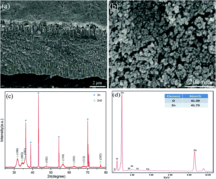 | ||
| Fig. 1 FESEM images of (a) cross-sections and (b) surface of anodic film prepared in 0.1 M NaOH aqueous electrolytes with 12 V for 1 h; (c) XRD patterns and (d) area scanning EDS spectrum of (b). | ||
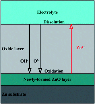
The formation of anodic ZnO film can be attributed to dynamic competition between Zn oxidation, chemical etching and field-assisted dissolution. Under certain anodization conditions, oxidation rate and dissolution rate will reach a dynamic equilibrium at a steady state and oxide layer with critical thickness can be obtained.31 As shown in Fig. 2, oxygen-containing anions, such as O2− and OH−, migrate to substrate/oxide interface to form oxide layers as following :32
| Zn + O2− → ZnO + 2e− | (1) |
| Zn + OH− → ZnO + H+ + 2e− | (2) |
Two dissolution processes simultaneously contribute to the final shape of anodic ZnO film. One is the chemical etching occurring on the top surface of oxide due to presence of H+ ions.33 The other is electrochemical etching happening in the oxide/electrolyte interface at bottom of oxide layer. Their relevant chemical reactions are as following:
| ZnO + 2H+ → Zn2+ + H2O | (3) |
| ZnO + OH− ↔ ZnOOH− | (4) |
As for the formation of nanoparticles on surface (Fig. 1b), it has a close relationship with the unevenly distributed partial corrosion.12 Newly formed ZnO layers should not be flat, resulting in inhomogeneous distribution of electric field. The amorphous oxides or convex parts tend to be etched preferentially with the help of chemical etching and anisotropic field-assisted dissolution following reactions (3) and (4), leading to partially dissolved ZnO nanoparticles.
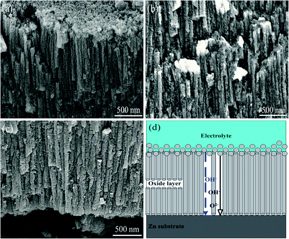
The detailed information about cellular morphology underneath is given in Fig. 3a–c. The upper, middle and bottom parts have smooth and straight cellular shape with similar width (∼80 nm). Formation of such kind of orderly nanostructure can be attributed to ions transportation under electric field as shown in Fig. 3d. During anodization process, thickness-varying electric field E is established through oxide layer under a constant voltage U. The generated E can enhance the oxidation rate as well as dissolution rate. According to Tafel's law,34 inward oxygen-containing ionic current j, which determines oxidation rate, has exponential relationship with E. Under effective electric field, transition of oxygen-containing anions to substrate/oxide interface will be promoted marked by dark arrow in Fig. 3d, leading to consecutive generation of ZnO following reactions (1) and (2). On the other hand, E can cause polarization and impairment of Zn–O bond, which facilitate the preferential dissolution effect of OH− following reaction (4) illustrated by blue arrow in Fig. 3d. Finally, a dynamic balance between oxidation and dissolution is reached, leading to the formation of well-defined cellular structure and relatively thick ZnO layer.
This nanostructure was further investigated from sectional views. As shown in Fig. 4, straight cellular arrays are closely packed and separate from each other marked by yellow dots from top section view. However, there are no pores inside the cellular structure from bottom section view, which is different from the nanotubes prepared by Ti anodization. Therefore, it can be assumed that the as-formed cell-like structures are nanorods rather than nanotubes.
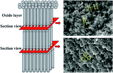 | ||
| Fig. 4 Section view of anodic film prepared for 1 h in 0.1 M NaOH aqueous electrolytes under 12 V. Yellow dots and circles outlines the shape of nanorods. | ||
3.2. Effect of anodization conditions on the nanostructure of ZnO
Generally, thick layers with rough structures can be obtained with high voltage, long duration time and high temperature.35 We investigated the effects of applied voltage, duration time and electrolyte concentration on the morphology evolution of anodic ZnO.Fig. 5a–c show the porous morphology obtained with 5, 7 and 9 V having an average thickness of ∼1.60 μm. When the applied voltage increases to 12 V, separate straight cells with thickness of 6–7 μm formed similar to Keller's model of porous alumina (Fig. 5d). The formation of nanoporous structure can be attributed to insufficient supply of U. E varies directly with U and inversely with oxide thickness d, which can be written as following :28
| E = U/d | (5) |
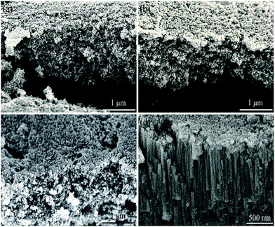 | ||
| Fig. 5 FESEM cross-section images of anodic films prepared in 0.1 M NaOH aqueous electrolytes for 1 h at various voltages of (a) 5 V, (b) 7 V, (c) 9 V, and (d) 12 V. | ||
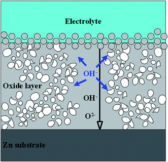
As thickness of oxide layer increases with reaction progress, strength of E weakens under constant U. When U is lower than 9 V, corresponding E is too weak to drive oxygen-containing ions through the oxide layers to form ZnO as marked by black line in Fig. 6 and oxidation process will eventually stop. Therefore, the thickness of whole layers prepared under different voltages stays constant around 1.6 μm. Due to migration rate of anions reducing with increase of d, residual OH− ions tend to diffuse freely and attack formed ZnO randomly as shown by blue arrow (Fig. 6), resulting in porous nanostructures. When U increases to 12 V, critical value of electric field Ec and oxide layer thickness dc will be constant at a steady state, resulting in unchanged oxidation and dissolution rate.36 Consequently, dynamic balance will be reached, leading to production of regular nanorod arrays.
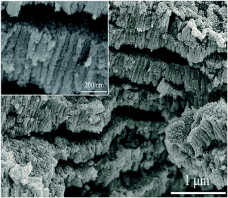
As the voltages increase to high values of 20, 30 and 40 V, ZnO layers become thicker (Fig. S3†). However, abnormal stacking and cracking take place on the cross-sectional area, as shown in Fig. 7. Nanorod arrays still locate perpendicularly to the substrates with gaps or cracks between layers. Inside the gaps, numerous nanoparticles appear similar to the granular surface. This phenomenon was also reported in the anodization of tin.37,38 The discontinuities of anodic layers can be attributed to the fast growth of layers and violent production of oxygen during anodization. As anodization process is accelerated under high voltages, oxygen is supposed to release rapidly. Vigorous oxygen evolution may disturb local stresses of oxide/substrate interface. Therefore, brittle nanorods arrays are apt to crack along horizontal direction, and long-range structural order is destroyed. As for the nanoparticles that are sandwiched between separate layers, their production derives from dissolution of synthesized nanorods through OH− etching. In addition, more gaps or cracks are present inside layers with increasing voltages (shown in Fig. S3†) due to larger amount of oxygen liberations.
4. Conclusions
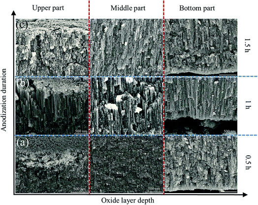
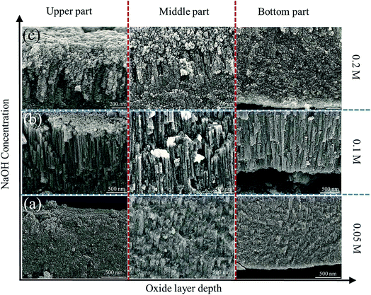
We have demonstrated a facile method to prepare a new type of self-assembled ZnO nanostructure. Well-aligned anodic ZnO nanorods have been fabricated by anodization Zn metal using the optimized conditions in 0.1 M NaOH aqueous electrolytes at 12 V for 1 h. The obtained ZnO layer is ∼7 μm thick and composed of nanorods of ∼80 nm width with compact granular morphology on the surface. Applied voltage plays a crucial role in determining the morphology of ZnO. While porous structures can be obtained at voltages below 12 V, nanorods ZnO layer are formed at high voltages. However, cracking inside the layers happened at voltages over 20 V due to oxygen evolution. Anodization time and electrolyte concentration make minor modification to the synthesized nanorods. Short time and low NaOH concentration give rise to bulk-like ZnO layer or poor rod-shape, while excessive time and high concentration produce over-etching nanorods.Acknowledgements
The authors would like to acknowledge the assistance offered by the staff in Department of Chemical and Materials Engineering at the University of Auckland, especially Ms Catherine Hobbis and Dr Alec Asadov. J Dong would also like to thank the China Scholarship Council (CSC) for the scholarship. The authors would like to thank financial support by Open Research Fund of Top Key Discipline of Chemistry in Zhejiang Provincial Colleges and Key Laboratory of the Ministry of Education for Advanced Catalysis (ZJHX201512).References
- L.-L. Yang, Q. Zhao, M. Willander, J. Yang and I. Ivanov, J. Appl. Phys., 2009, 105, 053503 CrossRef.
- Y.-C. Wang, I.-C. Leu and M.-H. Hon, J. Cryst. Growth, 2002, 237, 564–568 CrossRef.
- C. Tian, Q. Zhang, A. Wu, M. Jiang, Z. Liang, B. Jiang and H. Fu, Chem. Commun., 2012, 48, 2858–2860 RSC.
- X.-Y. Liu, C.-X. Shan, S.-P. Wang, H.-F. Zhao and D.-Z. Shen, Nanoscale, 2013, 5, 7746–7749 RSC.
- Y. Huang, Y. Zhang, Y. Gu, X. Bai, J. Qi, Q. Liao and J. Liu, J. Phys. Chem. C, 2007, 111, 9039–9043 CAS.
- J.-M. Jang, C.-R. Kim, H. Ryu, M. Razeghi and W.-G. Jung, J. Alloys Compd., 2008, 463, 503–510 CrossRef CAS.
- C. L. Wu, L. Chang, H. G. Chen, C. W. Lin, Y. C. Chao and J. K. Yan, Thin Solid Films, 2006, 498, 137–141 CrossRef CAS.
- H. J. Fan, W. Lee, R. Scholz, A. Dadgar, A. Krost, K. Nielsch and M. Zacharias, Nanotechnology, 2005, 16, 913 CrossRef CAS.
- S. Ono, Y. Kobayashi, R. Kobayashi and H. Asoh, ECS Trans., 2008, 16, 353–358 CAS.
- P. Roy, S. Berger and P. Schmuki, Angew. Chem., Int. Ed., 2011, 50, 2904–2939 CrossRef CAS PubMed.
- S. Z. Chu, K. Wada, S. Inoue, M. Isogai and A. Yasumori, Adv. Mater., 2005, 17, 2115–2119 CrossRef CAS.
- G. Huang, X. Wu, Y. Cheng, J. Shen, A. Huang and P. Chu, Appl. Phys. A: Mater. Sci. Process., 2007, 86, 463–467 CrossRef CAS.
- Z. Hu, Q. Chen, Z. Li, Y. Yu and L.-M. Peng, J. Phys. Chem. C, 2009, 114, 881–889 Search PubMed.
- J. Zhao, X. Wang, J. Liu, Y. Meng, X. Xu and C. Tang, Mater. Chem. Phys., 2011, 126, 555–559 CrossRef CAS.
- A. Ramirez-Canon, D. O. Miles, P. J. Cameron and D. Mattia, RSC Adv., 2013, 3, 25323–25330 RSC.
- S. Sreekantan, L. R. Gee and Z. Lockman, J. Alloys Compd., 2009, 476, 513–518 CrossRef CAS.
- A. Shetty and K. K. Nanda, Appl. Phys. A: Mater. Sci. Process., 2012, 109, 151–157 CrossRef CAS.
- E. Balaur, J. M. MacAk, L. Taveira and P. Schmuki, Electrochem. Commun., 2005, 7, 1066–1070 CrossRef CAS.
- R. Beranek, H. Tsuchiya, T. Sugishima, J. Macak, L. Taveira, S. Fujimoto, H. Kisch and P. Schmuki, Appl. Phys. Lett., 2005, 87, 243114 CrossRef.
- O. K. Varghese, D. Gong, M. Paulose, K. G. Ong, E. C. Dickey and C. A. Grimes, Adv. Mater., 2003, 15, 624–627 CrossRef CAS.
- H. Tsuchiya, J. M. Macak, L. Müller, J. Kunze, F. Müller, P. Greil, S. Virtanen and P. Schmuki, J. Biomed. Mater. Res., Part A, 2006, 77, 534–541 CrossRef PubMed.
- N. K. Shrestha, K. Lee, R. Hahn and P. Schmuki, Electrochem. Commun., 2013, 34, 9–13 CrossRef CAS.
- N. K. Shrestha, R. Hahn, K. Lee, A. Tighineanu and P. Schmuki, ECS Electrochem. Lett., 2014, 3, E1–E3 CrossRef CAS.
- S. Ono, Y. Kobayashi and H. Asoh, ECS Trans., 2008, 13, 183–189 CAS.
- D. Gong, C. A. Grimes, O. K. Varghese, W. Hu, R. Singh, Z. Chen and E. C. Dickey, J. Mater. Res., 2001, 16, 3331–3334 CrossRef CAS.
- A. W. Amer, S. M. Mohamed, A. M. Hafez, S. Y. AlQaradawi, A. S. Aljaber and N. K. Allam, RSC Adv., 2014, 4, 36336–36343 RSC.
- R. V. Gonçalves, P. Migowski, H. Wender, A. F. Feil, M. J. Zapata, S. Khan, F. Bernardi, G. M. Azevedo and S. R. Teixeira, CrystEngComm, 2014, 16, 797–804 RSC.
- O. K. Varghese, D. Gong, M. Paulose, C. A. Grimes and E. C. Dickey, J. Mater. Res., 2003, 18, 156–165 CrossRef CAS.
- X. Xiao, K. Ouyang, R. Liu and J. Liang, Appl. Surf. Sci., 2009, 255, 3659–3663 CrossRef CAS.
- V. Galstyan, E. Comini, C. Baratto, G. Faglia and G. Sberveglieri, Ceram. Int., 2015, 41, 14239–14244 CrossRef CAS.
- J. Dong, J. Han, W. Qiu, S. Huang and W. Gao, Scr. Mater., 2013, 69, 374–376 CrossRef CAS.
- S. Xu and Z. L. Wang, Nano Res., 2011, 4, 1013–1098 CrossRef CAS.
- S. J. Kim, J. Lee and J. Choi, Electrochim. Acta, 2008, 53, 7941–7945 CrossRef CAS.
- N. Cabrera and N. F. Mott, Rep. Prog. Phys., 1949, 12, 163 CAS.
- T. Torchynska and B. El Filali, J. Lumin., 2014, 149, 54–60 CrossRef CAS.
- Z. Su, G. Hähner and W. Zhou, J. Mater. Chem., 2008, 18, 5787–5795 RSC.
- H.-C. Shin, J. Dong and M. Liu, Adv. Mater., 2004, 16, 237–240 CrossRef CAS.
- A. Palacios-Padrós, M. Altomare, A. Tighineanu, R. Kirchgeorg, N. Shrestha, I. Diez-Perez, F. Caballero-Briones, F. Sanz and P. Schmuki, J. Mater. Chem. A, 2014, 2, 915–920 Search PubMed.
Footnote |
| † Electronic supplementary information (ESI) available: Description of XRD patterns, EDS spectra and FESEM images. See DOI: 10.1039/c6ra16995c |
| This journal is © The Royal Society of Chemistry 2016 |

