Role of multipolar plasmon resonances during surface-enhanced Raman spectroscopy on Au micro-patches†
Annette
Dowd
*a,
Mathias
Geisler
ab,
Shaoli
Zhu
a,
Michelle L.
Wood
a and
Michael B.
Cortie
 a
a
aSchool of Mathematical and Physical Sciences, University of Technology Sydney, PO Box 123, Broadway NSW 2007, Australia. E-mail: Annette.Dowd@uts.edu.au
bDepartment of Photonics Engineering, Technical University of Denmark, Oersteds Plads 343, 2800 Kgs. Lyngby, Denmark
First published on 7th December 2016
Abstract
The enhancement of a Raman signal by multipolar plasmon resonances – as opposed to the more common practice of using dipolar resonances – is investigated. A wide range of gold stars, triangles, circles and squares with multipolar resonances in the visible region were designed and then produced by electron beam lithography. We used 633 nm excitation and Rhodamine 6G as a probe molecule to confirm that, although the dipolar resonances of these shapes lie well into the infrared, SERS in the visible can still be obtained by coupling to their ‘dark mode’ multipolar resonances. However, the magnitude of enhancement in any given shape varied significantly and stochastically. Electromagnetic simulations were used to probe this surprising phenomenon further. These revealed that the presence or absence of a multipolar plasmon resonance at an particular excitation wavelength depended critically on the size and symmetry of the shape being examined, with a good SERS response only possible if the peak of the multipolar resonance is aligned with the 633 nm laser excitation.
Introduction
Surface enhanced Raman spectroscopy (SERS) has been shown to yield zeptomolar or even single molecule detection under suitable conditions.1–4 In general, amplification of the Raman signal relies upon the generation of strong, localized electric fields on a metallic substrate and, importantly, the positioning of the analyte molecules within such regions of high intensity.1,2,5–9 Typically, the enhanced electric field is generated by a localised surface plasmon resonance (LSPR). Electrochemically roughened silver surfaces are the original, canonical example of an enhancing substrate, although aggregates of colloidal particles of Ag or Au are now also commonly used.1,2,10 There is also some interest in investigating the use of arrays of specifically designed silver or gold nanoparticles for this purpose.6,8,9 This is so that the location, volume and intensity of the enhanced electric field on the substrate can be controlled, which is an essential requirement for reproducible SERS.2 Use of a defined nanostructure also offers the prospect of a means to calibrate the enhancement signal as otherwise the number of ‘hot spots’ producing the enhancement, the number of molecules contained within them, and the magnitude of the enhancement, are stochastic and unpredictable.2,5,8The production of suitable arrays using electron beam lithography (EBL) has been investigated by many groups and offers the advantages of repeatability, relative predictability of results, tunability of designs and reasonable spatial resolution (see ref. 1, 7–9 and 11–13 and citations within them). These advantages are offset to some extent by the very high cost of EBL (and other top-down techniques such as focused ion beam milling),2,8 and by the fact that the enhancements recorded from structures made by EBL are generally three or four orders of magnitude lower than those observed on colloidal aggregates.9 Nanosphere lithography (NLS) is an alternative and popular technique, for making SERS-active substrates1,8,14 but the technique is restricted to only a few designs of nanostructure such as triangles,14 hexagons,8 semi-shells of various kinds,15,16 or nano-crescents.17
Generally, the stated purpose for studying periodic arrays of shapes produced by EBL or NLS is to provide a controlled way to test the fundamental relationships between predicted or measured electromagnetic properties and enhancement.12 If high sensitivity is required for practical analyses then colloidal aggregates or roughened silver would probably still be the more popular choice in working laboratories.
The prevailing dogma in respect of lithographically-produced shapes is that sharp tips will lead to generation of electric field hotspots7,8,18 (the so-called lightning-rod effect19) and hence a greater enhancement of the Raman signal. It has been recognized, however, that in some geometries the enhancement could come from multipolar resonances along the flanks or upper surfaces of the shapes rather from their tips.9,13,18,20 In any event, the shape and size of the nanostructure is often chosen so that a LSPR wavelength, corresponding to an increase in far-field extinction, is similar to the Raman excitation laser wavelength6–9,14 However, this principle is not universally valid; for example, the best SERS enhancement offered by colloidal aggregates of noble metal nanoparticles or some other geometries is not well correlated with their far-field optical extinction spectra.5,8,9,21 In addition, nanoscale surface roughness, from thermal evaporation and lift-off in EBL, has also been shown to play a critical role in SERS of EBL-defined nanostructures.9 These counter-examples have led to doubt being cast on the importance of the far-field optical behaviour as a means of predicting the enhancement of the Raman signal8,9,21 since it is actually the near-field that causes the enhancement.‡ In support of this, we will show here that we obtain enhancement using 633 nm excitation on flat patch shapes that have dipolar LPSRs are positioned well into the near-infrared. We explain this observation using calculations of the electric field intensity for the different geometries.
Materials and methods
Patch geometries
We will refer to our gold shapes as ‘patches’, as they are only 40 nm thick but a few hundreds of nanometres wide. A range of patch geometries were studied, including disks of varying diameters, triangles, squares, shurikens (concave octagons), and hollow six-pointed stars, with a central hole. Altogether, nine distinct geometries were assessed, each at varying electron beam exposure intensities, (ESI, Fig. S1†). The gold nanostructures were defined by EBL on a p-type Si h100i wafer. A bi-layer of poly(methyl methacrylate) (PMMA) photoresist was spin-coated on the wafer where 2 wt% 950k and 4 wt% 495k PMMA (MicroChem GmbH) were used for the top and bottom layer, respectively. Each layer was baked at 185 °C for 10 minutes on a hot plate after coating. EBL exposure was done in a JEOL-7800 FE-SEM customized with a Raith Elphy Quantum system. The electron dose was varied across the sample so that each array of a given nanostructure was fabricated with four different EBL exposures. The sample was then developed in a solution with a 1![[thin space (1/6-em)]](https://www.rsc.org/images/entities/char_2009.gif) :
:![[thin space (1/6-em)]](https://www.rsc.org/images/entities/char_2009.gif) 3 ratio of methyl isobutyl ketone (MIBK) and isopropyl alcohol (IPA) at room temperature for 30 s. After this, a 5 nm layer of Ti was first deposited to increase adhesion of the subsequent 40 nm Au layer. Both were deposited using a Temescal FC-2000 E-beam evaporator. The resist was then stripped in acetone overnight. Further details of the methods used may be found in ref. 22. The methodology used to make the last shape shown, a hollow hexagonal star, has been discussed in detail elsewhere.22
3 ratio of methyl isobutyl ketone (MIBK) and isopropyl alcohol (IPA) at room temperature for 30 s. After this, a 5 nm layer of Ti was first deposited to increase adhesion of the subsequent 40 nm Au layer. Both were deposited using a Temescal FC-2000 E-beam evaporator. The resist was then stripped in acetone overnight. Further details of the methods used may be found in ref. 22. The methodology used to make the last shape shown, a hollow hexagonal star, has been discussed in detail elsewhere.22
Surface enhanced Raman measurements
Following the fabrication of the SERS substrate, the wafer was dipped in an aqueous solution containing 10 mg L−1 of Rhodamine 6G (R6G), removed and rinsed in milliQ water, and then dried in a stream of N2. Since it had been reported that R6G did not adhere well to naked Au,23 the effect of a prior dip in a dilute colloid of TiO2 nanoparticles (1 mg/100 mL) was also investigated as this was supposed to improve retention of dye on the patches. However, the TiO2 particles washed off in the rinse step. In any event, sufficient R6G always adhered to the samples to provide a strong Raman signal, thereby proving that naked Au patches are a viable substrate for R6G. It is not known whether the attachment of R6G to Au is merely electrostatic, or covalent as is the case for molecules such as benzoic acid or phthalic acid.24One issue that needed to be addressed was the separation of electromagnetic, chemical and resonant contributions to the Raman signal. We used a Raman laser excitation of 633 nm because this is well outside of the optical absorption peak of R6G, thereby ensuring that any enhancement that we observed would have had predominantly electromagnetic origin.25
Raman spectroscopy was carried out with an inVia confocal Raman microscope (Renishaw, UK). Point spectra were collected using a ×50 objective lens (NA 0.75), an excitation wavelength of 633 nm at an incident power of approximately 10 mW, and a 2 s exposure time. At least 48 spectra were collected for each sample type. Pre-treatment of spectra involved smoothing with using the Renishaw WiRE 3.4 software. A fourth order polynomial was fitted to the fluorescent background and subtracted. The overall signal strength on each type of patch was assessed by comparing the areas of the prominent R6G peak at 1362 cm−1. Statistical analysis of the results was performed using the kruskalwallis and multcomp functions of MATLAB version R2015a (the Tukey–Kramer test could not be used because the data for the areas were not normally distributed within each group, ESI, Fig. S2†).
Electromagnetic simulations
The electric near-fields around prototypical gold structures similar in shape to those tested in the experimental part of the work were calculated using the program DDSCAT, which is based on the discrete dipole approximation.26,27 As the structures were comparatively large, a dipole spacing of 3.3 nm was used. Sharp corners and edges were removed from the targets by an erosion algorithm so that only dipoles with 11 or more nearest and next nearest neighbours survived. The electric field was then rendered onto a grid of 1167 × 1167 nm with 2.5 nm intervals, on a plane positioned 3 nm above the top surface of each shape. In-house software was used for this task. Note that, due to the idealized nature of the simulated structures, the finite size of the substrate on which they were placed, and the relatively large dipole spacing, the results are only a qualitative simulation of the actual experiments. Nevertheless, in our experience, this type of calculation is sufficient to illustrate the kinds of multipolar resonances that will occur on the different shapes.These simulations are for 40 nm thick gold patches in vacuum, which have been placed on a 5 nm binding layer of Ti, which is in turn on a 1167 × 1167 × 20 nm slab of Si. The inclusion of the substrate is necessary in the calculation for two reasons: first it significantly red-shifts the plasmon resonances,28 and secondly, by its presence, it breaks the symmetry.29 Both of these situations exist in the experimental data and the simulation needs to reproduce them. As lateral size in all of these calculations is the same, the average ‖E‖4 values (4th power of the norm of E) of each field-of-view can be directly compared. Over a million dipoles were required in these calculations. (An even thicker slab of Si would have rendered the calculations computationally intractable, however, in our experience, a slab of 20 nm is sufficient to provide a realistic degree of red-shift on the plasmon resonances in the patch.) The presence of water or analyte above the patches would have further red-shifted any plasmon resonances slightly but this effect was ignored since the purpose of the calculations was only to explore the occurrence of any multipolar resonances.
Electromagnetic interactions between adjacent patches were also ignored as no effect was found in the experimental work (ESI, Fig. S3†). It will be shown later that this was because, at an excitation of 633 nm, no longer range dipolar LSPRs were being excited, only short range multipolar resonances or no resonances at all. Furthermore, all the patches in the present study were separated by a gap of at least 100 nm. Note that this simplification would be unsafe if the patches were to be nearly in contact30 or if they were excited at their dipole resonance wavelength.
It has been both theoretically predicted31 and empirically observed that the direction of polarization has no effect on the extinction spectrum when light is normally incident on patches with 3-fold or higher rotational symmetry. This was confirmed in the present work. However, the pattern of near-field distribution certainly is affected by the direction of polarization, e.g. Fletcher et al.32 Therefore the possibility arises, in principle, that average ‖E‖4 might depend on polarization even if the far-field extinction spectrum does not. We checked for this possibility but found that average ‖E‖4 was not affected by the direction of polarization either.
Results
Experimentally determined enhancement factors
A part of the SERS spectrum of R6G on an array of 1000 nm Au discs is shown in Fig. 1. The Raman modes observed agree with literature,4,33,34 while the broad band at 900–1000 cm−1 is due to the Si 2LA and 2TO phonon overtones from the substrate.35 There was no measurable R6G Raman signal from areas of Si which did not have Au EBL structures.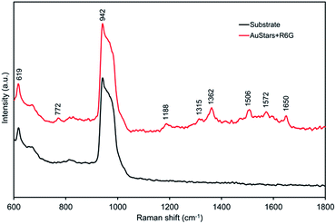 | ||
| Fig. 1 Example of the Raman spectrum of Rhodamine 6G obtained on a substrate comprised of 400 nm diameter Au circles. A spectrum from a nearby region of the naked substrate is also shown. | ||
The Raman signal strengths obtained over the wide range of shapes used were exceedingly variable: essentially, the area under the 1362 cm−1 R6G peak could be anything between 900 and 120![[thin space (1/6-em)]](https://www.rsc.org/images/entities/char_2009.gif) 000 units (
000 units (![[x with combining macron]](https://www.rsc.org/images/entities/i_char_0078_0304.gif) was 18
was 18![[thin space (1/6-em)]](https://www.rsc.org/images/entities/char_2009.gif) 800 and s = 22
800 and s = 22![[thin space (1/6-em)]](https://www.rsc.org/images/entities/char_2009.gif) 040). This variability, and in particular the apparently random appearance of extremely high enhancements, is a widely reported problem with SERS2,5,8 and, indeed, is the issue that we are attempting to resolve in the present work by use of the lithographically-produced patches. We explored the results further to try identify any trends in the signal strength with regard to shape, size or spacing of the patches. There was no correlation between intensity of SERS signal and the relative coverage of Au (r2 < 0.1). (Some correlation with coverage of Au would have occurred if the enhancement of these large flat patches had been dominated by chemical enhancement or the surface roughness effect as described by Sow et al.9) An increase in the inter-patch gap distance from the minimum of 100 nm was also found to have no statistically significant effect on the SERS enhancement. (Indeed, none was expected, as the 633 nm excitation wavelength was far away from the dipolar LSPRs wavelengths of these shapes.) There was no effect of grid symmetry (hexagonal vs. square, probably for the same reason as for the lack of effect of the gap distance). Finally, there was no correlation with patch perimeter length (r2 < 0.1) (a strong correlation would have indicated that the location of the enhancing phenomenon was spread evenly along the edges of the patches).
040). This variability, and in particular the apparently random appearance of extremely high enhancements, is a widely reported problem with SERS2,5,8 and, indeed, is the issue that we are attempting to resolve in the present work by use of the lithographically-produced patches. We explored the results further to try identify any trends in the signal strength with regard to shape, size or spacing of the patches. There was no correlation between intensity of SERS signal and the relative coverage of Au (r2 < 0.1). (Some correlation with coverage of Au would have occurred if the enhancement of these large flat patches had been dominated by chemical enhancement or the surface roughness effect as described by Sow et al.9) An increase in the inter-patch gap distance from the minimum of 100 nm was also found to have no statistically significant effect on the SERS enhancement. (Indeed, none was expected, as the 633 nm excitation wavelength was far away from the dipolar LSPRs wavelengths of these shapes.) There was no effect of grid symmetry (hexagonal vs. square, probably for the same reason as for the lack of effect of the gap distance). Finally, there was no correlation with patch perimeter length (r2 < 0.1) (a strong correlation would have indicated that the location of the enhancing phenomenon was spread evenly along the edges of the patches).
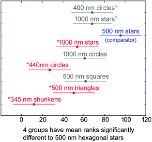
The results for the nine different shapes were also scattered. As the enhancement data for peak areas were in general not normally distributed (ESI, Fig. S2†), a non-parametric Kruskal–Wallis statistical analysis was conducted, Fig. 2. In this analysis the relative ranking of the different populations are examined. This showed that the 500 nm wide stars gave the best performance, with this verdict passing the α = 0.05 (95% confidence) level relative to four of the other eight patch designs. The shuriken array was the worst performer, being inferior to six of the eight other shapes at the same level of confidence.
Calculated enhancements
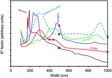
The calculations show that, due to the non-linear effect of taking the 4th power of E, almost all the SERS enhancement effect is localized to the immediate vicinity of the nanopatches, especially their edges, in agreement with the prior literature.9 The electric field above the top surface of the gold target is weak, generally weaker even than that above the Si substrate. Secondly, it is clear that the values of the average ‖E‖4 parameter do not vary systematically or monotonically with shape or size of shape and, instead, there are some specific optima. The enhancement trends for an excitation wavelength of 633 nm are summarized for the different shapes in Fig. 3. (Detailed results for circles and hollow hex stars are provided in the ESI, Fig. S4†). The average ‖E‖4 values corresponding to the shuriken and smaller circles tested are approximately the same, but 500 nm squares and 1000 nm circles are predicted to be relatively inferior. One surprise is that the 500 nm triangles are predicted to be twice as effective at providing enhancement as the 500 nm stars. This is the opposite of what was observed. The most probable reason for this is that the relatively narrow multipolar resonance in the triangles may not have been activated in the experimental shapes due to its position being slightly different from the 633 nm predicted in the simulations. Overall, it seems that triangles or stars in the 200 to 300 nm size range would be the best choice, however the spread in values between worst performer and best performer is generally less than a factor of 3 or 4. The very narrow range of sizes in the squares that produce good enhancement is also worth noting.The simulations also confirm that direction of polarization of normally incident light does not have much effect on the average ‖E‖4 of equilateral triangles (ESI, Fig. S5†), and by extension, the other shapes with 3-fold or greater rotational symmetry.
In addition, examination of the electric field distributions confirms that each of the maxima in ‖E‖4 in Fig. 3 can be matched to a strong multipolar resonance that is tuned to the 633 nm excitation wavelength in the relevant patch. In contrast, the lowest values of average ‖E‖4 are associated with an absence of a strong near-field resonance at 633 nm. The electric field for a 310 nm diameter circle is shown in Fig. 4 in cross-section (see also Video 1 in ESI†), whilst that for 250 and 483 nm triangles is shown in Fig. 5 on the reference plane used for the calculation of the average ‖E‖4.
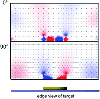 | ||
| Fig. 4 Multipolar resonance of 310 nm disk on silicon substrate, visualized in cross-section, and at two different times (phase angles) in the oscillation. | ||
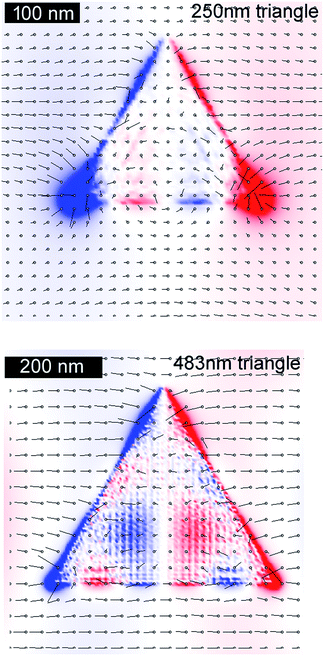 | ||
| Fig. 5 Multipolar resonance caused by 633 nm excitation of equilateral triangles with bases of 250 and 483 nm, visualized at phase angles of 120° and 45° respectively. | ||
Overall, the SERS effect in the presence patches cannot be due to the development of a dipolar localized surface plasmon resonance as all of them are so large and flat that their dipolar resonances lie well beyond the 633 nm excitation wavelength. For example, the 310 nm circle has a dipolar LSPR at 930 nm when suspended in vacuum and this is red-shifted to about 1730 nm when it is placed on top of the silicon slab.
The multipole effect is clearly an important component of the SERS response and may be more significant than the effects of having protrusions or surface roughness on the stars. It also explains why specific diameters of circles and stars can be significantly better enhancers of the SERS effect than others.
The non-linear response of the SERS signal to size of patch correlates with our experience of variability in the experimental data. It is likely, for example, that the superior performance of the 500 nm wide stars compared to that of the other shapes resulted from the 633 nm excitation exciting a stronger multipolar resonance in that shape than in the others. It is also important to note that, as it is a multipolar LSPR that is producing the SERS, the hot spots are not necessarily located at the tips of the patch. However, all else being equal, a stronger SERS signal would still be expected from a dipolar resonance which inevitably does have its hot spots at the opposing extremities or tips of the patch. In addition, the strength of the near-field of a dipolar resonance is sustained to a greater distance from the patch surface than is the case for multipolar resonances, (ESI, Fig. S6†).
Nevertheless, the simulations show that the multipolar resonances on large gold patches are also a viable option for SERS. In general, triangles and stars are likely to be better options in this case than circles or squares, provided that their multipolar resonances are tuned onto the Raman excitation wavelength by careful control of the geometry. The triangular motif in particular potentially offers two strong multipolar resonances under the conditions assumed in this study.
Conclusions
While both geometry (shape and size) and surface roughness certainly have a role to play in enhancing the Raman signal on Au shapes produced by EBL, these effects are masked by the stochastic variation in experimental measurements. The present data indicated at the 95% confidence level that the 500 nm wide hollow hexagonal nanostars were superior to the most of other shapes tested, whilst the 350 nm wide shurikens were inferior to most of the other shapes tested. No statistically significant difference in Raman enhancement could be found between the various circles, squares and triangles.We probed this phenomenon further using electromagnetic simulations of models of these shapes on a silicon substrate. In all cases the dipolar plasmon resonance of these shapes lay in the near-infrared and hence could never play a role in electromagnetic enhancement of any Raman signals excited with 633 nm light. However, it was clear that significant enhancement at visible excitation wavelengths could still be expected if the size and geometry of the Au shape was carefully adjusted so that it would have a multipolar plasmon resonance at the Raman excitation wavelength. This is likely to be the reason for the superior performance of the 500 nm wide hollow hexagonal stars compared to that of the other shapes tested.
The results also show that the far-field optical properties of an array are a poor predictor for its efficacy. The insights provided here will be of use to others wishing to design SERS substrates produced by electron beam lithography.
Acknowledgements
We thank Dr Elizabeth Neall (University of Wollongong) for advice on statistical analysis, Dr Sujeewa de Silva and Dr Linda Xiao (University of Technology Sydney) for assisting with SEM and SERS analyses, and Dr Han-Hao Cheng and Dr Idriss Blakey (Australian Institute for Bioengineering and Nanotechnology, University of Queensland) for assistance with the electron beam lithography. S. Z. acknowledges post-doctoral fellowships from University of Queensland, and University of Technology Sydney under Australian Research Council grant DP120102545. Samples were fabricated at the University of Queensland node of the Australian National Fabrication Facility (ANFF-Q), a company established under the National Collaborative Research Infrastructure Strategy of Australia. Computer time was provided by Australia's National Computational Infrastructure (NCI).Notes and references
- C. L. Haynes, A. D. McFarland and R. P. V. Duyne, Anal. Chem., 2005, 338A–346A CAS.
- M. Fan and A. G. Brolo, Phys. Chem. Chem. Phys., 2009, 11, 7381–7389 RSC.
- K. Kneipp, Y. Wang, H. Kneipp, L. T. Perelman, I. Itzkan, R. R. Dasari and M. S. Feld, Phys. Rev. Lett., 1997, 78, 1667–1670 CrossRef CAS.
- S. Nie and S. R. Emory, Science, 1997, 275, 1102–1106 CrossRef CAS PubMed.
- P. Etchegoin, L. F. Cohen, H. Hartigan, R. J. C. Brown, M. J. T. Milton and J. C. Gallop, J. Chem. Phys., 2003, 119, 5281–5289 CrossRef CAS.
- R. A. Alvarez-Puebla, D. J. Ross, G. A. Nazri and R. F. Aroca, Langmuir, 2005, 21, 10504–10508 CrossRef CAS PubMed.
- M. Chirumamilla, A. Gopalakrishnan, A. Toma, R. P. Zaccaria and R. Krahne, Nanotechnology, 2014, 25, 235303 CrossRef PubMed.
- N. Guillot and M. L. d. l. Chapelle, J. Quant. Spectrosc. Radiat. Transfer, 2012, 113, 2321–2333 CrossRef CAS.
- I. Sow, J. Grand, G. Lévi, J. Aubard, N. Félidj, J.-C. Tinguely, A. Hohenau and J. R. Krenn, J. Phys. Chem. C, 2013, 117, 25650–25658 CAS.
- D. L. Jeanmaire and R. P. Van-Duyne, J. Electroanal. Chem., 1977, 84, 1–20 CrossRef CAS.
- N. Félidj, J. Aubard and G. Lévi, Phys. Rev. B: Condens. Matter Mater. Phys., 2002, 66, 245407 CrossRef.
- W. Yue, Z. Wang, Y. Yang, L. Chen, A. Syed, K. Wong and X. Wang, J. Micromech. Microeng., 2012, 22, 125007 CrossRef.
- L. Billot, M. L. d. l. Chapelle, A.-S. Grimault, A. Vial, D. Barchiesi, J.-L. Bijeon, P.-M. Adam and P. Royer, Chem. Phys. Lett., 2006, 422, 303–307 CrossRef CAS.
- J. A. Dieringer, A. D. McFarland, N. C. Shah, D. A. Stuart, A. V. Whitney, C. R. Yonzon, M. A. Young, X. Zhang and R. P. V. Duyne, Faraday Discuss., 2005, 132, 9–26 RSC.
- J. Liu, A. I. Maaroof, L. Wieczorek and M. B. Cortie, Adv. Mater., 2005, 17, 1276–1281 CrossRef CAS.
- J. Liu, B. Cankurtaran, G. McCredie, M. Ford, L. Wieczorek and M. Cortie, Nanotechnology, 2005, 16, 3023–3028 CrossRef CAS.
- J. S. Shumaker-Perry, H. Rochholz and M. Kreiter, Adv. Mater., 2005, 17, 2131–2134 CrossRef.
- V. Giannini, R. Rodríguez-Oliveros and J. A. Sánchez-Gil, Plasmonics, 2010, 5, 99–104 CrossRef.
- P. F. Liao and A. Wokaun, J. Chem. Phys., 1982, 76, 751–752 CrossRef CAS.
- S. Zhu, M. Cortie and I. Blakey, Nanomater. Nanotechnol., 2015, 5, 22 CrossRef.
- M. D. Doherty, A. Murphy, R. J. Pollard and P. Dawson, Phys. Rev. X, 2013, 3, 011001 Search PubMed.
- S. Zhu, H.-H. Cheng, I. Blakey, N. Stokes, K. Ostrikov and M. Cortie, Microelectron. Eng., 2015, 139, 13–18 CrossRef CAS.
- A. M. Schwartzberg, C. D. Grant, A. Wolcott, C. E. Talley, T. R. Huser, R. Bogomolni and J. Z. Zhang, J. Phys. Chem. B, 2004, 108, 19191–19197 CrossRef CAS.
- J. Gao, Y. Hua, S. Li, Y. Zhang and X. Chen, Spectrochim. Acta, Part A, 2013, 104, 41–47 CrossRef CAS PubMed.
- J. A. Dieringer, K. L. Wustholz, D. J. Masiello, J. P. Camden, S. L. Kleinman, G. C. Schatz and R. P. V. Duyne, J. Am. Chem. Soc., 2009, 131, 849–854 CrossRef CAS PubMed.
- B. T. Draine and P. J. Flatau, J. Opt. Soc. Am. A, 1994, 11, 1491–1499 CrossRef.
- B. T. Draine and P. J. Flatau, J. Opt. Soc. Am. A, 2008, 25, 2693–2703 CrossRef PubMed.
- C. Novo, A. M. Funston, I. Pastoriza-Santos, L. M. Liz-Marzán and P. Mulvaney, J. Phys. Chem. C, 2008, 112, 3–7 CAS.
- M. W. Knight, Y. Wu, J. B. Lassiter, P. Nordlander and N. J. Halas, Nano Lett., 2009, 9, 2188–2192 CrossRef CAS PubMed.
- S. Zhu and W. Zhou, J. Opt., 2011, 40, 65–70 CrossRef.
- B. Hopkins, W. Liu, A. E. Miroshnichenko and Y. S. Kivshar, Nanoscale, 2013, 5, 6395–6403 RSC.
- G. Fletcher, M. D. Arnold, T. Pedersen, V. J. Keast and M. B. Cortie, Opt. Express, 2015, 23, 18002–18013 Search PubMed.
- L. Jensen and G. C. Schatz, J. Phys. Chem. A, 2006, 110, 5973–5977 CrossRef CAS PubMed.
- H. Watanabe, N. Hayazawa, Y. Inouye and S. Kawata, J. Phys. Chem. B, 2005, 109, 5012–5020 CrossRef CAS PubMed.
- A. Zwick and R. Caries, Phys. Rev. B: Condens. Matter Mater. Phys., 1993, 48, 6024–6032 CrossRef CAS.
Footnotes |
| † Electronic supplementary information (ESI) available: SEM images of gold patches, plot of SERS peak areas illustrating log-normal statistics, plots of E4vs. size of shape, graphs showing effect of orientation of shapes. See DOI: 10.1039/c6ra22450d |
| ‡ The far-field optical properties are those observed by techniques conducted a large distance (many wavelengths) away from the sample surface. Examples include reflectance and transmittance. In contrast, observation of near-field optical properties requires the application of sophisticated techniques such as near-field scanning optical microscopy or electron energy loss spectroscopy. These probe the field within a few nanometers from the surface. |
| This journal is © The Royal Society of Chemistry 2016 |

