Room-temperature mixed-solvent-vapor annealing for high performance perovskite solar cells†
Hao
Yu
a,
Xiaodong
Liu
a,
Yijun
Xia
a,
Qingqing
Dong
a,
Kaicheng
Zhang
a,
Zhaowei
Wang
a,
Yi
Zhou
*a,
Bo
Song
*a and
Yongfang
Li
*ab
aLaboratory of Advanced Optoelectronic Materials, College of Chemistry, Chemical Engineering and Materials Science, Soochow University, Suzhou, 215123, China. E-mail: yizhou@suda.edu.cn; songbo@suda.edu.cn
bBeijing National Laboratory for Molecular Sciences, Institute of Chemistry, Chinese Academy of Sciences, Beijing, 100190, China. E-mail: liyf@iccas.ac.cn
First published on 18th November 2015
Abstract
In this paper, we introduce a room-temperature mixed-solvent-vapor annealing (rtMSVA) method to fabricate high performance perovskite solar cells (pero-SCs) based on MAPbI3−xClx without the need for thermal annealing (TA). An ultra-smooth perovskite thin-film with high crystallinity was obtained by the DMF/CB mixed-solvent (1![[thin space (1/6-em)]](https://www.rsc.org/images/entities/char_2009.gif) :
:![[thin space (1/6-em)]](https://www.rsc.org/images/entities/char_2009.gif) 20, v/v) vapor annealing at room-temperature without TA and the power conversion efficiency (PCE) of the pero-SCs reached 16.4%. More importantly, the reproducibility of the PCEs is quite good among 40 different devices. Furthermore, large active area pero-SCs were fabricated with the rtMSVA method. The PCEs of the pero-SCs based on ITO and flexible PET/Ag mesh electrodes with an active area of 1.21 cm2 reached 11.01% and 7.5%, respectively. We anticipate that rtMSVA would very possibly become a promising crystallization method for the fabrication of large area pero-SCs in the near future.
20, v/v) vapor annealing at room-temperature without TA and the power conversion efficiency (PCE) of the pero-SCs reached 16.4%. More importantly, the reproducibility of the PCEs is quite good among 40 different devices. Furthermore, large active area pero-SCs were fabricated with the rtMSVA method. The PCEs of the pero-SCs based on ITO and flexible PET/Ag mesh electrodes with an active area of 1.21 cm2 reached 11.01% and 7.5%, respectively. We anticipate that rtMSVA would very possibly become a promising crystallization method for the fabrication of large area pero-SCs in the near future.
Introduction
Perovskite solar cells (pero-SCs) are nowadays experiencing a rapid development, and have become a very hot research area.1–8 Since the first report by Miyasaka et al. in 2009, the power conversion efficiency (PCE) of pero-SCs has skyrocketed from 3.8% to 20.1%.9–13 Organic–inorganic hybrid perovskite possesses many outstanding photovoltaic features, such as high absorption coefficient, long exciton diffusion length, low exciton binding energy and high charge carrier mobility.14–19 Nevertheless, the photovoltaic performance (e.g., PCE, reproducibility and hysteresis) of the pero-SCs strongly depends on the quality (morphology and crystallization) of the perovskite (e.g. MAPbI3−xClx) active layers.20–23 To date, several preparation methods, such as two-step sequential deposition,24–26 one-step spin-coating,27 dual-source evaporation,20 a vapor-assisted solution process,28 mix-solvent engineering,29 colloidal chemistry,30 additive enhancement,31,32etc., have been successfully employed to obtain high quality perovskite thin-films (pero-TFs). In almost all the preparation methods, no matter how a pero-TF was processed, thermal annealing (TA) was routinely conducted to induce the crystallization of pero-TFs. The temperature and time period for TA treatment varied from paper to paper, although a typical temperature of 95 °C and several hours are commonly used for obtaining a high quality film.21 During TA processing, the crystal growth of pero-TFs is controlled by heterogeneous nucleation, thus it is difficult to obtain an ultra-smooth pero-TF by the TA treatment. In addition, the TA treatment is time- and energy-consuming, sometimes decomposes the perovskite films, and it is inconvenient for massive production. Therefore, exploring an alternative method to induce the crystallization of pero-TFs without the need for TA treatment is highly demanded.In this regard, some efforts have been made to develop a new processing method for the preparation of crystalline pero-TFs by a couple of groups recently. For example, Xiao et al. reported a fast deposition-crystallization (FDC) procedure, where they dripped an extra solvent during the high-speed spin-coating process to induce crystallization.33 Analogous treatments were also employed in the earlier reports by Jeon et al.29 and Jung et al.,34 which were helpful to create smooth pero-TFs. Xiao and Huang et al. reported a solvent annealing method by using dimethylformamide (DMF) solvent vapor for increasing the crystal size of the perovskite to improve photovoltaic performances of the pero-SCs.35 However, TA treatment was still needed in these experiments.
Notably, Zhou et al. developed a solvent–solvent extraction (SSE) procedure to realize the rapid crystallization of perovskite, and obtained uniform, ultra-smooth pero-TFs.36 The SSE processing can be conducted at room temperature, and no TA treatment was involved. The second solvent used in the SSE method for extraction of N-methyl-2-pyrrolidone (NMP, a solvent for perovskite precursors) was diethyl ether, which is a poor solvent of methyl ammonium iodide (MAI). As NMP was extracted, the pero-TF was “frozen” at the same time. Since the extraction was performed in a very short time (typically 2 min, or even less) and there is no annealing process in the SSE method, the crystallinity of the film needs to be improved.
Herein, we present a room-temperature mixed-solvent-vapor annealing (rtMSVA) method to induce the crystallization of pero-TFs in the fabrication of planar p-i-n pero-SCs based on MAPbI3−xClx with the device structure of ITO/PEDOT:PSS/pero-TF/PCBM/LiF/Al. The mixed solvents of DMF and chlorobenzene (CB) with an appropriate volume ratio were used in the rtMSVA treatment and the treatment was conducted at room temperature for a few minutes without the need for TA processing. Through this simple process, ultra-smooth and highly crystalline pero-TFs were obtained. For small active area (0.04 cm2) pero-SCs, the maximum PCE reached was 16.4% and an average PCE was 15.2% with a very narrow standard deviation of 0.6% within 40 devices. We also fabricated large active area (LAA) pero-SCs with an active area of 1.21 cm2 on ITO or flexible PET/Ag wire/electrodes with the rtMSVA method, an average PCE of 9.77 ± 0.65% and 7.5% were achieved for the devices based on ITO and flexible electrodes, respectively. To the best of our knowledge, 7.5% is the highest PCE reported so far for such LAA flexible pero-SCs. Clearly, the rtMSVA is a promising method for the fabrication of pero-SCs, especially for the production of LAA flexible pero-SCs.
Results and discussion
It is well known that the color of MAPbI3−xClx perovskite thin films (pero-TFs) turns from yellow to dark brown as a result of the TA treatment. This characteristic feature was commonly used to judge the crystallization of MAPbI3−xClx into the perovskite phase during the preparation of pero-SCs. The same phenomenon was observed when we use the rtMSVA treatment with the mixed solvent of DMF/CB (1![[thin space (1/6-em)]](https://www.rsc.org/images/entities/char_2009.gif) :
:![[thin space (1/6-em)]](https://www.rsc.org/images/entities/char_2009.gif) 20, v/v). The color of the as-spin-coated MAPbI3−xClx film changed rapidly in the vapor atmosphere of the DMF/CB mixture. Typically, it took only a few minutes to convert the color of the film from yellow to dark brown (indicating the conversion to the perovskite phase of the film), as shown in Fig. S1 in the ESI.†Fig. 1 shows the time-dependent UV-vis absorption spectra of the MAPbI3−xClx films before and after the rtMSVA treatment of DMF/CB (1
20, v/v). The color of the as-spin-coated MAPbI3−xClx film changed rapidly in the vapor atmosphere of the DMF/CB mixture. Typically, it took only a few minutes to convert the color of the film from yellow to dark brown (indicating the conversion to the perovskite phase of the film), as shown in Fig. S1 in the ESI.†Fig. 1 shows the time-dependent UV-vis absorption spectra of the MAPbI3−xClx films before and after the rtMSVA treatment of DMF/CB (1![[thin space (1/6-em)]](https://www.rsc.org/images/entities/char_2009.gif) :
:![[thin space (1/6-em)]](https://www.rsc.org/images/entities/char_2009.gif) 20, v/v) for different time periods. For the as-spin-coated MAPbI3−xClx film, the absorption is mainly located in the wavelength region lower than 600 nm. After being treated with rtMSVA, the absorption spectrum red-shifted significantly and the absorption band extended to a longer wavelength up to 800 nm when the treatment time period was longer than 4 minutes. The maximum absorption intensity and the broadest absorption range were reached in approximately 6 minutes (Fig. 1). Further elongation of the time period of rtMSVA processing did not cause a significant difference in the absorption spectra, indicating that the crystallization was completed in ca. 6 minutes. Therefore, 6 minutes rtMSVA was adopted during the fabrication of pero-SCs. It is noteworthy that this rtMSVA treatment was in all cases conducted under room temperature, and no further thermal annealing treatment was needed afterwards.
20, v/v) for different time periods. For the as-spin-coated MAPbI3−xClx film, the absorption is mainly located in the wavelength region lower than 600 nm. After being treated with rtMSVA, the absorption spectrum red-shifted significantly and the absorption band extended to a longer wavelength up to 800 nm when the treatment time period was longer than 4 minutes. The maximum absorption intensity and the broadest absorption range were reached in approximately 6 minutes (Fig. 1). Further elongation of the time period of rtMSVA processing did not cause a significant difference in the absorption spectra, indicating that the crystallization was completed in ca. 6 minutes. Therefore, 6 minutes rtMSVA was adopted during the fabrication of pero-SCs. It is noteworthy that this rtMSVA treatment was in all cases conducted under room temperature, and no further thermal annealing treatment was needed afterwards.
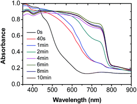 | ||
Fig. 1 Time-dependent UV-vis absorption spectra of the MAPbI3−xClx thin films before and after the rtMSVA of DMF/CB with a volume ratio of 1![[thin space (1/6-em)]](https://www.rsc.org/images/entities/char_2009.gif) : :![[thin space (1/6-em)]](https://www.rsc.org/images/entities/char_2009.gif) 20. 20. | ||
It should be mentioned that the mixed solvent of DMF/CB is crucial for the room-temperature solvent annealing. The single solvent of DMF or CB cannot turn the as-spin-coated MAPbI3−xClx thin films into perovskite structures by the solvent annealing at room temperature. Fig. S1 in the ESI† shows the photographs of the sample plates before and after the solvent annealing at room temperature by the mixed solvent of DMF/CB (1![[thin space (1/6-em)]](https://www.rsc.org/images/entities/char_2009.gif) :
:![[thin space (1/6-em)]](https://www.rsc.org/images/entities/char_2009.gif) 20 v/v) or the single solvent of DMF or CB. As mentioned above, the color of the sample film was changed from yellow to dark brown after 6 minutes rtMSVA, but the color of the as-spin-coated MAPbI3−xClx film changed to colorless after 10 seconds room-temperature solvent annealing by the single solvent of DMF, and remained unchanged after the room-temperature solvent annealing of CB for 10 minutes. The weak effect of CB processing can be further confirmed by the small differences of absorption spectra of the MAPbI3−xClx thin films before and after treatment, as shown in Fig. S2 in the ESI.†
20 v/v) or the single solvent of DMF or CB. As mentioned above, the color of the sample film was changed from yellow to dark brown after 6 minutes rtMSVA, but the color of the as-spin-coated MAPbI3−xClx film changed to colorless after 10 seconds room-temperature solvent annealing by the single solvent of DMF, and remained unchanged after the room-temperature solvent annealing of CB for 10 minutes. The weak effect of CB processing can be further confirmed by the small differences of absorption spectra of the MAPbI3−xClx thin films before and after treatment, as shown in Fig. S2 in the ESI.†
The crystallinity of pero-TFs is a crucial parameter, which is correlated to the light-absorption ability, charge transport and recombination properties of the pero-SCs. High crystallinity will lead to high performance of the resulting devices. Fig. 2 shows XRD patterns of the pero-TFs treated by rtMSVA and TA, respectively. With similar film thickness and under the same measurement conditions, the diffraction peak intensity of the pero-TFs processed by rtMSVA was several times higher than that of the pero-TFs by TA treatment.
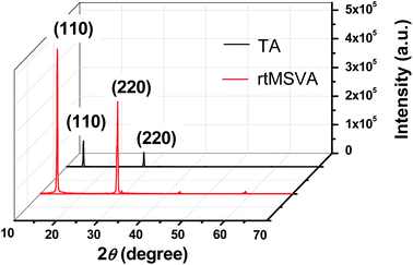 | ||
Fig. 2 XRD patterns of the pero-TFs treated by TA at 95 °C for 2 hours and by rtMSVA of DMF/CB mixed solvents with a volume ratio of 1![[thin space (1/6-em)]](https://www.rsc.org/images/entities/char_2009.gif) : :![[thin space (1/6-em)]](https://www.rsc.org/images/entities/char_2009.gif) 20 for 6 minutes. 20 for 6 minutes. | ||
In general, XRD peak intensity is related to the crystal orientation and surface porosity. The FWHM values of the strong diffraction peaks of the (110) face were calculated using JADE 5.0 to evaluate the grain size. The FWHM values of the perovskite films prepared with rtMSVA and TA treatment are 0.207 and 0.173, respectively. According to Scherrer's equation, the grain size of the perovskite films prepared with rtMSVA treatment is slightly smaller than that with TA treatment. According to the diffraction peak intensity of the pero-TFs, we optimized the volume ratio of the DMF/CB mixed solvents in the rtMSVA treatment. We found that the diffraction peak intensity was strong for the pero-TFs treated by the rtMSVA with a DMF/CB volume ratio from 1![[thin space (1/6-em)]](https://www.rsc.org/images/entities/char_2009.gif) :
:![[thin space (1/6-em)]](https://www.rsc.org/images/entities/char_2009.gif) 25 to 1
25 to 1![[thin space (1/6-em)]](https://www.rsc.org/images/entities/char_2009.gif) :
:![[thin space (1/6-em)]](https://www.rsc.org/images/entities/char_2009.gif) 15, but the pero-TFs treated by the rtMSVA with a DMF/CB volume ratio of 1
15, but the pero-TFs treated by the rtMSVA with a DMF/CB volume ratio of 1![[thin space (1/6-em)]](https://www.rsc.org/images/entities/char_2009.gif) :
:![[thin space (1/6-em)]](https://www.rsc.org/images/entities/char_2009.gif) 20 (see Fig. S3 in the ESI†) displayed the strongest diffraction peak intensity at faces [100] and [200]. Therefore in the following, the volume ratio of 1
20 (see Fig. S3 in the ESI†) displayed the strongest diffraction peak intensity at faces [100] and [200]. Therefore in the following, the volume ratio of 1![[thin space (1/6-em)]](https://www.rsc.org/images/entities/char_2009.gif) :
:![[thin space (1/6-em)]](https://www.rsc.org/images/entities/char_2009.gif) 20 of the DMF/CB mixed solvents was used in the rtMSVA treatment.
20 of the DMF/CB mixed solvents was used in the rtMSVA treatment.
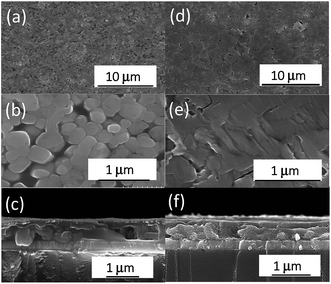
Morphology is another property for characterizing the quality of pero-TFs. Fig. 3 shows the SEM images of the pero-TFs treated by rtMSVA and TA. After treatment with rtMSVA, an almost pinhole-free film is demonstrated, and the pero-TF is composed of well-defined crystalline particles of sub-micrometer size. In a control experiment, the samples processed by TA had some pinholes and even cracks in the film. Based on both the enhanced diffraction peak intensity and the improved morphology of the pero-TFs, we can expect that rtMSVA treatment could lead to higher photovoltaic performances of the pero-SCs.
In the following, rtMSVA was applied in fabrication of planar p-i-n pero-SCs based on MAPbI3−xClx, and the photovoltaic performance was compared with the devices treated by TA. To make a parallel comparison with the previously published literature, the small area devices with an active area of 0.04 cm2 were firstly prepared. The device configuration of the planar p-i-n pero-SCs is ITO/PEDOT:PSS/MAPbI3−xClx/PCBM/LiF/Al. Fig. 4 presents the J–V curves of the pero-SCs under the illumination of AM 1.5G, 100 mW cm−2, and the EQE spectra of the devices processed by rtMSVA and TA, respectively. The corresponding photovoltaic parameters are listed in Table 1. The open-circuit voltage (Voc) of the devices with rtMSVA treatment was much higher (∼1 V) than those with TA treatment (0.91 V), which may be ascribed to the higher crystallinity of the pero-TFs treated by rtMSVA.
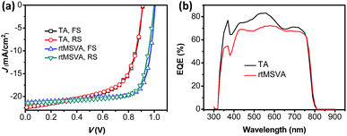 | ||
Fig. 4 (a) FS/RS J–V curves and (b) EQE spectra of pero-SCs separately treated with TA at 95 °C for 2 hours and rtMSVA of DMF/CB (1![[thin space (1/6-em)]](https://www.rsc.org/images/entities/char_2009.gif) : :![[thin space (1/6-em)]](https://www.rsc.org/images/entities/char_2009.gif) 20 v/v) for 6 minutes. 20 v/v) for 6 minutes. | ||
| MAPbI3−xClx | V oc (V) | J sc (mA cm−2) | FF (%) | PCE (%) | |
|---|---|---|---|---|---|
| TA | FS | 0.91 | 22.37 | 62.5 | 12.73 |
| RS | 0.91 | 22.39 | 62.6 | 12.76 | |
| rtMSVA | FS | 1.01 | 21.30 | 76.5 | 16.41 |
| RS | 1.00 | 21.46 | 75.5 | 16.16 | |
| rtMSVA (statistics) | 1.01 ± 0.01 | 20.42 ± 0.48 | 73.2 ± 1.8 | 15.2 ± 0.60 |
Meanwhile, the fill factor (FF) changes in the same trend, it is 76% for the device with rtMSVA treatment and 66% for that with TA treatment. The higher FF for the pero-SCs treated by rtMSVA could be attributed to a lower leakage current. For further explanation of the phenomenon, the series resistances (Rs) and shunt resistances (Rsh) of the devices were calculated from the slope of the J–V curves at 0 mA cm−2 and 0 V, respectively. Rs & Rsh of the pero-SC with rtMSVA and TA treatment were 2.62 & 699.0 Ω cm−2 and 4.38 & 243.9 Ω cm−2, respectively. The larger Rsh in the rtMSVA-treated pero-SCs should lead to a lower leakage current and higher FF.
A slight decrease of the short-circuit current (Jsc) was observed both in the J–V curves and integrations of EQE spectra for the rtMSVA-treated pero-SCs. According to the EQE in Fig. 4b, the integrated Jsc for rtMSVA- and TA-treated devices are 18.8 and 19.4 mA cm−2, respectively. The values, show the same trend as that indicated by J–V curves, although they are lower than the Jsc values from J–V curves. The lower Jsc values calculated from EQE can be explained by the degradation of the pero-SCs being exposed to air during the EQE measurement.
The optimal PCE of the pero-SC with rtMSVA treatment was 16.41% with a Voc, Jsc and FF of 1.01 V, 21.46 mA cm−2 and 76.5%, respectively. The average PCE analyzed from 40 cells (Fig. S4 in the ESI†) was 15.2 (±0.60)%, with an average Voc, Jsc and FF of 1.01 (±0.01) V, 20.42 (±0.48) mA cm−2, and 73.2 (±1.8)%, respectively. The standard deviations of the J–V characteristics were all very small. Notably, the Voc values were maintained at slightly higher than 1.0 V. The good reproducibility of the photovoltaic performance indicates that rtMSVA is a reliable annealing method to induce the crystallization of pero-TFs.
It is often reported in the literature that the J–V curves of the pero-SCs obtained from a forward-scan (FS, the scan from a lower voltage to a higher voltage) and reverse-scan (RS, the scan from a higher voltage to a lower voltage) were not consistent. This phenomenon is called hysteresis, and often happens to the n-i-p type pero-SCs (ITO as the cathode). Here the p-i-n type configuration was adopted, and the hysteresis did not appear in the J–V curves of the devices with pero-TFs processed by rtMSVA and TA (see Fig. 4a).
It should be mentioned that after the rtMSVA treatment we waited for a period of approximately 12 h to allow any remaining trace amount of the solvent to dry off before preparing the top electrode for high performance pero-SCs. The photovoltaic performance of the pero-SC will be lower if the pero-TF was not dried for 12 h after rtMSVA treatment.
The advantages of rtMSVA, such as simple room temperature treatment, high quality pero-FTs and good reproducibility of the photovoltaic performance, are attractive for the fabrication of LAA solar cells. Therefore, we fabricated the LAA pero-SCs on both ITO glass and PET/Ag-grid substrates with an active area of 1.21 cm2, and the photovoltaic performance of the devices was characterized.
For the LAA pero-SCs based on ITO glass, the device configuration and preparation procedure were the same with that of the small area devices, but with a larger area of the top electrode (the aluminum electrode). The J–V curve for the best performance device treated by rtMSVA is shown in Fig. 5. The peak PCE was 11.01%, with a Voc, Jsc and FF of 1.01 V, 20.29 mA cm−2 and 53.5%, respectively. The relatively lower FF of the LAA pero-SCs could be due to the larger sheet resistance of the transparent electrode. The average PCE analyzed from 20 cells was 9.77 (±0.65)%, with a Voc, Jsc and FF of 1.00 (±0.01) V, 21.17 (±1.52) mA cm−2 and 46.3 (±4.2)%, respectively. Similar to small area pero-SCs based on ITO glass, the deviations of the parameters were quite small, further confirming that rtMSVA leads to a good reproducibility of the device performances.
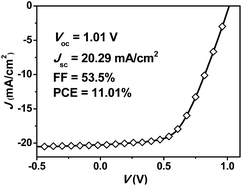 | ||
Fig. 5
J–V curve of the pero-SC with an active area of 1.21 cm2, processed by rtMSVA of DMF/CB (1![[thin space (1/6-em)]](https://www.rsc.org/images/entities/char_2009.gif) : :![[thin space (1/6-em)]](https://www.rsc.org/images/entities/char_2009.gif) 20 v/v) for 6 minutes. 20 v/v) for 6 minutes. | ||
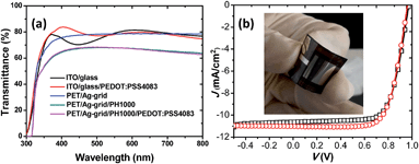
For the flexible LAA pero-SCs based on a PET/Ag-grid, conductivity and transparency are very important for the flexible transparent electrode in the LAA pero-SCs. Therefore, we checked the transparency of the PET/Ag-grid/PH1000 which is used as the flexible transparent electrode in our studies. Fig. 6a presents the transmittance spectra of the ITO glass, ITO glass/PEDOT:PSS, PET/Ag-grid, PET/Ag-grid/PH1000 and PET/Ag-grid/PH1000/PEDOT:PSS. It is clearly shown that the transmittance of the flexible conductive substrates was not as good as the commercialized ITO glass. In the wavelength region of 350−800 nm, the transmittances of the ITO glass and ITO glass/PEDOT:PSS were approximately 80%. After spin-coating a layer of highly conductive PH1000, the transmittance of the PET/Ag-grid/PH1000 substrates decreased to ca. 65%. The loss of transparency will definitely cause reduced performance of the pero-SCs based on these flexible substrates.
We fabricated the flexible LAA pero-SCs with PET/Ag-grid/PH1000 as the flexible transparent electrode. Fig. 6b shows the J–V curves of the pero-SCs with an active area of 1.21 cm2, processed by rtMSVA. Table 2 lists the photovoltaic performance parameters of the devices. The inset in Fig. 6b is a picture of the flexible device. It can be seen from the J–V curves in Fig. 6b and the corresponding photovoltaic characteristics in Table 2 that the hysteresis of the FS and RS J–V curves was neglectable. Both the Voc and FF were rather high, which are comparable with those of the small area devices. The peak PCE of the flexible pero-SCs we have obtained by now is 7.54%. To the best of our knowledge, this efficiency is the highest for such LAA flexible pero-SCs. The only disadvantage of the device was the low Jsc (ca. 11 mA cm−2). Obviously, the lower transmittance of the flexible substrates should be responsible for the relatively smaller Jsc. We speculate that a higher Jsc would be realistically obtained by improving the transparency of the flexible substrates.
![[thin space (1/6-em)]](https://www.rsc.org/images/entities/char_2009.gif) :
:![[thin space (1/6-em)]](https://www.rsc.org/images/entities/char_2009.gif) 20, v/v) for 6 minutes
20, v/v) for 6 minutes
| V oc (V) | J sc (mA cm−2) | FF (%) | PCE (%) | |
|---|---|---|---|---|
| FS | 0.97 | 10.6 | 70.9 | 7.32 |
| RS | 0.96 | 11.0 | 71.2 | 7.54 |
Conclusions
In this work, we introduced a facile rtMSVA treatment method to induce the crystallization of MAPbI3−xClx pero-TFs for high performance pero-SCs. The rtMSVA treatment was carried out with the mixed solvents of DMF/CB (1![[thin space (1/6-em)]](https://www.rsc.org/images/entities/char_2009.gif) :
:![[thin space (1/6-em)]](https://www.rsc.org/images/entities/char_2009.gif) 20, v/v) at room temperature for a short time period (ca. 6 minutes), and did not need the TA treatment. By this processing, ultra-smooth and high crystallinity pero-TFs were obtained. The rtMSVA method is superior compared to the commonly used TA treatment. A peak PCE of 16.4% with good reproducibility was achieved for the pero-SCs based on MAPbI3−xClx with the rtMSVA treatment. Furthermore, the LAA pero-SCs based on ITO and flexible PET/Ag-grid/PH1000 substrates with an active area of 1.21 cm2 by the rtMSVA treatment demonstrated peak PCEs of 11.01% and 7.5%, respectively. The PCE of the device based on flexible PET/Ag-grid/PH1000 is expected to become even higher if the transparency of the substrates could be improved. We anticipate that rtMSVA could very possibly become a dominating crystallization method for high performance pero-SCs in the near future.
20, v/v) at room temperature for a short time period (ca. 6 minutes), and did not need the TA treatment. By this processing, ultra-smooth and high crystallinity pero-TFs were obtained. The rtMSVA method is superior compared to the commonly used TA treatment. A peak PCE of 16.4% with good reproducibility was achieved for the pero-SCs based on MAPbI3−xClx with the rtMSVA treatment. Furthermore, the LAA pero-SCs based on ITO and flexible PET/Ag-grid/PH1000 substrates with an active area of 1.21 cm2 by the rtMSVA treatment demonstrated peak PCEs of 11.01% and 7.5%, respectively. The PCE of the device based on flexible PET/Ag-grid/PH1000 is expected to become even higher if the transparency of the substrates could be improved. We anticipate that rtMSVA could very possibly become a dominating crystallization method for high performance pero-SCs in the near future.
Experimental
Preparation of a perovskite precursor
The MAPbI3−xClx perovskite precursor was synthesized according to the literature.32 One equivalent of hydroiodic acid (57 wt% in water, Aldrich) and 4 equivalents of methylamine (33 wt% in absolute ethanol, Aldrich) were stirred at 0 °C for 2 h. The solvent was removed under reduced pressure. The product MAI was then recrystallized by dissolving it in ethanol and precipitating in diethyl ether for three times, and then dried at 50 °C in a vacuum for 24 h. MAI and PbCl2 (99.999%, Alfa Aesar) were mixed in a molar ratio of 3![[thin space (1/6-em)]](https://www.rsc.org/images/entities/char_2009.gif) :
:![[thin space (1/6-em)]](https://www.rsc.org/images/entities/char_2009.gif) 1 in anhydrous DMF (99.8%, Acros). The final concentration of the perovskite was controlled to ca. 40 wt%. After the reactants were dissolved, 1% 1,8-diiodooctane (DIO, a volume fraction of DMF) was added to the solution. The mixture was stirred overnight at 60 °C under an N2 atmosphere. The solution with the perovskite precursor was stored in a glovebox, and filtrated with 0.45 μm PTFE filters before use.
1 in anhydrous DMF (99.8%, Acros). The final concentration of the perovskite was controlled to ca. 40 wt%. After the reactants were dissolved, 1% 1,8-diiodooctane (DIO, a volume fraction of DMF) was added to the solution. The mixture was stirred overnight at 60 °C under an N2 atmosphere. The solution with the perovskite precursor was stored in a glovebox, and filtrated with 0.45 μm PTFE filters before use.
Fabrication of pero-SCs
Planar p-i-n pero-SCs with the device configuration of ITO/PEDOT:PSS/MAPbI3−xClx/PCBM/LiF/Al. ITO slides (10 Ω per sq., CSG Holding Co., Ltd.) were sonicated sequentially in detergent, Milli-Q water, acetone, ethanol and isopropanol for 10 min each. After being dried, the slides were treated with UV-ozone for 20 min. On the freshly cleaned ITO substrates, PEDOT:PSS (Clevios P VP Al 4083, filtrated with a 0.45 μm nylon filter) was spin-coated and annealed at 150 °C for 15 minutes. The perovskite precursor was deposited on top of PEDOT:PSS by spin-coating at 3000 rpm for 50 s. Then the perovskite layer was treated by rtMSVA or TA methods. (1) rtMSVA treatment. The sample plates of the spin-coated pero-TFs were put in Petri dishes (with a cover but not sealed) with vapors of mixed solvents of DMF and chlorobenzene (CB) with defined volume ratios. The treatment was performed at room temperature without touching the mix-solvent. The color of the pero-TFs turned from yellow to dark brown in a few minutes. The optimized duration was approximately 6 minutes. To obtain high-performance pero-SCs, the rest of the layers of the devices were not immediately covered atop of the pero-TF after the rtMSVA, but we waited for a period of approximately 12 h to allow any remaining trace amount of the solvent to dry off. (2) TA treatment. As a control, the TA process was conducted by putting the specimens on a hot plate maintained at 95 °C for 70−80 minutes. After the rtMSVA or TA treatments, PCBM (15 mg mL−1 in chloroform) was spin-coated at 1200 rpm for 60 s on the pero-TF layers. Then, LiF (∼1 nm) and aluminum (∼100 nm) were sequentially capped on the PCBM layer by vacuum deposition, with a shadow mask clung to the substrates to define the active areas.LAA flexible pero-SCs (with an active area of 1.21 cm2) on a flexible PET/Ag-grid/PH1000 electrode were also fabricated by a similar method as that on an ITO substrate. The device configuration was PET/Ag-grid/PH1000/PEDOT:PSS/MAPbI3−xClx/PCBM/LiF/Al. Note that herein the PET/Ag-grid (supplied by Prof. Zheng Cui) together with a layer of conducting polymer PH1000 was used as the flexible electrode. PET was employed as the flexible support, and the Ag nanoparticles were embedded in the groove-grid carved on the surface of PET. The nominal sheet resistance of the PET/Ag-grid was 2.1 Ω per sq. PH1000 (Clevios) with 5 wt% DMSO was spin coated on the PET/Ag-grid at 600 rpm for 60 s, followed by annealing at 120 °C for 20 min. The remaining operations in the preparation of the flexible pero-SCs are the same as that of the pero-SCs on the ITO substrate.
Measurement and characterization
The time-dependent absorption spectra of pero-TFs during rtMSVA treatment were measured on a Cary 5000 (Agilent) instrument. In order to make a parallel comparison and avoid the influence of ITO, the pero-TFs were deposited on glass/PEDOT:PSS substrates. XRD patterns were collected using an X'Pert-Pro MRD diffractometer (Panalytical). A field emission scanning electron microscope (FE-SEM, S-4700, Hitachi, Japan) was used for morphology observations. The J–V curves of the pero-SCs were measured in a glovebox on a Keithley 2400 source meter unit under standard air-mass 1.5 global (AM 1.5G, 100 mW cm−2) illumination calibrated by a standard Si-SC. EQE of the devices were measured using a QE-R3011 (Enli Technology Co., Ltd.), where the light intensity was calibrated by a standard Si-SC.Acknowledgements
This work was supported by the National Natural Science Foundation of China (21204054, 51303118, 91333204), the Natural Science Foundation of Jiangsu Province (BK20130289), and the PhD Programs Foundation of Ministry of Education of China (20133201120008), A Priority Academic Program Development of Jiangsu Higher Education Institutions, the Scientific Research Foundation for Returned Scholars, Ministry of Education of China, and Beijing National Laboratory for Molecular Sciences.Notes and references
- M. M. Lee, J. Teuscher, T. Miyasaka, T. N. Murakami and H. J. Snaith, Science, 2012, 338, 643–647 CrossRef CAS PubMed.
- S. Pang, H. Hu, J. Zhang, S. Lv, Y. Yu, F. Wei, T. Qin, H. Xu, Z. Liu and G. Cui, Chem. Mater., 2014, 26, 1485–1491 CrossRef CAS.
- J. Y. Xiao, J. J. Shi, D. M. Li and Q. B. Meng, Sci. China: Chem., 2015, 58, 221–238 CrossRef CAS.
- H. S. Jung and N. G. Park, Small, 2015, 11, 10–25 CrossRef CAS PubMed.
- J. H. Rhee, C. C. Chung and E. W. G. Diau, NPG Asia Mater., 2013, 5, e68 CrossRef CAS.
- B. V. Lotsch, Angew. Chem., Int. Ed., 2014, 53, 635–637 CrossRef CAS PubMed.
- G. Hodes, Science, 2013, 342, 317–318 CrossRef CAS PubMed.
- J. Bisquert, J. Phys. Chem. Lett., 2013, 4, 2597–2598 CrossRef CAS.
- A. Kojima, K. Teshima, Y. Shirai and T. Miyasaka, J. Am. Chem. Soc., 2009, 131, 6050–6051 CrossRef CAS PubMed.
- J.-H. Im, C.-R. Lee, J.-W. Lee, S.-W. Park and N.-G. Park, Nanoscale, 2011, 3, 4088–4093 RSC.
- I. Chung, B. Lee, J. He, R. P. H. Chang and M. G. Kanatzidis, Nature, 2012, 485, 486–498 CrossRef CAS PubMed.
- H. P. Zhou, Q. Chen, G. Li, S. Luo, T. B. Song, H. S. Duan, Z. Hong, J. You, Y. Liu and Y. Yang, Science, 2014, 345, 542–546 CrossRef CAS PubMed.
- W. S. Yang, J. H. Noh, N. J. Jeon, Y. C. Kim, S. Ryu, J. Seo and S. I. Seok, Science, 2015, 348, 1234–1237 CrossRef CAS PubMed.
- S. D. Stranks, G. E. Eperon, G. Grancini, C. Menelaou, T. Leijtens, L. M. Herz, A. Petrozza and H. J. Snaith, Science, 2013, 342, 341–344 CrossRef CAS PubMed.
- Q. Lin, A. Armin, R. C. R. Nagiri, P. L. Burn and P. Meredith, Nat. Photonics, 2015, 9, 106–112 CrossRef CAS.
- A. Miyata, A. Mitioglu, P. Plochoka, O. Portugall, S. D. Stranks, H. J. Snaith and R. J. Nicholas, Nat. Phys., 2015, 11, 582–587 CrossRef CAS.
- J. H. Heo, S. H. Im, J. H. Noh, T. N. Mandal, C. S. Lim, J. A. Chang, Y. H. Lee, Hj. Kim, A. Sarker, Md. K. Nazeeruddin, M. Grätzel and S. I. Seok, Nat. Photonics, 2013, 7, 487–492 CrossRef.
- E. Edri, S. Kirmayer, S. Mukhopadhyay, K. Gartsman, G. Hodes and D. Cahen, Nat. Commun., 2014, 5, 3461 Search PubMed.
- G. Xing, M. Nripan, S. Sun, S. S. Sien, Y. Ming, G. Michael, M. Subodh and S. T. Chien, Science, 2013, 342, 344–347 CrossRef CAS PubMed.
- M. Liu, M. B. Johnston and H. J. Snaith, Nature, 2013, 501, 395–398 CrossRef CAS PubMed.
- G. E. Eperon, V. M. Burlakov, P. Docampo, A. Goriely and H. J. Snaith, Adv. Funct. Mater., 2014, 24, 151–157 CrossRef CAS.
- S. Reenen, M. Kemerink and H. J. Snaith, J. Phys. Chem. Lett., 2014, 5, 1511–1515 CrossRef PubMed.
- W. Zhang, M. Saliba, D. T. Moore, U. Wiesner and H. J. Snaith, et al. , Nat. Commun., 2015, 6, 6142 CrossRef CAS PubMed.
- B. Julian, P. Norman, M. Soo-Jin, H. B. Robin, G. Peng, K. N. Mohammad and G. Michael, Nature, 2013, 499, 316–320 CrossRef PubMed.
- D. Bi, M. Soo-Jin, H. Leif, B. Gerrit, Y. Lei, M. J. J. Erik, K. N. Mo-hammad, G. Michael and H. Anders, RSC Adv., 2013, 3, 18762–18766 RSC.
- Y. Wu, A. Islam, X. Yang, C. Qin, J. Liu, K. Zhang, W. Peng and L. Han, Energy Environ. Sci., 2014, 7, 2934–2938 CAS.
- H. S. Kim, C. R. Lee, J. H. Im, K. B. Lee, T. Moehl, A. Marchioro, M. Soo-jin, H. B. Robin, J. H. Yum, M. Grätzel and N. G. Park, Sci. Rep., 2012, 2, 591 Search PubMed.
- Q. Chen, H. Zhou, Z. Hong, S. Luo, H. S. Duan, H. H. Wang, Y. Liu, G. Li and Y. Yang, J. Am. Chem. Soc., 2014, 136, 622–625 CrossRef CAS PubMed.
- N. J. Jeon, J. H. Noh, Y. C. Kim, W. S. Yang, S. Ryu and S. I. Seok, Nat. Mater., 2014, 13, 897–903 CrossRef CAS PubMed.
- K. Yan, M. Long, T. Zhang, Z. Wei, H. Chen, S. Yang and J. Xu, J. Am. Chem. Soc., 2015, 137, 4460–4468 CrossRef CAS PubMed.
- C. Y. Chang, C. Y. Chu, Y. C. Huang, C. W. Huang, S. Y. Chang, C. A. Chen, C. Y. Chao and W. F. Su, ACS Appl. Mater. Interfaces, 2015, 7, 4955–4961 CAS.
- P. W. Liang, C. Y. Liao, C. C. Chueh, F. Zuo, S. T. Williams, X. K. Xin, J. Lin and A. K.-Y. Jen, Adv. Mater., 2014, 26, 3748–3754 CrossRef CAS PubMed.
- M. Xiao, F. Huang, W. Huang, Y. Dkhissi, Y. Zhu, J. Etheridge, A. Gray-Weale, U. Bach, Y. B. Cheng and L. Spicci, Angew. Chem., Int. Ed., 2014, 126, 10056–10061 CrossRef.
- J. W. Jung, S. T. Williams and A. K. Y. Jen, RSC Adv., 2014, 4, 62971–62977 RSC.
- Z. Xiao, Q. Dong, C. Bi, Y. Shao, Y. Yuan and J. Huang, Adv. Mater., 2014, 26, 6503–6509 CrossRef CAS PubMed.
- Y. Zhou, M. Yang, W. Wu, A. L. Vasiliev, K. Zhu and N. P. Padture, J. Mater. Chem. A, 2015, 3, 8178–8184 CAS.
Footnote |
| † Electronic supplementary information (ESI) available: Color change, UV-vis spectra and XRD of MAPbI3−xClx thin films on rtMSVA; analysis of photovoltaic performances. See DOI: 10.1039/c5ta08565a |
| This journal is © The Royal Society of Chemistry 2016 |

