Subtle control on hierarchic reflow for the simple and massive fabrication of biomimetic compound eye arrays in polymers for imaging at a large field of view†
Received
22nd September 2015
, Accepted 16th November 2015
First published on 16th November 2015
Abstract
In this work, we demonstrate a simple yet flexible method to fabricate biomimetic compound eye (BCE) arrays in polymers massively by using a novel hierarchic reflow method. In this method, the subtle control on the thermal reflow of different polymeric materials shows that a hierarchic reflow process in polymers can be realized. As a result, ommatidia with a spherical microlens form can be formed on a convex curved surface with a sub-millimeter size. By using the developed method, BCEs with a field of view from 34.21° to 107.95°, ommatidia with a diameter ranging from 5.02 μm to 47.81 μm and numerical aperture ranging from 0.09 to 0.45 have been successfully obtained, which shows the great flexibility and tunability of the fabrication method. The optical tests show that the fabricated BCE has a near diffraction-limited optical performance, which may find application in highly compact endoscopic or surveillance devices as well as in wide-angle illuminating systems. The method developed in this work is flexible and compatible with the standard semiconductor manufacturing process so that it can be adapted to manufacture other useful photonic components with hierarchic microstructures massively and cost-effectively.
1. Introduction
It is well known that some insect eyes consist of tens to thousands of small imaging units, which endows them with a remarkable large field of view (FOV) as well as the amazing capability to track the fast moving objects.1–5 By mimicking natural compound eyes, a biomimetic compound eye (BCE) is usually a convex lens with many microlenses regularly resting on its curved surface, which may find potential applications in a wide range of fields such as large FOV imaging systems and wide angle illumination devices.4–18
To date, a couple of methods have been proposed and demonstrated to fabricate BCEs.5–11 However, those methods seem to be inadaptable to fabricate a BCE with an overall size on a micrometer scale, which is preferable in compact endoscopic or surveillance devices. Recently, T. Wang et al. made this possible by employing a self-assembling method to arrange polystyrene microspheres on the surface of a microlens formed by the thermal reflow method.12 Another feasible approach is to utilize cylindrical microchannels with different sizes to pattern a molten thermoplastic polymer layer, which shows prospect of fabricating micro-BCE arrays for the illumination system.13 More recently, a voxel-modulation femtosecond laser writing method was demonstrated for fabricating micro-BCEs with excellent wide FOV imaging capabilities.14 However, the relatively long process cycle makes it inappropriate for the massive fabrication of the micro-BCEs.
In this work, we demonstrate a novel hierarchic reflow method for the monolithic fabrication of micro-BCE arrays. In this method, the subtle control on the thermal reflow of different polymeric materials can be realized by a smart combination of two well-established reflow methods, i.e. thermal reflow and chemical reflow.19,20 As a result, hierarchic microstructures can be formed through a successive reflow process to form a BCE array monolithically. It is found that the whole fabrication process for the BCE becomes quite fast and is compatible with the standard semiconductor manufacturing process, which enables the manufacturing of uniform micro-BCE arrays massively and flexibly. In addition, the imaging properties of the fabricated biomimetic compound eye are fully characterized and it is found that the optical performance is nearly diffraction limited.
2. Experimental section
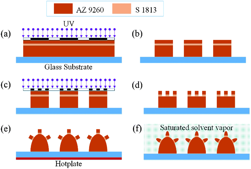
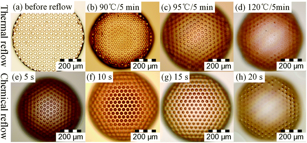
Fig. 1 shows the process flow of the hierarchic reflow method. It starts with a spin coating process so that a tri-layer photoresist film was deposited on a glass substrate. Here two common positive photoresists AZ9260 (AZ electronic materials) and S1813 (Shipley1813, Shipley) are applied as the bottom/top layer and interlayer, respectively. This is to take advantage of their distinct difference in the glass transition temperatures (Tg), which makes it possible to fabricate the curved substrate and ommatidia of the BCEs step by step via different reflow processes. Next, the photolithography process is employed to pattern the tri-layer film. By tuning the exposure dosage and developing time, the photoresist film was patterned in two steps and to form a hierarchic type microstructure with the smaller-diameter cylinder array sitting on the top of the larger-diameter cylinder array as shown in Fig. 1(a)–(d). After that, the sample was placed on a hotplate to conduct the thermal reflow process to fabricate the microlens substrate as shown in Fig. 1(e). Basically, the annealing temperature for the thermal reflow process should be set in between the Tg values of AZ9260 (around 90 °C) and that of S1813 (around 170 °C). With such a temperature setting, the bottom AZ9260 cylinder melts to form a microlens with a spherical surface, which is used as the curved substrate of the BCE array. However, the S1813 interlayer and the upper AZ9260 cylinders resting on it still maintain their original shapes without changing. This can be explained from two aspects. On the one hand, the S1813 photoresist acts as an interfacial layer to prevent the diffusion between the top and bottom AZ9260 photoresists. In this way, is not possible for the top AZ9260 photoresist to merge with the bottom one through the diffusion process during the annealing at elevated temperature. On the other hand, since the temperature gradient exists from the hotplate surface to air, the real temperature applied on the bottom AZ9260 cylinders is in fact higher than that applied on the upper AZ9260 cylinders. If the annealing temperature can be controlled carefully so that the temperature applied on the upper cylinders is lower than the glass transition temperature, it will not melt and can still retain its original shape. It was found that this can be realized by setting the annealing temperature just marginally exceeding the Tg of AZ9260. In this case, the bottom cylinders will reflow to form a spherical surface without changing the shape of the upper cylinders. However, if the annealing temperature cannot be controlled precisely, the bottom cylinder cannot be reflowed sufficiently to form a spherical surface as shown in Fig. 2(b) or the upper cylinders will merge into the bottom larger cylinders as shown in Fig. 2(d). It should be noted here that the precise control on the annealing temperature makes it impossible to achieve the BCE structure by only employing the thermal reflow process. In order to fabricate the ommatidia on the curved surface, the other reflow method, i.e. the chemical reflow method, needs to be adopted as well. As shown in Fig. 1(f), the sample after the thermal reflow process was then put into a saturated solvent vapour atmosphere. In this case, the upper cylinder absorbs solvent and becomes less viscous so that it melts and forms a microlens shape. Since the solvent can be absorbed by both bottom and upper cylinders, therefore, the annealing time for this process should be controlled carefully and precisely again to prevent the fusion and merging of the upper cylinder into the bottom one. As demonstrated in Fig. 2(e)–(g), the shape of the obtained ommatidia can be well maintained with the annealing time of no more than 15 seconds. Whereas overlong annealing time (20 s) is detrimental because the ommatidia and the curved substrate start to merge as shown in Fig. 2(h). After the chemical reflow process, the formed BCE was placed in air for 5 minutes for the final solidification. It is worth pointing out that the whole fabrication process lasts for only around one hour.
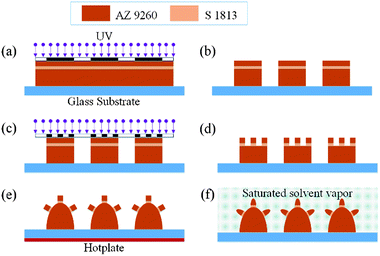 |
| | Fig. 1 Schematic illustration of the process flow of the hierarchic reflow method: (a)–(d) fabrication of a hierarchic cylinder-on-cylinder photoresist pattern array by employing the photolithography process twice, (e) fabrication of the curved substrate of the micro-BCE by means of thermal reflow and (f) fabrication of the ommatidia of the micro-BCEs via chemical reflow. | |
 |
| | Fig. 2 Photographs of the photoresist pattern before and after reflow with various reflowing parameters: (a) the original hierarchic cylinder-on-cylinder pattern before thermal reflow, (b)–(d) thermal reflow at different temperatures, and (e)–(h) chemical reflow at different times. | |
3. Results and discussion
3.1 Geometrical tests
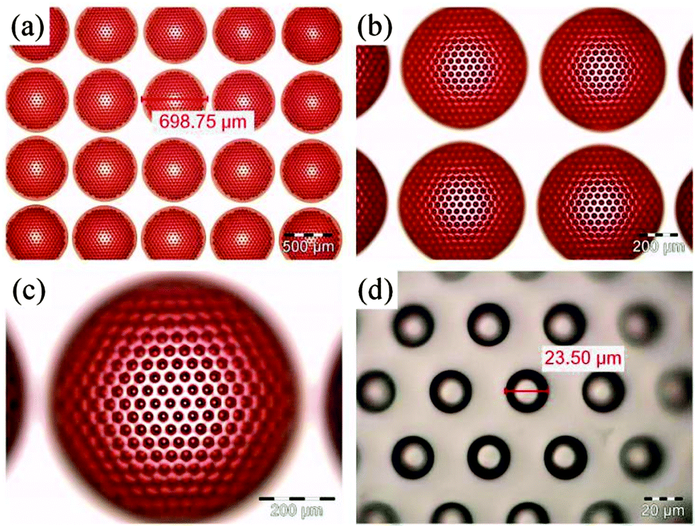
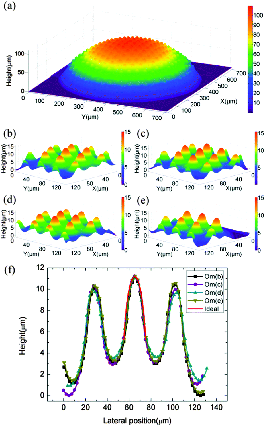
Fig. 3 shows the photographs of the fabricated micro-BCE array obtained by using an optical microscope (MX61-F, Olympus). As is shown, the size of each BCE has a diameter of around 698 μm, which is rather close to the designed value of 700 μm. Further measurements show that the error of the BCE diameter is less than 10 μm (2%) and the standard deviation is only 2.48 μm, which shows a good uniformity of the BCE array. Fig. 3(d) shows the close-up view of the ommatidia. The measured average diameter of ommatidia is around 23 μm with a standard deviation of 1.19 μm. In comparison with the designed value of 25 μm, again it has a good uniformity of around 92%. To investigate the 3D profile of the micro-BCE, a scanning laser confocal microscope (OLS4000, Olympus) was used and the measurement results are shown in Fig. 4. As can be seen from Fig. 4(a), the ommatidia align orderly on the surface of the bottom microlens whose diameter and sag height are around 700 μm and 102 μm, respectively. Furthermore, the surface profiles of the ommatidia in both the central and outer regions of the BCE were obtained and are shown in Fig. 4(b)–(e). Fig. 4(f) shows a comparison of the cross-sectional profiles of the fabricated ommatidia with those of an ideal spherical shape. As shown, the profiles of the central ommatidia match well with those of the ideal one. However, little discrepancy shows up in side ommatidia, which is caused by the undesired rotation or tilt of the BCE substrate during the test. Overall, the geometrical characterizing results indicate a good uniformity of the fabricated BCE array.
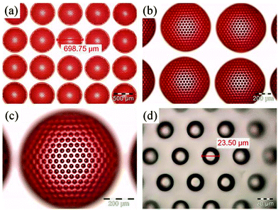 |
| | Fig. 3 Top view of the fabricated BCE array with different scales: (a), (b) the BCE array, (c) a single BCE in the array, and (d) a close-up picture of the ommatidia. | |
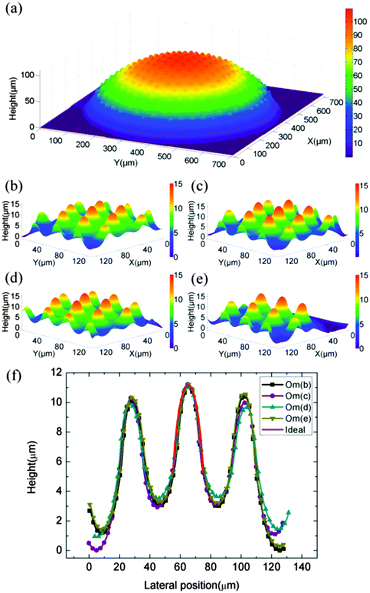 |
| | Fig. 4 Confocal microscopic characterization results of the obtained micro-BCE: (a) overall morphology, (b)–(e) zoom-in pictures of ommatidia at different positions of the BCE (from center to rim, sequentially), and (f) cross-sectional profiles of the ommatidia (“Ideal” represents an ideal spherical shape and “Om(b)”–“Om(e)” correspond, respectively, to the ommatidia shown in (b)–(e)). | |
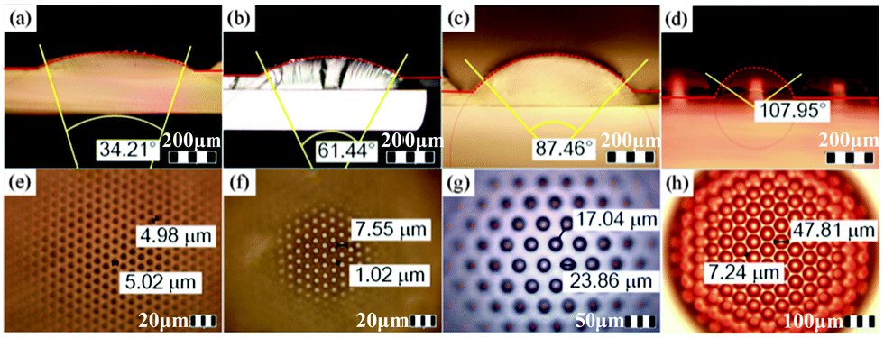
In fact, the method proposed here is quite flexible so that the geometries of both the curved base and ommatidia of the BCE can be tailored separately by controlling the geometries of the original hierarchic cylindrical structure, i.e. its diameter and thickness. To prove this point, BCEs with various shapes were also fabricated. As shown in Fig. 5(a)–(d), BCEs with FOVs ranging from 34.21° to 107.95° have been obtained successfully. Fig. 5(e)–(h) show the formed ommatidia with a diameter ranging from 5.02 μm to 47.81 μm and a filling factor ranging from about 40.5% to 79.6%. It is found that the numerical aperture (NA) of the ommatidia ranging from 0.09 to 0.45 can be obtained, which is a quite large scope and shows the great flexibility of this method. It should be noted that the fabricated BCE in photoresists can be transferred into the more transparent polymer, i.e. UV-curable epoxy resin (NOA68, Norland Products Inc. Cranbury, N.J.) by soft-lithography to improve the transparency and the imaging properties of the BCE further.12 In fact, the fabricated micro-BCE array in photoresists was replicated into the transparent NOA68 by the soft-lithographic method. The replicated NOA micro-BCE array was then used to characterize its imaging performance in the following section.
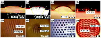 |
| | Fig. 5 Photographs of fabricated BCEs with different FOVs and ommatidia geometries: (a)–(c) cross-sectional images of BCEs with a base diameter of 700 μm, (d) side view of a BCE with a base diameter of 300 μm, and (e)–(h) photographs of BCEs with different ommatidium sizes and fill factors. | |
3.2 Optical tests
To characterize the optical performance of a particular BCE array (corresponding to Fig. 5(c) and (g)), the point spread function (PSF) was tested using a home-built setup depicted in Fig. 6(a). As shown in Fig. 6(a), the mirror was moved and tilted with different angles to ensure that the laser beam incidents perpendicularly onto different positions (from center to edge) of the BCE. Airy patterns of the ommatidia were captured using a high magnification microscope. Fig. 6(b) shows the lateral intensity distribution of 2D PSFs with different incident angles along the y-axis. As shown in Fig. 6(b), the measured PSFs match quite well with the ideal one even for the case with an incident angle as large as 40°, which indicates a good uniformity of the optical performance of the fabricated BCE at a large FOV of around 80°. According to classical diffraction theory, the NA of the ommatidium was calculated to be 0.45.
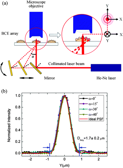 |
| | Fig. 6 PSF test of the fabricated micro-BCE array: (a) configuration of the test setup and (b) 2D PSFs of the ommatidia. | |
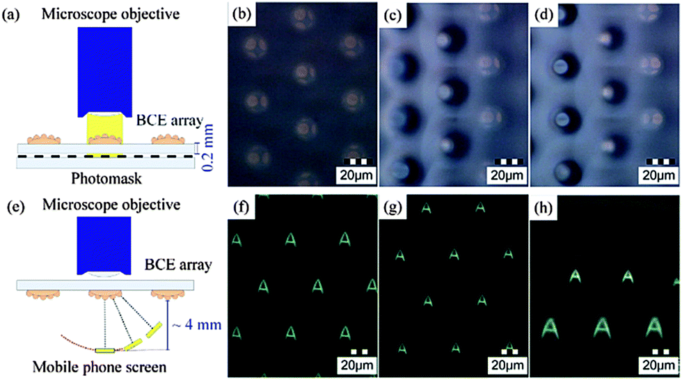
To further characterize its optical performance, replicated NOA micro-BCE array was used to image various objects. Firstly, a binary glass/chromium photomask was adopted as the object to test the resolving power of the BCE as shown in Fig. 7(a). The pattern on the photomask is the circle array with a diameter of 100 μm and a spacing of 20 μm. In this case, the BCE array was placed directly on the surface of a photomask and then a microscope was focused on different positions of the BCE to capture images formed by the ommatidia. As shown in Fig. 7(b)–(d), the obtained images are quite clear so that even the narrow spacing between the circles can be resolved clearly. Besides, a setup depicted in Fig. 7(e) was used to test the wide FOV imaging performance of the BCE. As illustrated, the BCE was put upside down with its ommatidia facing the object (bright letter “A” with a width of around 1.7 mm displayed by a mobile phone). To mimic a curved object plane for the BCE, the target is placed at multiple positions roughly on an arc which has a common center, i.e. the BCE. Fig. 7(f)–(h) show the images formed by ommatidia in different regions of the BCE. As can be seen, the obtained images are quite clear with sharp edges in Fig. 7(f) and (g). However, the distortion of the images in Fig. 7(h) can be clearly seen. The distortion of the image is caused by the combining effect of the defocus and off-axis aberrations of the objective of the microscope, which suggests that an imaging detector with a curved surface should be used to capture the aberration free image formed by the BCE. In general, the optical testing results indicate that the fabricated BCE has a fair imaging property.
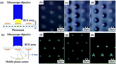 |
| | Fig. 7 Imaging test setups for the micro-BCE array to form minified real images with different objects: (a) a photomask and (e) a mobile phone screen. (b)–(d) and (f)–(h) are obtained images of the photomask and the mobile phone screen, which are formed by the ommatidia located at the center, middle and the edge of the BCE, respectively. | |
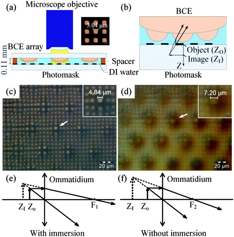
Besides the above optical tests, the fabricated BCEs were also used to form a magnified virtual image of patterns on a photomask. The photomask has a pattern of square arrays with each square having a side length of 3 μm. Fig. 8(a) depicts the schematic of the imaging setup in which the BCE array is put upside down with the ommatidia facing the photomask. DI water was filled in the chamber formed by the BCE array and the photomask. That is to say, the BCE is in fact immersed in DI water. The BCE used here has a sag height of 102 μm for its curved base and a focal length of 28 μm (in air) for its ommatidia (corresponding to the BCE shown in Fig. 3 and 4). To control the objective distance, spacers with a thickness of 110 μm were applied in between the BCE array substrate and the photomask surface. In this case, a virtual image of the object has been formed by the ommatidia in the central region of the BCE, which is shown in Fig. 8(b). Here, a 100× microscope objective was used to capture the magnified virtual images formed by the ommatidia. Fig. 8(c) and (d) show the final images captured with the test configuration described above with and without water immersion during the imaging process. As can be seen from Fig. 8(c) and (d), the side length of the square images is 4.84 μm and 7.20 μm, respectively, indicating that a lower magnification is obtained in the water immersion case. This can be explained from two aspects. On the one hand, the focal length of the ommatidia is reciprocally proportional to the difference between the refractive index of the ommatidia material (NOA68 epoxy resin) and that of the surrounded material (air or water). As the refractive index of water is higher than that of air, the actual focal length of the ommatidia becomes larger in water. On the other hand, the object distance is fixed and less than one focal length of the ommatidia so that the magnification decreases as the focal length of the ommatidia increases, which is illustrated in Fig. 8(e) and (f). At the same time, it can also be seen from Fig. 8(c) and (d) that the image is clearer in the case with water immersion than the case without water immersion. This is because the difference in the refractive index is much smaller in the water immersion case so that much less amount of light is reflected from the photomask, which results in a lower background noise and hence a clearer image can be obtained.
 |
| | Fig. 8 Imaging configuration for the fabricated BCE to form a magnified virtual image: (a) schematic of the testing setup and (b) diagram of the virtual image formation by the ommatidia of the BCE. (c) and (d) are images obtained with the test configuration depicted in (a) with and without DI water immersion, respectively. (e) and (f) are diagrams of the light path for an ommatidium to form a virtual image with and without DI water immersion. | |
4. Conclusions
In conclusion, a hierarchic reflow method has been proposed and demonstrated for the monolithic fabrication of micro-BCE arrays. By this method, micro-BCE arrays with various geometries have been successfully fabricated and the characterization results indicate that a good optical performance of the BCEs can be achieved. Depending on different optical configurations, the obtained micro-BCE can form clear magnified images or minified images of the testing object, showing its prospective usage in large FOV imaging systems. Besides, the fabricated BCE array can also find potential application in LED arrays with a wide illuminating angle.
Acknowledgements
The authors acknowledge the financial support from the Natural Science Foundation of China under grant numbers 61475156, 61490712 and 61361166004. Financial support from Jilin Provincial Science and Technology Department of China under Grant no. 20140519002JH is also acknowledged. The contributions of Dr Hua Liu, Dr Hongxin Zhang and Dr Wenbin Xu to the measurement of the fabricated BCE samples are also acknowledged.
Notes and references
- G. A. Horridge, Sci. Am., 1977, 237, 108 CrossRef.
- J. Kim, K. H. Jeong and L. P. Lee, Opt. Lett., 2005, 30, 5 CrossRef PubMed.
- D. Straw, E. J. Warrant and D. C. O’Carroll, J. Exp. Biol., 2006, 209, 4339 CrossRef PubMed.
- L. P. Lee and R. Szema, Science, 2005, 310, 1148 CrossRef CAS PubMed.
- K. H. Jeong, J. Kim and L. P. Lee, Science, 2006, 312, 557 CrossRef CAS PubMed.
-
J. Duparré, D. Radtke and A. Tünnermann, in MOEMS and Miniaturized Systems VI, ed. D. L. Dickensheets, B. P. Gogoi and H. Schenk, SPIE, San Jose, United States, vol. 6466, 2007, 64660K1 Search PubMed.
- L. Li and A. Y. Yi, Opt. Express, 2010, 18, 18125 CrossRef PubMed.
- H. Zhang, L. Li, D. L. McCray, D. Yao and A. Y. Yi, Sens. Actuators, A, 2012, 179, 242 CrossRef CAS.
- Q. He, J. Liu, B. Yang, Y. Dong and C. Yang, J. Microelectromech. Syst., 2013, 22, 4 CrossRef CAS.
- Y. Cherng and G. J Su, J. Micromech. Microeng., 2014, 24, 1 CrossRef.
-
J. Xiao, Y. M. Song, Y. Xie, V. Malyarchuk, I. Jung, K. Choi, Z. Liu, H. Park, C. Lu, R. Kim, R. Li, K. B. Crozier, Y. Huang and J. A. Rogers, in Bioinspired, Biointegrated, Bioengineered Photonic Devices II, ed. L. P. Lee, J. A. Rogers and S. H. A. Yun, SPIE, San Francisco, United States, vol. 8958, 2014, p. 89580A1 Search PubMed.
- T. Wang, W. Yu, C. Li, H. Zhang, Z. Xu, Z. Lu and Q. Sun, Opt. Lett., 2012, 37, 2397 CrossRef CAS PubMed.
- B. G. Park, K. Choi, C. J. Jo and H. S. Lee, Soft Matter, 2012, 8, 1751 RSC.
- D. Wu, J. Wang, L. Niu, X. Zhang, S. Wu, Q. Chen, L. P. Lee and H. B. Sun, Adv. Opt. Mater., 2014, 2, 751 CrossRef CAS.
- S. Deng, J. Lyu, H. Sun, X. Cui, T. Wang and M. Lu, Opt. Eng., 2015, 54, 033105 CrossRef.
- R. J. Martín-Palma, A. E. Miller, D. P. Pulsifer and A. Lakhtakia, Appl. Phys. Lett., 2014, 105, 103703 CrossRef.
- K. Wei, H. Zeng and Y. Zhao, Lab Chip, 2014, 14, 3594 RSC.
- L. Wang, H. Liu, W. Jiang, R. Li, F. Li, Z. Yang, L. Yin, Y. Shi and B. Chen, J. Mater. Chem. C, 2015, 3, 5896 RSC.
- Z. D. Popovic, R. A. Sprague and G. A. Neville Connell, Appl. Opt., 1988, 27, 1281 CrossRef CAS PubMed.
- L. Erdmann and D. Efferenn, Opt. Eng., 1997, 36, 1094 CrossRef CAS.
Footnote |
| † Electronic supplementary information (ESI) available. See DOI: 10.1039/c5tc03025k |
|
| This journal is © The Royal Society of Chemistry 2016 |
Click here to see how this site uses Cookies. View our privacy policy here.