Relationship between dislocations and misfit strain relaxation in InGaAs/GaAs heterostructures
Jinping
Li
ab,
Guoqing
Miao
*a,
Yugang
Zeng
a,
Zhiwei
Zhang
a,
Dabing
Li
 a,
Hang
Song
a,
Hong
Jiang
a,
Yiren
Chen
a,
Xiaojuan
Sun
a and
Zhiming
Li
a
a,
Hang
Song
a,
Hong
Jiang
a,
Yiren
Chen
a,
Xiaojuan
Sun
a and
Zhiming
Li
a
aState Key Laboratory of Luminescence and Applications, Changchun Institute of Optics, Fine Mechanics and Physics, Chinese Academy of Sciences, Changchun 130033, P. R. China. E-mail: miaogq@ciomp.ac.cn
bUniversity of Chinese Academy of Sciences, Beijing, 100039, P. R. China
First published on 17th November 2016
Abstract
Large lattice mismatched heterostructures In0.78Ga0.22As/GaAs were grown with a low-temperature (LT) InGaAs buffer. Misfit dislocation arrays were observed at the LT-buffer/GaAs interfaces. Transmission electron microscopy (TEM) was used to investigate the microstructures of the heterointerfaces. The relationship between misfit dislocations and strain relaxation at the interface was analysed. It was found that strain redistribution gives rise to the discrepancy of interfacial structure and misfit strain relaxation for different samples. The experimental results are in favor of the conclusion and confirm the analysis we proposed.
Introduction
The ternary III–V compound InxGa1−xAs offers a wide, direct band gap, high carrier mobility and high reliability, therefore enabling wide applications in short-wave infrared photodetectors.1,2 With great demands in earth observation and spatial remote sensing, extended wavelength InxGa1−xAs (x > 0.53) photodetectors are consequently required.3,4 As InP substrates could provide a smaller lattice mismatch for InxGa1−xAs (x > 0.53) epitaxy compared with GaAs, for several applications, GaAs substrates are desirable. This is attributed to several reasons: GaAs is inexpensive compared with InP, transparent to more (long wavelength) active regions because of its wide band gap, and forms excellent n and p ohmic contacts.5 As In content increases, the lattice mismatch becomes larger and gives rise to misfit strain. The misfit dislocations induced by the strain bring detrimental effects to epilayers and devices. To maintain the expected properties of the active layer, compositionally graded metamorphic buffers have been demonstrated in InxGa1−xAs on InP and GaAs.6–9 In addition, the two-step growth technique, in which a preceding low-temperature buffer (LT-buffer) layer is deposited before a high-temperature film growth, has been confirmed to be an effective method to relieve the misfit strain in our previous study.10,11 While a mechanism about island growth has been proposed to elucidate the reduction of misfit dislocations by LT-buffer layers,6 there seems to be a need for further investigation into strain relaxation from a microscopic perspective.The relaxation of the misfit strain is of major importance for understanding the heterogeneous epitaxy.12 Misfit dislocations are responsible for the misfit strain relaxation; several theoretical and experimental studies about the dislocation formation mechanism have been carried out. Many researches were focused on 90° dislocations and 60° discolations. Otsuka et al.13 suggested that the substrate surface tilt may increase the fraction of the more efficient 90° dislocations in the GaAs/Si interface, consequently reducing the number of 60° dislocations, which are the origin of threading dislocations and stacking faults. The InxGa1−xAs/GaAs heterointerfaces have been studied by Chang et al.14 It was reported that there was a change in the dominant dislocation type from 60° at low lattice mismatch (<2%) to 90° at large lattice mismatch (>2%). The same observations were obtained in InxGa1−xAs/InP heterostructures:15 high lattice mismatches (>3%) correspond to a tangled array of 90° dislocations, and 60° dislocations dominate the interface when the lattice mismatch is less than 1%. Uchida et al.16 investigated In0.2Ga0.8As/GaAs and In0.4Ga0.6As/In0.2Ga0.8As/GaAs heterostructures by TEM, and the results showed that the confinement of dislocations near the interface differed significantly between In0.4Ga0.6As/In0.2Ga0.8As and In0.2Ga0.8As/GaAs, though the two heterostructures had the same lattice mismatch. It was inferred that the atoms in the lower layers, including the substrate, can rearrange during the growth of the upper layer, so that the relaxation of misfit strains behave in different ways. An atomic model was put forward to explain the dislocation formation mechanism in strained InxGa1−xAs/GaAs,17 and this model explained the change in the dominant type of dislocations from 60° at small lattice mismatches to 90° dislocations at large lattice mismatches.
Though significant attempts have been made, it appears that the discussions were only focused on the formation mechanism of misfit dislocations at interfaces. The investigations on the relationship between dislocations and misfit strain relaxation have never been reported. Only when we get a full understanding of the relationship can we take efficient measures to obtain excellent crystalline quality. In this study, high-resolution transmission electron microscopy (HRTEM) studies of the In0.78Ga0.22As/GaAs heterostructures with an LT-buffer are presented, and the misfit strain relaxation associated with the dislocation array is also analysed.
Experimental
In0.78Ga0.22As epilayers were grown at 650 °C with a nominal thickness of 1000 nm on In0.78Ga0.22As LT-buffer layers, which were deposited at 450 °C on (100) oriented GaAs substrates by metal-organic chemical vapor deposition (MOCVD, AIXTRON 200/4). Trimethylindium (TMIn), trimethylgallium (TMGa) and pure arsine (AsH3) were used as the In, Ga and As precursors, respectively. The base pressure of the MOCVD system was at 76 Torr. The growth rate for the In0.78Ga0.22As epilayers and LT-buffer layers were approximately 1.4 μm h−1 and 0.8 μm h−1. The V/III flux ratio for the entire growth was kept at 73. Three samples, A, B and C, with LT-buffer thicknesses of 31 nm, 85 nm and 269 nm were prepared on the premise that all the other growth conditions were kept the same.The microstructures of In0.78Ga0.22As/GaAs were characterized ex situ using transmission electron microscopy (TEM, JEM-2100F, JEOL). HRTEM was used for a [01−1] cross-section sample operating at 200 kV. The surface morphology, crystalline quality and residual strain were investigated by scanning electron microscopy (SEM, Hitachi S4800), atomic force microscopy (AFM, Hitachi S4800), high-resolution X-ray diffractometry (HRXRD, Bruker D8) and Raman spectrometry (RENISHAW InVia), respectively.
Results and discussion
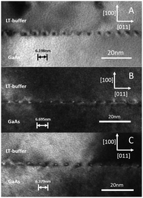
The LT-buffer thickness was determined by TEM. The full width at half maxima (FWHM) of X-ray rocking curves (RCs) from In0.78Ga0.22As epilayers were referred in ref. 6: the narrowest FWHM at 0.183° gives the best crystalline quality for sample B, compared with 0.229°, 0.270° for A and C. In addition, studies6 on the surface morphology and roughness derived the same conclusion. It is concluded that the LT-buffer layer with an appropriate thickness has an efficient misfit strain relaxation, and a thick LT-buffer may have a counter-productive effect. TEM was used to analyse the microstructure of the In0.78Ga0.22As/GaAs heterostructures.Fig. 1 shows the cross-sectional transmission electron micrograph (XTEM) images of the LT-buffer/GaAs interface along the zone axis [01−1]. All the samples present a periodic dislocation array under low magnification, as bright and dark spots, at the interfaces. It was found that the periodic dislocation array is well organized with an almost uniform spacing of 6.695 nm for sample B, whereas the other two have comparatively poor organized interfaces with an average spacing of 6.198 nm for A and 6.379 nm for C.
The HRTEM image of the LT-buffer/GaAs interface for sample A along the zone axis [01−1] is shown in Fig. 2. Each white arrow shows an extra half plane, one extra half {111} plane terminating at the (100) plane, and the edge of the two extra half planes being the characteristic of a 60° dislocation, noting the fact that complete dislocations in the diamond type structures normally have Burgers vectors of ½<110>. The Burgers vectors of the 60° dislocation here are ±½[110], ±½[101], ±½[1−10] or ±½[10−1], which are inclined from the interface by 45°.13 It is clear that 60° dislocations dominate the interface, and two faults, marked by the two-way arrow, are observed in the (1−1−1) plane and the (100) plane, respectively. The 60° dislocations distribute randomly at the interface and show a tangled arrangement. Several disordered regions are observed around the interface in Fig. 2.
Fig. 3 shows the HRTEM image of the LT-buffer/GaAs interface for sample B along the zone axis [01−1]. The edge of two extra {111} half planes is the characteristic of a 90° dislocation. The Burgers vectors of the 90° dislocations here are ±½[011] or ±½[01−1], which are parallel to the interface.13 The observed types of dislocations were all the 90° type in the selected area. These 90° dislocations are arranged in a highly periodic array with a periodicity of 6.695 nm and localized at the LT-buffer/GaAs interface. This periodicity corresponds to exactly one 90° dislocation for every 16 lattice sites of GaAs or 15 lattice sites of LT-InGaAs, which is marked in Fig. 3. No 60° dislocations or any other type of dislocations are detectable in any other locations, and disordered regions are not observed in the selected area. Considering that the best crystalline quality of epilayer is in sample B, it is concluded that the highly periodic 90° dislocation array may introduce a more effective relaxation of misfit strain than the angled 60° dislocation arrangement in sample A.
Fig. 4 is the cross-sectional HRTEM image of the LT-buffer/GaAs interface for sample C along the zone axis [01−1]. The highly periodic 90° dislocation array in Fig. 3 was not observed. Both 60° dislocations and 90° dislocations are observed at the interface. Interestingly, two 60° dislocations paired with an up-down structure are found in the image: the edge of one 60° dislocation in the pair terminates at the extra {111} plane of another 60° dislocation; it is deduced that the up-down structure may come from the glide of the 60° dislocation. It is noted that there are two extra half {111} planes separated by about 1 nm, as shown in Fig. 4. A similar phenomenon was observed in ref. 18; the authors suggested that the extra half planes with a separation of up to 2 nm compose an ‘imperfect’ 90° dislocation. Therefore, the pair of the extra half {111} planes here were identified as an ‘imperfect’ 90° dislocation. Moreover, another two extra half {111} planes marked by a red circuit are observed at the interface; one plane is terminated at the other plane.
Our experimental results indicate that the dislocation distribution at the interface influences the crystalline quality of In0.78Ga0.22As epilayers; in other words, there is a strong correlation between the dislocation arrays and misfit strain relaxation. Therefore, based on the experimental results shown above, we will try to analyse and understand the misfit strain relaxation from a microscopic point of view.
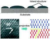
Because of a large lattice mismatch (5.6%) the LT-buffer layer shows an island growth.6 Atoms were deposited gradually on the GaAs surface to form islands. The InGaAs LT-buffer has a larger lattice constant than GaAs and therefore, the atoms will occupy the pseudomorphic position of epitaxial crystals, thereby creating strained bonds. When more bonds are formed during the deposition, it may become energetically unfavorable for next atom to occupy the normal position due to the accumulated strain. The atom may choose a low energy position with less strain, which does not correspond to the crystalline structure so that the misfit strain is relaxed. The 60° dislocations will be generated in this way and they will be located on isolated islands, which are free of any coalescence.19Fig. 5 shows the projection of the atomic arrangement of a 60° dislocation. When the LT-buffer was thin, the growth surface would be covered with isolated islands. The strain distribution in each island would differ a lot and therefore, the distribution of 60° dislocations will be different from each other and show an irregular arrangement. Furthermore, slight influences from growth condition, such as temperature maintenance, and flux fluctuation, may serve as another reason for the tangled arrangement of 60° dislocations at the interface. It is less strained among the islands due to the absence of coalescence; the 60° dislocations on the islands will occupy stable positions with low energy; this will lead to a relatively low residual strain in the LT-buffer, and hence a low strain will be propagated to the upper layer; a residual strain of −8.48 × 10¹⁰ dyn cm−1 in the In0.78Ga0.22As epilayer confirms the inference.
 | ||
| Fig. 5 The schematic of island growth when the LT buffer was thin; the projection of atomic arrangement of a 60° dislocation. | ||
As the islands' size increases, numerous coalescences occur between the islands to form an integrated layer. The LT-buffer layers are of a uniform distribution of strain. The process can be explained as follows: several islands coalesce to form a nominally large island, which can be seen as an independent unit. The strain in the former isolated islands is disturbed and redistributed with a new stable state in the independent unit. Then, as the large islands continually coalesce to form larger units, the strain distribution occurs again.
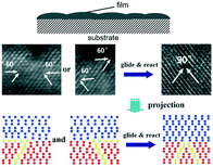
This process is repeated during the LT-buffer growth eventually forming a layer with a uniformly distributed strain. In the process of strain redistribution, the atomic bonds will be rearranged to adapt to the new configuration, and the 60° dislocations are driven to glide in the planes. It is suggested17 that a 90° dislocation can be formed by the interaction of two 60° dislocations: ½[101] + ½[1−10] = ½[011] or ½[101] + ½[110] = ½[01−1]. Herein, it is believed that the 90° dislocations at the interface originate from the interactions of 60° dislocations present in sample A. Just like Fig. 6 shows, every two 60° dislocations with different Burgers vectors glide in the planes and react to form 90° dislocations. The continuous strain distribution promotes 60° dislocations to glide and react. A large amount of 90° dislocations are produced in this way at the interface. Because the LT-buffer layer now can be regarded as a complete part or unit, there are a few discrepancies of strain distribution in the layer; in other words, the strain distribution in the entire layer tends to submit to a uniform and stable state. This uniform strain distribution gives rise to a uniform arrangement of 90° dislocations. As a result, these 90° dislocations at the interface are shown as a highly periodic array with an almost uniform spacing.
 | ||
| Fig. 6 Schematic of the LT-buffer when numerous islands coalesce; the projection of atomic arrangement of 90° dislocation, which was a result of the reaction from the two 60° dislocations. | ||
As Rocher et al. reported,20 the 90° dislocation has a 100% efficiency in the relaxation of misfit strain, compared to only 25% for a 60° dislocation. The smaller dislocation spacing in sample A can be expected to attribute to the inefficiency of the 60° dislocations for strain relaxation compared to the 90° type. The large misfit strain due to the lattice mismatch should be largely relaxed by the highly periodic 90° dislocation array in sample B. In the following, the strain energy density, Eε, and the energy density dissipated from the 90° dislocation array, E′d, are calculated and compared to evaluate the relaxation of misfit strain.21 The strain energy density is found using Eε = ε2Bh, where ε = as − af/af and B = 2μf(1 + υ)/(1 − υ). In these equations, ε is the in-plane strain, B is a constant, h = 1.878 nm is the thickness of the strained material measured by TEM, as = 0.56536 nm and af = 0.59698 nm are the lattice constants of the GaAs substrate and the relaxed LT-InGaAs layer, υ = 0.31 is the GaAs Poisson's ratio, and μf = 2.1668 × 10¹⁰ N m−2 is the In0.78Ga0.22As shear modulus, which is obtained from the formula22μf = 0.369 − 0.214 + 0.024x2, where x is the In content of the LT-buffer. The dislocation energy per unit area dissipated by the 90° dislocation array is calculated by E′d = Ed/S, where Ed ≈ μfb2/4π(1 − ν)6 is the energy per unit length of a single 90° dislocation,  is the Burgers vector along the [011] direction, and S = 6.1938 nm is the 90° dislocation spacing measured from the TEM images. A comparison of values between Eε = 0.43370 J m−2 and E′d = 0.45967 J m−2 for a strained film thickness of 1.878 nm indicates that the 90° dislocation array relieves about 94.35% of the strain energy generated by the lattice mismatch, an almost full strain relaxation at the interface. The residual strain6 in the epilayer is −7.79 × 10¹⁰ dyn cm−2, the lowest among all the samples; this reflects the low strain propagated from the LT-buffer. Therefore, it is concluded that the interface of the highly periodic 90° dislocation array gives a great relaxation of the misfit strain and leads to the superior crystalline quality of the epilayer.
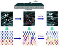
When growth continues, the strain in the LT-buffer is expected to increase as the islands grow due to the accumulation of misfit strain.19 In addition, the energy induced by the thermal strain will rise as the thickness increases.6,23 It is considered that the misfit strain relaxation of 90° dislocations in sample B may reach a saturation point, so that no more extra misfit strain could be relaxed by the dislocation array. When the LT-buffer becomes thicker, the periodic dislocation array at the interface cannot be maintained due to the increasing strain, and it tends to break down. As a previous report suggested,16 the atoms in the lower layers, including the substrate, can rearrange during the growth of the upper layer. The atomic bonds will be rearranged and the strain will be redistributed. The interface as well as the LT-buffer structure become increasingly complex. Although 90° dislocations are generally recognized sessile, and unlikely to glide in the planes, we believe that the 90° dislocations would be split into 60° dislocation pairs under great strain. As Fig. 7 shows, when the 90° dislocation is under strain along the [1−1−1] or [111] direction, as the arrows point towards, it divides into two 60° dislocations. Therefore, it is supposed that the 60° dislocations pair in Fig. 4; one is below the other, resulting from the decomposition of 90° dislocations. The pair of extra half {111} planes marked by a red circuit in Fig. 4 is now explained to be a result of a 90° dislocation that was on the verge of decomposition under the great strain. The decomposition of 90° dislocations, from one aspect, also indicates the presence of great strain in the LT-buffer layer due to the increasing thickness. As a result, the misfit strain relaxation at the interface is far less effective than the highly periodic 90° dislocation array because the relaxation efficiency of 90° dislocations is four times that of the 60° types.20 Although other dislocations could be generated in the LT-buffer to relax the extra strain, they are far less effective than the 90° dislocation array. The relaxation of the misfit strain did not keep pace with the increasing strain, resulting in a large residual strain in the LT-buffer which could be propagated to the epilayer. The residual strain of −1.30 × 10¹¹ dyn cm−2 in the epilayer has proven this to some extent.
 | ||
| Fig. 7 When the LT-buffer becomes thicker, the 90° dislocation is split into two 60° dislocations under a greater strain. The projection of atomic arrangement of the decomposition is shown. | ||
Conclusion
In summary, the LT-buffer layer inserted in the In0.78Ga0.22As/GaAs is effective at relaxing the strain due to the lattice mismatch. The experimental results showed that for different samples, different types of dislocations dominate the heterointerfaces, and the highly periodic 90° dislocation array leads to the most effective relaxation of misfit strain and a superior crystalline quality of the epilayer. The relationship between dislocations and strain relaxation was analysed. It is believed that the strain distribution could cause rearrangement of atoms during the LT-buffer growth; this process promotes the generation and interaction of the dislocations at the interfaces, leading to different states of strain relaxation. Experimental results and analysis support the conclusions we proposed. Work is in progress to obtain better knowledge of misfit strain relaxation. It is anticipated that we would be capable of taking efficient measures to manipulate the dislocations and strain to obtain superior crystalline quality and the excellent device performance.Acknowledgements
This study was supported by the National Key Research Program of China (No. 2016YFB0402401), and the Jilin Provincial Science and Technology Department (No. 20140520117JH).Notes and references
- G. Miao, T. Zhang, Z. Zhang and Y. Jin, CrystEngComm, 2013, 15, 8461–8464 RSC.
- Y. Arslan, F. Oguz and C. Besikci, Infrared Phys. Technol., 2015, 70, 134–137 CAS.
- A. M. Joshi, V. S. Ban, S. Mason, M. Kazakia and W. F. Kosonocky, 512-and 1024-element linear InGaAs detector arrays for near-infrared (1-3μm) environmental sensing. San Diego'92. International Society for Optics and Photonics, December, 1992 Search PubMed.
- V. S. Ban, G. Erickson, S. Mason, K. Woodruff, G. Gasparian and G. H. Olsen, Room-Temperature Detectors For 800-2600nm Based On InGaAsP Alloys. 1989 Orlando Symposium. International Society for Optics and Photonics, September, 1989 Search PubMed.
- A. Jallipalli, G. Balakrishnan, S. Huang, T. Rotter, K. Nunna, B. Liang, L. Dawson and D. Huffaker, Nanoscale Res. Lett., 2009, 4, 1458–1462 CrossRef CAS PubMed.
- J. Li, G. Miao, Z. Zhang and Y. Zeng, CrystEngComm, 2015, 17, 5808–5813 RSC.
- A. Gocalinska, M. Manganaro and E. Pelucchi, Appl. Phys. Lett., 2012, 100, 152112 CrossRef.
- M. di Forte-Poisson, C. Brylinski, J. Di Persio, X. Hugon, B. Vilotitch and C. Le Noble, J. Cryst. Growth, 1992, 124, 782–791 CrossRef CAS.
- T. Zhang, G. Miao, Y. Jin, S. Yu, H. Jiang, Z. Li and H. Song, Mater. Sci. Semicond. Process., 2009, 12, 156–160 CrossRef CAS.
- T. Zhang, G. Miao, Y. Jin, H. Jiang, Z. Li and H. Song, J. Alloys Compd., 2008, 458, 363–365 CrossRef CAS.
- T. Zhang, G. Miao, Y. Jin, S. Yu, H. Jiang, Z. Li and H. Song, J. Alloys Compd., 2009, 472, 587–590 CrossRef CAS.
- A. Rocher and E. Snoeck, Thin Solid Films, 1998, 319, 172–176 CrossRef CAS.
- N. Otsuka, C. Choi, Y. Nakamura, S. Nagakura, R. Fischer, C. Peng and H. Morkoc, Appl. Phys. Lett., 1986, 49, 277–279 CrossRef CAS.
- K. H. Chang, P. K. Bhattacharya and R. Gibala, J. Appl. Phys., 1989, 66, 2993–2998 CrossRef CAS.
- M. Gendry, V. Drouot, C. Santinelli, G. Hollinger, C. Miossi and M. Pitaval, J. Vac. Sci. Technol., B: Microelectron. Nanometer Struct.--Process., Meas., Phenom., 1992, 10, 1829–1834 CrossRef CAS.
- Y. Uchida, H. Kakibayashi and S. Goto, J. Appl. Phys., 1993, 74, 6720–6725 CrossRef CAS.
- Y. Chen, X. Lin, Z. Liliental-Weber, J. Washburn, J. Klem and J. Tsao, Appl. Phys. Lett., 1996, 68, 111–113 CrossRef CAS.
- N. Jin-Phillipp, W. Sigle, A. Black, D. Babic, J. Bowers, E. Hu and M. Rühle, J. Appl. Phys., 2001, 89, 1017–1024 CrossRef CAS.
- W. Qian, M. Skowronski, R. Kaspi, M. De Graef and V. Dravid, J. Appl. Phys., 1997, 81, 7268–7272 CrossRef CAS.
- A. Rocher and E. Snoeck, Mater. Sci. Eng., B, 1999, 67, 62–69 CrossRef.
- S. Huang, G. Balakrishnan, A. Khoshakhlagh, A. Jallipalli, L. Dawson and D. Huffaker, Appl. Phys. Lett., 2006, 88, 131911 CrossRef.
- H. Detz and G. Strasser, Semicond. Sci. Technol., 2013, 28, 085011 CrossRef.
- Y. Takano, M. Hisaka, N. Fujii, K. Suzuki, K. Kuwahara and S. Fuke, Appl. Phys. Lett., 1998, 73, 2917–2919 CrossRef CAS.
| This journal is © The Royal Society of Chemistry 2017 |


